
 Open Access Article
 This Open Access Article is licensed under a Creative Commons Attribution-Non Commercial 3.0 Unported Licence
Enhanced efficiency and high temperature stability of hybrid quantum dot light-emitting diodes using molybdenum oxide doped hole transport layer†
Jinyoung Yuna,
Jaeyun Kimb,
Byung Jun Jungc,
Gyutae Kim *a and
Jeonghun Kwak*d
*a and
Jeonghun Kwak*d
aSchool of Electrical Engineering, Korea University, Seoul 02841, South Korea. E-mail: gtkim@korea.ac.kr
bSchool of Electrical and Computer Engineering, University of Seoul, Seoul 02504, South Korea
cDepartment of Materials Science and Engineering, University of Seoul, Seoul 02504, South Korea
dDepartment of Electrical and Computer Engineering, Inter-University Semiconductor Research Center, Seoul National University, Seoul 08826, South Korea. E-mail: jkwak@snu.ac.kr
First published on 24th May 2019
Abstract
High power efficiency (PE) and stability of quantum dot (QD) light-emitting diodes (QLEDs) are important factors for practical use in various displays. However, hybrid QLEDs consisting of an organic hole transport layer (HTL) and an inorganic electron transport layer (ETL) sometimes have poor stability due to the low thermal stability of the organic HTL. To solve the problem, here, we report enhanced efficiency, lifetime, and temperature stability in inverted and hybrid structured QLEDs by adopting a MoO3-doped HTL. Also, to improve the electron–hole charge carrier balance, a thin insulating interlayer was used between QDs and the ETL. As a result, the QLED with the p-doped HTL exhibited the increased PE by ∼28% and longer lifetime compared to the pristine QLEDs. In addition, the QLED showed stable operation at the high temperature up to 400 K, whereas the control device failed to operate at 375 K. We systematically investigated the effect of the MoO3-doping on the performance and thermal stability of the QLEDs. We believe that QLEDs with the p-doped HTL can be used for further QLED researches to simultaneously improve the efficiency, lifetime, and high temperature stability, which are highly required for their use in automotive and outdoor displays.
1. Introduction
Colloidal nanocrystal quantum dots (QDs) exhibit several unique characteristics as an emitter, such as high photoluminescence (PL) quantum yields (QYs), size-controlled tunability of emission wavelengths, and narrow emission spectra based on a strong quantum confinement effect.1–6 Due to the outstanding optical properties, QDs attract attention for full colour display devices with a wide colour gamut (WCG) and high power efficiency. In particular, since the first QD-based light-emitting diodes (QLEDs) were introduced about two decades ago,7 their performance has been rapidly improved though multidisciplinary, extensive researches and developments on QDs, ligands, and device structures. In particular, the maximum efficiency of Cd-based QLEDs are comparable with that of phosphorescent organic light-emitting diodes (OLEDs),8,47 which made QLEDs be one of the most promising candidates for the next-generation display devices. However, the QLEDs still need to be ameliorated in terms of the efficiency, lifetime, and temperature stability to cope with the expansion of display industry toward non-consumer electronic devices, such as automotive displays and public displays.A plenty of QLED researches have been conducted based on organic–inorganic hybrid device structures consisting of n-type metal oxides (e.g., ZnO, SnO2 or TiO2) as an electron transport layer (ETL) and p-type small molecules or polymers as a hole transport layer (HTL).9–15 This structure has several advantages, such as energy level alignment for facilitated electron/hole charge carrier injection into QDs and easy processability for the multi-layered stacking. As a result, hybrid QLEDs exhibit much higher performance in terms of efficiency, turn-on voltage (Von), and lifetime, compared to the devices using all-organic6,16,17 or all-inorganic18 transport layers.
On the other hand, the hybrid device structure has a few demerits to be solved. The most typical issue is electron–hole carrier imbalance during operation. Several phenomena, such as hole leakage current at the imperfect interface between QDs and the metal oxide ETL,19 negative charging of QDs by excessive electrons in the metal oxide ETL,20 and the intrinsic difference of the charge carrier density and mobility between inorganic ETLs and organic HTLs,21 are related to the electron–hole imbalance. Thus, reduced efficiency, poor operational stability, and severe efficiency roll-off can be observed mostly in hybrid QLEDs.22–25 Recently, a few strategies have been introduced to improve the charge balance. Among the methods, inserting a thin interlayer between the QD emission layer (EML) and the metal oxide ETL is a widely used and effective strategy to control excess electron injection into QDs. For instance, a thin layer of insulating polymers, such as polymethyl methacrylate (PMMA),26,27 polyethylenimine ethoxylated (PEIE),28,29 polyethylenimine (PEI),30 and poly(4-vinylpyridine) (PVPy)31 was adopted at the EML/ETL interface. These insulating polymers efficiently suppress excess electron injection into QDs, exciton–polaron quenching and hole leakage current at the interface, leading to the improvement of the external quantum efficiency (EQE), current efficiency (CE), and operational stability of the QLEDs. However, reduced electron current by the insulating layer inevitably brings about high driving voltages and reduced power efficiency (PE),26,27,31 which deteriorates the merits of using an interlayer in QLEDs.
In this letter, we introduce a novel hybrid QLED structure exhibiting good electron–hole balance, mainly originating from (i) enhanced hole current by adopting a molybdenum trioxide (MoO3) doped HTL (p-doping) and (ii) suppressed excess electron injection and hole leakage current by using a PVPy interlayer. These devices thereby could show high PE, low driving voltages, and enhanced lifetime. In addition, the incorporation of the MoO3 doped HTL enabled stable operation of the QLEDs at a high temperature condition of ∼400 K, which is a primary requisite factor for automotive and outdoor applications.
2. Experimental method
Pre-patterned indium-tin-oxide (ITO) glass substrates were cleaned in an ultrasonic bath with acetone and de-ionized water and then dried in an oven at 120 °C. Green-emitting core/shell QDs in a chemical composition of CdZnSeS/ZnS were purchased from Invisible, Inc. The UV-Vis absorption and PL spectra are displayed in Fig. S1(a) in ESI.† ZnO nanoparticles (NPs) were synthesized according to the previously reported synthetic procedures32 and dispersed in butanol. Poly(4-vinylpyridine) (PVPy, weight average molecular weight ∼60![[thin space (1/6-em)]](https://www.rsc.org/images/entities/char_2009.gif) 000) and MoO3 were purchased from Sigma-Aldrich, and 4,4′-bis(N-carbazolyl)-1,1′-biphenyl (CBP) was purchased from Lumtec. All the commercial materials were used as received. The dispersion solution of ZnO NPs with a concentration of 30 mg mL−1 was spin-coated at 2000 rpm for 60 s as the ETL and thermally annealed on a hot plate at 90 °C for 30 min. PVPy dissolved in methanol with a concentration of 0.5 mg mL−1 and QDs dispersed in hexane with a concentration of 10 mg mL−1 were sequentially spin-coated at 4000 rpm for 30 s on the top of the ZnO layer, and then dried at 75 °C for 10 min, respectively. After drying, CBP, MoO3, and Al as the HTL, HIL, and anode, respectively, were thermally evaporated under a high vacuum pressure of <3 × 10⁻⁷ torr. For the metal oxide-doped HTL, CBP and MoO3 were co-deposited in the same chamber. The QLED device structure and the energy band diagrams are depicted in Fig. 1(a) and (b), respectively.
000) and MoO3 were purchased from Sigma-Aldrich, and 4,4′-bis(N-carbazolyl)-1,1′-biphenyl (CBP) was purchased from Lumtec. All the commercial materials were used as received. The dispersion solution of ZnO NPs with a concentration of 30 mg mL−1 was spin-coated at 2000 rpm for 60 s as the ETL and thermally annealed on a hot plate at 90 °C for 30 min. PVPy dissolved in methanol with a concentration of 0.5 mg mL−1 and QDs dispersed in hexane with a concentration of 10 mg mL−1 were sequentially spin-coated at 4000 rpm for 30 s on the top of the ZnO layer, and then dried at 75 °C for 10 min, respectively. After drying, CBP, MoO3, and Al as the HTL, HIL, and anode, respectively, were thermally evaporated under a high vacuum pressure of <3 × 10⁻⁷ torr. For the metal oxide-doped HTL, CBP and MoO3 were co-deposited in the same chamber. The QLED device structure and the energy band diagrams are depicted in Fig. 1(a) and (b), respectively.
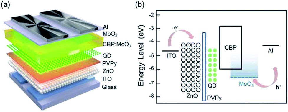 | ||
| Fig. 1 (a) Inverted QLED device structure and (b) its energy band diagram. | ||
The current density (J)–voltage (V)–luminance (L) properties and the electroluminescence (EL) spectra were measured using a Keithley 2400 source measure unit and a Konica Minolta CS-2000 spectroradiometer. The temperature dependent J–V characteristics were obtained using a liquid nitrogen cooled cryostat system while the temperature was controlled using a proportional-integral-derivative (PID) temperature controller (LakeShore Model 335 Cryogenic Temperature Controller) which monitors the sample temperature using two silicon diode sensors. The absorption spectra were characterized using a UV-Vis spectrophotometer (Shimadzu UV3105PC). The surface morphology was obtained using an atomic force microscope (AFM, Park Systems NX10) in a non-contact mode. The operating temperature distribution and infrared (IR) images of the QLEDs were measured using an IR camera (FLIR A325sc). The capacitance (C)–V and resistance (R)–V curves were measured using an LCR meter (Hewlett Packard 4284A) with an oscillation amplitude of 25 mV and a frequency of 10 kHz.
3. Results and discussion
Among several transition metal oxides (TMOs), MoO3 was chosen as the p-type dopant in this work by considering the thermal evaporation temperature and the energy levels of the host material (i.e., CBP) for higher doping efficiency.33,34 To investigate the effects of using a MoO3 doped HTL on the device performance, we fabricated green-emitting QLEDs with four different structures as follows:Device A1: ITO/ZnO (40 nm)/QD (20 nm)/CBP (50 nm)/MoO3 (10 nm)/Al (80 nm)
Device A2: ITO/ZnO (40 nm)/QD (20 nm)/CBP (30 nm)/CBP:MoO3 (20 nm, 10 vol%)/MoO3 (10 nm)/Al (80 nm).
Device B1: ITO/ZnO (40 nm)/PVPy (4 nm)/QD (20 nm)/CBP (50 nm)/MoO3 (10 nm)/Al (80 nm)
Device B2: ITO/ZnO (40 nm)/PVPy (4 nm)/QD (20 nm)/CBP (30 nm)/CBP:MoO3 (20 nm, 10 vol%)/MoO3 (10 nm)/Al (80 nm).
Device A1 is a control device with a non-doped HTL (50 nm), whereas Device A2 has a HTL which consists of a p-doped HTL (20 nm) and a non-doped HTL (30 nm). In general, MoO3-doped organic thin films exhibit enhanced hole transporting properties by forming charge-transfer (CT) complexes,33 as reported in several optoelectronic devices, such as OLEDs and organic photovoltaic cells.35–40 Similarly, it is supposed that applying a p-doped HTL to QLEDs will increase the hole current through the device. Especially, it is well known that hole injection from organic HTLs into Cd-based QDs is much harder than electron injection because of the large energy barrier between the highest occupied molecular orbital (HOMO) energy level of organic HTLs and the valence band maximum (VBM) energy levels of Cd-based QDs. Therefore, it can be thought that the p-doped HTL in QLEDs will be able to enhance overall device performance.
As shown in the J–V and L–V characteristics of the devices in Fig. 2, the current density of Device A2 is much higher than Device A1. The turn-on voltage (which corresponds to the voltage for 1 cd m−2) was also decreased with the p-doped HTL by ∼0.2 V. As a result, the PE of Device A2 was higher than that of Device A1 at a low current density regime of approximately <400 mA cm−2 where the electron charge carriers are abundant. At this regime, the CE of Devices A1 and A2 was almost identical. At a higher current density regime (J > 400 mA cm−2), however, the CE and PE of Device A2 with the MoO3-doped HTL became noticeably lower than those of Device A1 without a p-doped HTL. In this case, high J is attributed to the increment of hole carriers, resulting in hole leakage current at the QD/ZnO interface and/or exciton quenching by excess hole carriers. We could thus know that the QLED performance as well as the charge balance cannot be improved for entire bias ranges by solely enhancing the hole transporting properties. The enhancement of hole transport properties of the MoO3-doped CBP film was confirmed with hole only devices (HODs) in the structure of ITO/MoO3 (10 nm)/CBP (30 nm)/CBP:MoO3 (20 nm, 10 vol%) or CBP (20 nm)/MoO3 (10 nm)/Al (80 nm). As plotted in Fig S2 in ESI,† the HOD with the p-doped HTL exhibited higher J and the conductance than that without doping.
 | ||
| Fig. 2 (a) Current density–voltage, (b) luminance–voltage, (c) current efficiency–current density and (d) power efficiency–current density characteristics of the QLEDs. | ||
To improve the charge balance with utilizing the p-doped HTL, we inserted a thin interlayer of PVPy between QDs and ZnO NPs into Device A1 and A2, designated as Devices B1 (normal HTL) and B2 (p-doped HTL), respectively. As reported previously, this non-conjugated PVPy layer can not only lower excess electron injection but also block reduce hole leakage current.31 The same results are shown in Fig. 2(a). When comparing Device A1 (without PVPy) and B1 (with PVPy), the efficiency of Device B1 at a low J regime is much higher than that of Device A1. Meanwhile, the J of both Devices B1 and B2 is lower than that of Devices A1 and A2, respectively, because of the insulating property of PVPy. Here, due to the p-doping, the J of Device B2 is higher than that of Device B1. Device B2 also exhibits higher luminance at a same voltage and lower Von of ∼3.1 V, compared to those of Device B1 with Von of ∼3.3 V, as shown in Fig. 2(b). The QLEDs with a PVPy layer exhibit a bit higher maximum luminance (Lmax) of over 210000 cd m−2, compared with the devices without a PVPy layer. The maximum CE of Devices B1 and B2 is similar as approximately 25 cd A−1, which is higher than that of the devices without PVPy, as can be seen in Fig. 2(c), originating from the improved charge balance. Moreover, it is notable that the PE of Device B2 is superior to the other QLEDs over the entire current density regions, as shown in Fig. 2(d). The maximum PE of Device B2 was 15.03 lm W−1, while those of Devices A1, A2, and B1 were 11.76, 12.20, and 12.88 lm W−1, respectively. Device B2 also endured the maximum J up to ∼1.9 A cm−2, which was the highest value among the devices. This result indicates that adopting both the MoO3-doped HTL and the PVPy interlayer is an effective method to improve the CE and PE simultaneously in hybrid QLEDs. In all the devices, the EL peak wavelength (λmax) was observed identically at 523 nm with a full width at half maximum (FWHM) bandwidth of 22 nm (Fig S1 in ESI†), meaning that MoO3-doping in the HTL have no influence on the optical properties of the QLEDs. The performance of the QLEDs is also summarized in Table 1.
| Device | Von (V) | EQE (%) | CE (cd A−1) | PE (lm W−1) | Lmax (cd m−2) | λmax (nm) | FWHM (nm) |
|---|---|---|---|---|---|---|---|
| A1 | 2.9 | 5.72 | 23.52 | 11.76 | 197000 | 523 | 22 |
| A2 | 2.7 | 4.90 | 19.82 | 12.20 | 164000 | 523 | 22 |
| B1 | 3.3 | 6.19 | 24.98 | 12.88 | 220000 | 523 | 22 |
| B2 | 3.1 | 6.24 | 25.07 | 15.03 | 216000 | 523 | 22 |
We also investigated the J–V characteristics of Devices B1 and B2 in the temperature range of 100–400 K, as shown in Fig. 3. At 100 K, Device B1 shows a trap-limited space-charge-limited-current (SCLC, J ∝ V2) shape at the bias conditions of <6 V. Then, at 150 K, a trap-filled limit (TFL, J ∝ Vα, α ˃ 2) voltage (VTFL) can be observed as ∼5 V and decreased down to ∼3.5 V as the temperature increases gradually. Meanwhile, Device B2 with a MoO3-doped HTL shows a typical temperature dependent J–V curves with the VTFL ranging from ∼4.5 V to ∼3.2 V, which were lower than those of Device B1. In other words, hole carrier concentration was increased by p-doping for all the measured temperature ranges. It is also supported by the C–V and R–V characteristics plotted in Fig. S3 in ESI.† The peak C of Device B2 (3.25 nF) was much higher than that of Device B1 (1.85 nF). The R at Von was 113 kΩ for Device B1, and it was decreased to 51 kΩ for Device B2. These results indicate that partial MoO3-doping increases hole carrier concentration and thus increases the hole transport ability of the CBP layer.
 | ||
| Fig. 3 J–V characteristics of the PVPy-inserted QLEDs with the (a) non-doped and (b) p-doped HTL, measured at 100–400 K. Device B1 failed to operate at 375 K. (c) Comparison of temperature dependent J values of two devices at 5 V. | ||
It is also noteworthy that the operating temperature of the QLEDs were highly improved by adopting a MoO3-doped HTL. Device B2 with a doped HTL showed stable operation at the temperature of up to 400 K, as shown in Fig. 3(b). Device B1 with the non-doped HTL showed overall normal operation until the temperature was increased to 350 K (Fig. 3(a)). However, severe degradation was observed at 375 K and the device was failed to operate. As mentioned above, stable operation under a high temperature condition is an essential factor for the practical use of QLEDs in automotive and outdoor displays. Fig. 3(c) compares the temperature dependent J values of two devices at 5 V.
To find out the reasons, we paid attention to the low glass transition temperature (Tg) of CBP, which is 62 °C.43 Aggregation or crystallization can be occurred in organic thin films at high temperature above Tg. We prepared two organic thin films with the same configuration of the QLEDs, which were CBP (50 nm) and CBP (30 nm)/CBP:MoO3 (20 nm, 10 vol%) films, on quartz substrates. Then, we annealed the films on a hot plate by changing the temperature from 300 K to 375 K for 30 min, and compared their UV-Vis absorption spectra. As shown in the inset photograph and curves in Fig. 4(a), the CBP-only film started to crystallize from 375 K, showing a broad absorption spectrum and white coloured aggregation of the molecules. However, the p-doped film shows no spectral and visual change while the annealing temperature changed from 300 K to 375 K, as shown in Fig. 4(b). Therefore, we can attribute the failure of Device B1 to the low Tg of the CBP HTL, and the improved temperature stability of Device B2 to the enhanced Tg of the p-doped CBP HTL, respectively. The surface morphology of the CBP and CBP/CBP:MoO3 films annealed at 375 K is compared in Fig. 4(c) and (d). The root-mean-square (RMS) roughness (Rq) of the CBP-only film was as high as ∼49 nm due to the severe aggregation/crystallization of CBP, whereas that of the MoO3-doped CBP film was ∼2 nm, at 375 K. At 300–350 K, both films exhibited the Rq of about 1–2 nm with little difference (see Fig. S4 in ESI†).
 | ||
| Fig. 4 UV-Vis absorption spectra of the (a) CBP (50 nm) and (b) CBP (30 nm)/CBP:MoO3 (20 nm, 10 vol%) films measured at various annealing temperatures of 300–375 K. Inset: photographs taken at the annealing temperature of 375 K. The surface morphology (2 μm × 2 μm) of the (c) CBP (50 nm) and (d) CBP (30 nm)/CBP:MoO3 (20 nm, 10 vol%) films measured using an AFM at 375 K. | ||
We also measured the operational lifetime of the QLEDs at the initial luminance of 1000 cd m−2, as shown in Fig. 5(a). The half lifetime was predicted by data fitting to the stretched-exponential function L(t) with the shape parameter β = 1,
| L(t) = L0exp[−(t/τ)β] |
 | ||
| Fig. 5 (a) Operational lifetime of Devices B1 and B2. Dashed lines are the predicted lifetime using the stretched-exponential function. (b) Operating temperature profile of Devices B1 and B2 through the dotted lines in the thermal images using IR camera (inset). | ||
4. Conclusions
We demonstrated enhanced performance and stability in inverted QLEDs using a MoO3-doped HTL and a PVPy interlayer. With the device structure, we could achieve increased hole injection, reduced hole leakage current, longer lifetime, and high temperature operation. The reasons for the improvement were enhanced thermal stability of the doped HTL and the improved electron–hole balance. We believe that the simple co-deposition method can be applicable for further QLED researches and the development of automotive and outdoor display devices, with improve the efficiency, lifetime, and temperature stability.Conflicts of interest
There are no conflicts to declare.Acknowledgements
This work was supported by the Industrial Technology Innovation Program (No. 10052853) funded by the Ministry of Trade, Industry & Energy (MOTIE, Korea).References
- Y. Shirasaki, G. J. Supran, M. G. Bawendi and V. Bulović, Nat. Photonics, 2013, 7, 13–23 CrossRef CAS.
- V. Wood and V. Bulović, Nano Rev., 2010, 1, 1–7 Search PubMed.
- Y. Yang, Y. Zheng, W. Cao, A. Titov, J. Hyvonen, J. R. Manders, J. Xue, P. H. Holloway and L. Qian, Nat. Photonics, 2015, 9, 259–266 CrossRef CAS.
- J. Kwak, J. Lim, M. Park, S. Lee, K. Char and C. Lee, Nano Lett., 2015, 15, 3793–3799 CrossRef CAS PubMed.
- G. J. Supran, Y. Shirasaki, K. W. Song, J. Caruge, P. T. Kazlas, S. Coe-Sullivan, T. L. Andrew, M. G. Bawendi and V. Bulović, MRS Bull., 2013, 38, 703–711 CrossRef.
- S. Coe, W. Woo, M. Bawendi and V. Bulović, Nature, 2002, 420, 800–803 CrossRef CAS PubMed.
- V. L. Colvin, M. C. Schlamp and A. P. Alivisatos, Nature, 1994, 370, 354–357 CrossRef CAS.
- H. J. Jang, J. Y. Lee, J. Kwak, D. Lee, J. Park, B. Lee and Y. Y. Noh, J. Inf. Disp., 2019, 20, 1–8 CrossRef CAS.
- T.-H. Kim, K.-S. Cho, E. K. Lee, S. J. Lee, J. Chae, J. W. Kim, D. H. Kim, J.-Y. Kwon, G. Amaratunga, S. Y. Lee, B. L. Choi, Y. Kuk, J. M. Kim and K. Kim, Nat. Photonics, 2011, 5, 176–182 CrossRef CAS.
- L. Qian, Y. Zheng, J. Xue and P. H. Holloway, Nat. Photonics, 2011, 5, 543–548 CrossRef CAS.
- J. Kwak, W. K. Bae, D. Lee, I. Park, J. Lim, M. Park, H. Cho, H. Woo, D. Y. Yoon, K. Char, S. Lee and C. Lee, Nano Lett., 2012, 12, 2362–2366 CrossRef CAS PubMed.
- Q. Sun, Y. A. Wang, L. S. Li, D. Wang, T. Zhu, J. Xu, C. Yang and Y. Li, Nat. Photonics, 2007, 1, 717–722 CrossRef CAS.
- W. Ji, Y. Lv, P. Jing, H. Zhang, J. Wang, H. Zhang and J. Zhao, ACS Appl. Mater. Interfaces, 2015, 7, 15955–15960 CrossRef CAS PubMed.
- H. Peng, W. Wang and S. Chen, IEEE Electron Device Lett., 2015, 36, 369–371 CAS.
- C. Jiang, H. Liu, B. Liu, Z. Zhong, J. Zou, J. Wang, L. Wang, J. Peng and Y. Cao, Org. Electron., 2016, 31, 82–89 CrossRef CAS.
- P. O. Anikeeva, J. E. Halpert, M. G. Bawendi and V. Bulović, Nano Lett., 2009, 9, 2532–2536 CrossRef CAS PubMed.
- J. Zhao, J. A. Bardecker, A. M. Munro, M. S. Liu, Y. Niu, I. Ding, J. Luo, B. Chen, A. K.-Y. Jen and D. S. Ginger, Nano Lett., 2006, 6, 463–467 CrossRef CAS PubMed.
- J. M. Caruge, J. E. Halpert, V. Wood, V. Bulović and M. G. Bawendi, Nat. Photonics, 2008, 2, 247–250 CrossRef CAS.
- S. Coe-Sullivan, W. Woo, J. S. Steckel, M. Bawendi and V. Bulovic, Org. Electron., 2003, 4, 123–130 CrossRef CAS.
- W. K. Bae, Y. Park, J. Lim, D. Lee, L. A. Padilha, H. McDaniel, I. Robel, C. Lee, J. M. Pietryga and V. I. Klimov, Nat. Commun., 2013, 4, 2661 CrossRef PubMed.
- J. H. Chang, P. Park, H. Jung, B. G. Jeong, D. Hahm, G. Nagamine, J. Ko, J. Cho, L. A. Padilha, D. C. Lee, C. Lee, K. Char and W. K. Bae, ACS Nano, 2018, 12, 10231–10239 CrossRef CAS PubMed.
- W. Xu, W. Ji, P. Jing, X. Yuan, Y. A. Wang, W. Xiang and J. Zhao, Opt. Lett., 2014, 39, 426–429 CrossRef CAS PubMed.
- Y. Ran, J. Hoon, K. Shin, Y. Soo, Y. Seok, S. Young, W. Kook and Y. Joon, Org. Electron., 2015, 19, 131–139 CrossRef.
- T. Ding, X. Yang, L. Ke, Y. Liu, W. Tan and N. Wang, Org. Electron., 2016, 32, 89–93 CrossRef CAS.
- Y. R. Cho, P. G. Kang, D. H. Shin, J. H. Kim, M. J. Maeng, J. Sakong, J. A. Hong, Y. Park and M. C. Suh, Appl. Phys. Express, 2016, 9, 012103 CrossRef.
- X. Dai, Z. Zhang, Y. Jin, Y. Niu, H. Cao, X. Liang, L. Chen, J. Wang and X. Peng, Nature, 2014, 515, 96–99 CrossRef CAS PubMed.
- Q. Lin, L. Wang, Z. Li, H. Shen, L. Guo, Y. Kuang, H. Wang and L. S. Li, ACS Photonics, 2018, 5, 939–946 CrossRef CAS.
- H. H. Kim, S. Park, Y. Yi, D. I. Son, C. Park, D. K. Hwang and W. K. Choi, Sci. Rep., 2015, 5, 8968 CrossRef CAS PubMed.
- D. Kim, Y. Fu, S. Kim, W. Lee, K. Lee, H. K. Chung, H. Lee, H. Yang and H. Chae, ACS Nano, 2017, 11, 1982–1990 CrossRef CAS PubMed.
- K. Ding, H. Chen, L. Fan, B. Wang, Z. Huang, S. Zhuang, B. Hu and L. Wang, ACS Appl. Mater. Interfaces, 2017, 9, 20231–20238 CrossRef CAS PubMed.
- J. Yun, J. Kim, H. K. Jang, K. J. Lee, J. H. Seo, B. J. Jung, G. Kim and J. Kwak, Org. Electron., 2017, 50, 82–86 CrossRef CAS.
- J. Kwak, J. Lim, M. Park, S. Lee, K. Char and C. Lee, Nano Lett., 2015, 15, 3793–3799 CrossRef CAS PubMed.
- S. Hamwi, J. Meyer, T. Winkler, T. Riedl and W. Kowalsky, Appl. Phys. Lett., 2009, 94, 253307 CrossRef.
- M. Kröger, S. Hamwi, J. Meyer, T. Riedl, W. Kowalsky and A. Kahn, Org. Electron., 2009, 10, 932–938 CrossRef.
- C. Chang, M. Hsieh, J. Chen, S. Hwang and C. H. Chen, Appl. Phys. Lett., 2006, 89, 253504 CrossRef.
- D. Leem, H. Park, J. Kang, J. Lee, J. W. Kim and J. Kim, Appl. Phys. Lett., 2007, 91, 011113 CrossRef.
- C. C. Chang, M. T. Hsieh, J. F. Chen, S. W. Hwang and C. H. Chen, Appl. Phys. Lett., 2006, 89, 253504 CrossRef.
- H. Ikeda, J. Sakata, M. Hayakawa, T. Aoyama, T. Kawakami, K. Kamata, Y. Iwaki, S. Seo, Y. Noda, R. Nomura and S. Yamazaki, SID Int. - Symp. Dig. Tech. Pap., 2006, 37, 923 Search PubMed.
- X. L. Zhu, J. X. Sun, H. J. Peng, Z. G. Meng, M. Wong and H. S. Kwok, Appl. Phys. Lett., 2005, 87, 153508 CrossRef.
- Y. Shinmura, M. Kubo, T. Kaji and M. Hiramoto, Jpn. J. Appl. Phys., 2013, 52, 04CR12 CrossRef.
- G. Williams and D. C. Watts, Trans. Faraday Soc., 1970, 66, 80–85 RSC.
- C. Féry, B. Racine, D. Vaufrey, H. Doyeux and S. Cinà, Appl. Phys. Lett., 2005, 87, 213502 CrossRef.
- M. H. Tsai, Y. H. Hong, C. H. Chang, H. C. Su, C. C. Wu, A. Matoliukstyte, J. Simokaitiene, S. Grigalevicius, J. V. Grazulevicius and C. P. Hsu, Adv. Mater., 2007, 19, 862–866 CrossRef CAS.
- J. Kwak, Y. Lyu, S. Noh, H. Lee, M. Park, B. Choi, K. Char and C. Lee, Thin Solid Films, 2012, 520, 7157–7163 CrossRef CAS.
- J. A. McEwan, A. J. Clulow, A. Nelson, N. R. Yepuri, P. L. Burn and I. R. Gentle, ACS Appl. Mater. Interfaces, 2017, 9, 14153–14161 CrossRef CAS PubMed.
- R. Braveenth, H. W. Bae, I. J. Ko, W. Qiong, Q. P. B. Nguyen, P. G. S. Jayashantha, J. H. Kwon and K. Y. Chai, Org. Electron., 2017, 51, 463–470 CrossRef CAS.
- H. Shen, Q. Gao, Y. Zhang, Y. Lin, Q. Lin, Z. Li, L. Chen, Z. Zeng, X. Li, Y. Jia, S. Wang, Z. Du, L. S. Li and Z. Zhang, Nat. Photonics, 2019, 13, 192–197 CrossRef CAS.
Footnote |
| † Electronic supplementary information (ESI) available: UV-Vis absorption, PL, and EL spectra of CdZnSeS/ZnS QDs and QLEDs, J–V characteristics of the HODs without and with the p-doped layer, C–V and R–V characteristics of the QLEDs, and AFM images of CBP and CBP/CBP:MoO3 films annealed at 300–350 K for 30 min. See DOI: 10.1039/c9ra02946j |
| This journal is © The Royal Society of Chemistry 2019 |