
 Open Access Article
 This Open Access Article is licensed under a Creative Commons Attribution-Non Commercial 3.0 Unported Licence
A two-dimensional MoS2/C3N broken-gap heterostructure, a first principles study
Yaxiao Yangab and
Zhiguo Wang *a
*a
aCenter for Public Security Technology, School of Electronic Science and Engineering, University of Electronic Science and Technology of China, Chengdu, China. E-mail: zgwang@uestc.edu.cn
bSchool of Optoelectronic Science and Engineering, University of Electronic Science and Technology of China, Chengdu, China
First published on 25th June 2019
Abstract
van der Waals (vdW) heterojunctions are of interest in two-dimensional electronic and optoelectronic devices. In this work, first-principles calculations were used to study the atomic and electronic properties of the MoS2/C3N vdW heterojunction. The results show that there is no overlap of the band gaps for the MoS2 and C3N monolayers in the heterojunction, indicating the MoS2/C3N vdW heterostructure has a type III alignment. The MoS2/C3N vdW heterostructure is a broken-gap heterojunction. The effects of biaxial strain and external electric field on the band structure of the vdW heterostructure were also investigated. The alignment type cannot be changed, but the band overlap can be tuned. The present work reveals that the MoS2/C3N heterostructures are quite favorable for applications in tunneling devices based on the broken-gap heterostructures.
1. Introduction
Two-dimensional (2D) materials, such as graphene, graphitic carbon nitrides and transition-metal chalcogenides (TMDs), have attracted tremendous interest because of their special physical and chemical properties1,2 and their potential use in electronic and optoelectronic devices.3,4 Monolayer MoS2 is a semiconductor material with a direct band gap of 1.8 eV, which makes it a candidate for applications in photodetectors, photovoltaics, and photocatalysis.5,6 A phototransistor was successfully made based on a MoS2 monolayer with SiO2 as the dielectric layer on a Si substrate.7 A suitable band gap and high excition binding energy of the MoS2 monolayer make it suitable for use in light emitting devices with feasible approaches to enhance their photoluminescence.8–11 The C3N monolayer, with a similar atomic structure to graphene, has many similar outstanding properties similar to graphene, such as high carrier mobility, quantum Hall effect, and high thermal conductivity.12,13 C3N is a promising candidate for applications in transistors and logic devices due to its indirect band gap, which is different from the zero band gap of graphene.13,14Recently, the capability has been developed for stacking one type of 2D material on another one to form an artificial heterostructure coupled with weak van der Waals (vdW) interaction, these heterostructures are often referred as the vdW heterojunctions.7,15 The vdW heterojunctions are of interest to 2D electronic and optoelectronic technology due to their atomically sharp interface and minimal trap states absence of dangling bonds. Vertical 2D devices based on 2D semiconductor heterojunctions have ideal band gap, high speed and larger power than traditional bulk junctions due to the short current path and large current cross.16,17 According to the band alignment of the two dissimilar 2D materials, there exist three types of heterostructures. The heterostructures with different type interface have different applications fields. The first one is that the small bandgap material entirely lies within band gap of another one (straddling gap, type I), such band structure is useful for optoelectronic devices requiring a quantum heterostructure, such as light-emitting diodes.18 The second one is that the band gap of one material partially overlaps with that of another one (staggered gap, type II), such band structure is beneficial for transportation carriers and dissociation of excitons, such as g-C3N4/CeO2 (ref. 19) and MoS2/SnO2 (ref. 20) heterojunctions with type II band alignment have potential applications in photovoltaic devices.3,21 The third one is that the bandgaps of the two materials do not overlap (broken gap, type III), such band structure is essential for the tunneling devices such as negative differential resistance (NDR) devices.22 The diversified band alignments of vdW heterojunction are the base to building 2D vertical devices. Such as the photovoltaic detector build of a MoTe2/MoS2 heterojunction can work even under zero bias;4 and a Mg(OH)2/WS2 heterojunction can be applied in novel nanoscale laser devices.23
The type-III heterojunctions based on traditional bulk materials, such as Si, Ge and III–V semiconductors have been widely studied.24,25 However, the function of these devices maybe restricted by the dislocations result from lattice mismatch. Although nano-scale materials can be applied to solve this problem to some extent, however the increase of the bandgap will depress the performance of the devices.25 2D semiconductors have also attracted much attention to build broken gap heterojunctions since they are free from the lattice mismatch and dangling bond, thus contributing to the superior characteristics of 2D vdW heterojunctions.22,26 However, it requires a large electric field across the heterojunction to change type II alignment of MoS2/WSe2 heterostructures into type III alignment.27 And it needs a large biaxial strain of 8% to tune the type II to type III transition in GeC/WS2 heterostructure.28 In this paper, we studied the atomic and electronic properties of MoS2/C3N vdW heterostructure by using density functional theory (DFT). It was shown that the MoS2/C3N vdW heterostructure with type III alignment. The effects of biaxial strain and external electric field on the band structure of the heterostructure were also investigated. The alignment type cannot be changed, but the band overlap between MoS2 and C3N can be tuned by the biaxial strain and electric field. These results are useful for the design of tunneling devices based on the type-III heterojunctions.
2. Computational methods
All the DFT calculations were performed by using the Vienna ab initio simulation package (VASP).29,30 The interaction between the core and valence electrons was described using the projected augmented wave (PAW) potential.31 Perdew–Burke–Ernzerhof (PBE) functional was used to describe the exchange and correlation interactions. An energy cutoff of 520 eV was used to expand the plane wave. The DFT-D2 method developed by Grimme31 was used to describe the weak vdW interaction. The Brillouin zone was integrated using a Monkhorst–Pack mesh32 of 10 × 10 × 1, 6 × 6 × 1 and 4 × 4 × 1 k-points for the structural relaxation of the unit cell of MoS2, C3N and the MoS2/C3N heterostructures, respectively. And 20 × 20 × 1, 16 × 16 × 1 and 10 × 10 × 1 k-points for the band structure calculation of MoS2, C3N and the MoS2/C3N heterostructures, respectively. To avoid the interaction between image atoms, the vacuum spacing of 25 Å was added on the surface of monolayers and heterostructures. All atoms and lattice parameters were by using a conjugate gradient algorithm with convergence conditions that the energy is less than 10−6 eV between two consecutive steps and the maximum stress on each atom is less than 0.02 eV Å−1.3. Results and discussion
The cross and side views of the ball-and-stick model for MoS2 and C3N monolayers are exhibited in Fig. 1a and b, respectively. MoS2 monolayer is consisted of three atomic layers with the Mo layer sandwiched by S layers. The calculated lattice constant of MoS2 monolayer is 3.192 Å. C3N monolayer has hexagonal graphene-like structure with one N atom surrounded by three C atoms, the calculated lattice constant is 4.861 Å for C3N monolayer. These results are in good agreement with the reports in previous work.33,34 The MoS2 monolayer is a semiconductor with a direct band gap of 1.65 eV with both the conduction band minimum (CBM) and the valence band maximum (VBM) locate at the K-point, which agrees with the other theoretical calculation of 1.68 eV (ref. 21) and smaller than the experimental value of 1.8 eV.35 C3N monolayer is an indirect band semiconductor with VBM locates at M point and the CBM located at Γ point gap. C3N monolayer is an indirect band semiconductor with VBM locates at M point and the CBM located at Γ point gap. The band gap of C3N monolayer is 0.39 eV which is consistent with previous report.33 It is known that the standard DFT calculation often underestimates the band gap of materials, the band structures of MoS2 and C3N monolayers were further calculated with the Heyd–Scuseria–Ernzerhof hybrid functional (HSE06).36 The band gaps of MoS2 and C3N monolayers calculated with HSE06 are 2.11 (direct band gap) and 1.09 eV (indirect band gap), respectively, which agrees with the previous reports.21,35,37 A vdW heterostructure can be built by stacking the MoS2 on C3N. A 3 × 3 MoS2 and 2 × 2 C3N monolayer supercells are stacked to form the MoS2/C3N heterojunction in order to keep the lattice mismatch within ∼1.5%. It should be noticed that the M point in the unit cell of C3N monolayer is folded into Γ point in a 2 × 2 supercell, leading to the shift of VBM from M point to Γ point.38 Thus C3N monolayer shows a direct band gap characteristic when it is calculated with a 2 × 2 supercell (as shown in Fig. 1e), which has been reported in the literatures.38–40 And the C3N monolayer shows a direct band gap characteristic in the MoS2/C3N heterostructure, which is due to the folded band calculated with the supercell method caused by the shrinkage of the Brillouin zone.39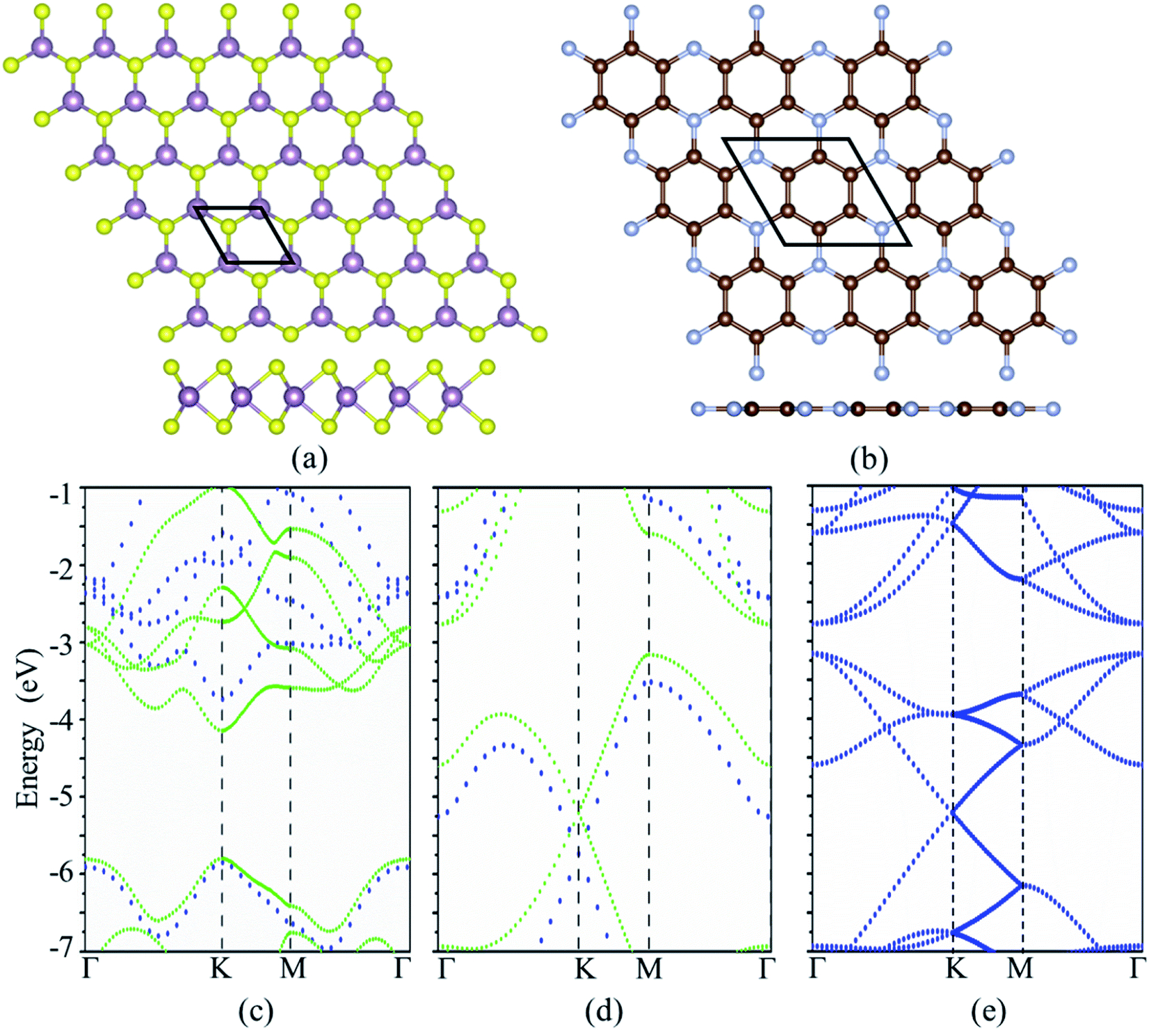 | ||
| Fig. 1 The top and side view of atomic configurations for (a) MoS2 and (b) C3N monolayers. The purple, yellow, brown and blue balls denote Mo, S, C, and N atoms, respectively. The band structures of (c) MoS2 and (d) C3N monolayers, the green and blue dotted lines represent the band structures calculated with standard DFT and the HSE functional, respectively. (e) Band structure of C3N monolayer calculated with 2 × 2 supercell. | ||
The most energy favorable stacking of MoS2/C3N heterostructure was evaluated by calculating the binding energy (Eb), Eb = Ehetero − EMoS2 − EC3N, where Ehetero, EMoS2, and EC3N are the total energies of heterostructure, MoS2, and C3N monolayers, respectively. The top and side views of possible stacking patterns are shown in Fig. 2, the binding energies and the interlayer distance are listed in Table 1. The calculated binding energies (Eb) are in the range between −15.086 and −15.114 meV Å−2, and the interlayer distance (d) between MoS2 and C3N monolayer in the heterostructures is in the range between 3.236 and 3.263 Å, which agrees well with reported typical values in vdW systems.41–44 These results indicate the weak vdW interaction between the two layers. The stacking configuration in Fig. 2c with one of the Mo atom of MoS2 monolayer coincide with a N atom of C3N monolayer has the largest negative binding energy, which indicates that this configuration is energy favorable. The following calculations are all based on this heterostructure.
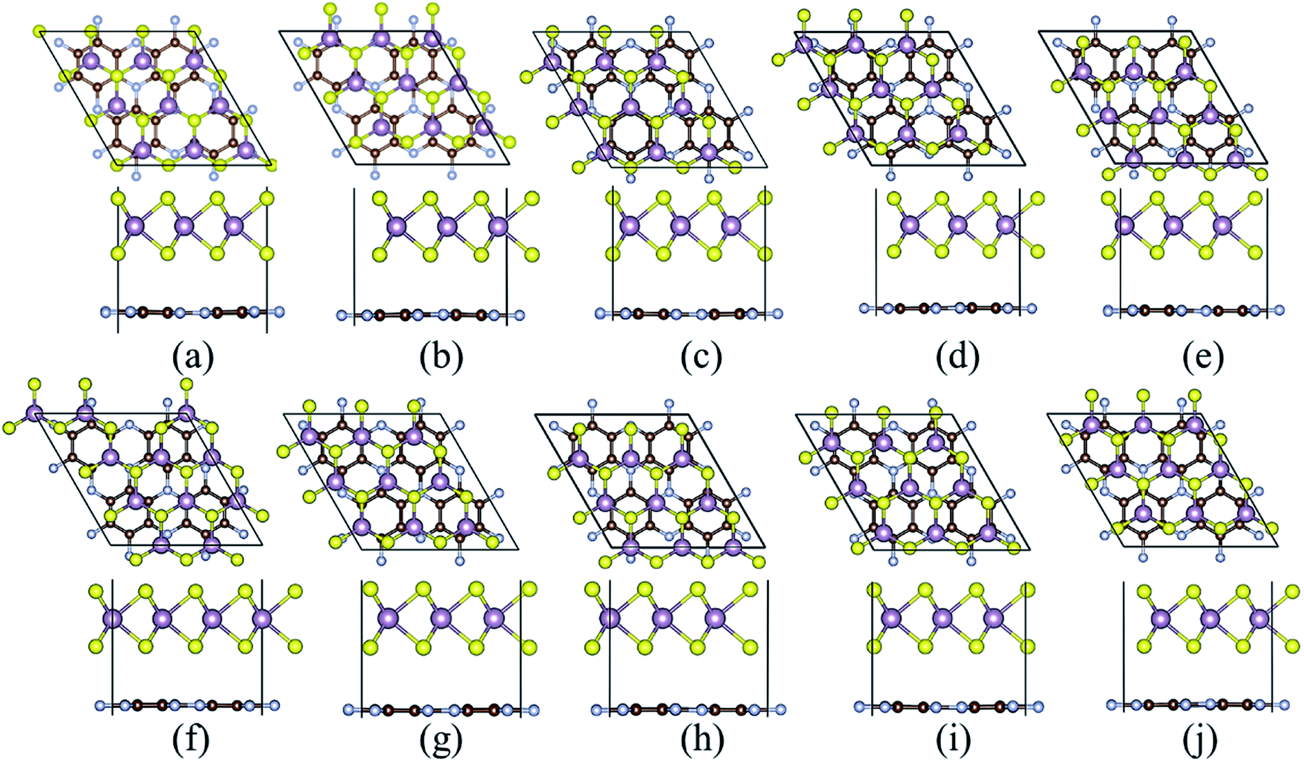 | ||
| Fig. 2 The atomic structures for the 2D vdW heterojunction in different configurations of arrangement of MoS2 monolayer on the top of C3N. The top column is the top view, and the bottom column is the side view. The purple, yellow, brown and blue, balls denote Mo, S, C, and N atoms, respectively. | ||
| a | b | c | d | e | f | g | h | i | j | |
|---|---|---|---|---|---|---|---|---|---|---|
| Eb | −15.110 | −15.112 | −15.114 | −15.103 | −15.086 | −15.106 | −15.103 | −15.096 | −15.110 | −15.110 |
| d | 3.236 | 3.263 | 3.246 | 3.261 | 3.259 | 3.254 | 3.256 | 3.262 | 3.254 | 3.251 |
The vdW heterostructures of MoS2 monolayer stacked on AlN (GaN) semiconductors has been well studied,45,46 and the band alignment can be tuned by varying the thickness of GaN. The work function can be used as an intrinsic reference for the band alignment. The work functions (energy difference between fermi energy level and vacuum level) of MoS2 monolayers are 5.66 and 5.79 eV calculated by standard DFT and HSE06 functional, respectively, which agree with the previous reports.47,48 The work functions of C3N monolayer are 2.93 eV and 3.39 eV calculated by standard DFT calculation and HSE06 functional, respectively. The calculated work function of C3N monolayer is smaller than that of MoS2 monolayers, which indicates that a broken gap vdW heterostructure may be formed for the MoS2/C3N heterostructure. The projected band structures of MoS2/C3N heterostructure were calculated with standard DFT and HSE functional and shown in Fig. 3a. The blue and orange dots represent the band contributions from C3N and MoS2 calculated with standard DFT, and the cane and green triangles represent those calculated by HSE06 functional, respectively. The corresponding band alignments calculated using standard DFT calculation and HSE functional are schematically shown in Fig. 3b and c, respectively. The MoS2 monolayer remains its direct band gap semiconducting property, but the band gap decrease from 1.65 eV of the pristine to 1.40 eV in the heterostructure. The decease of band gap of MoS2 monolayer has also observed in other heterostructures21 due to the interaction between the two monolayers.
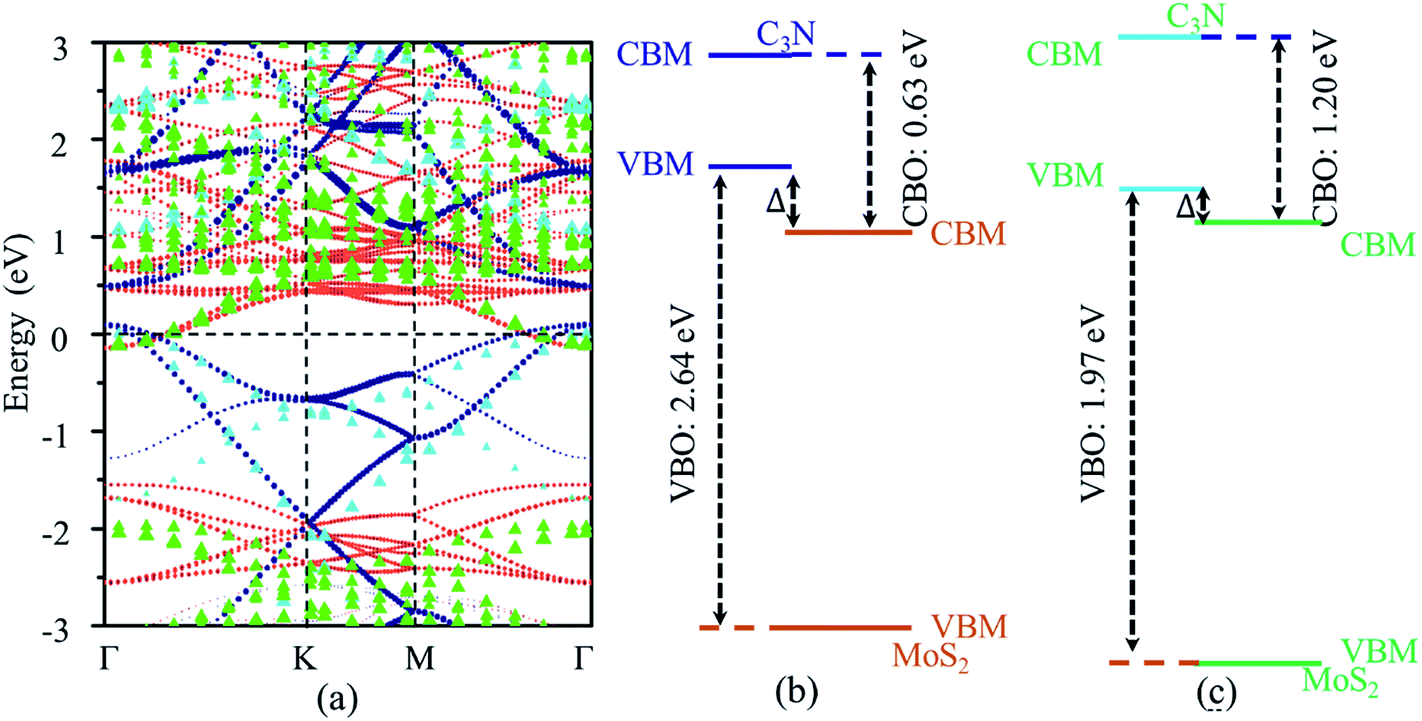 | ||
| Fig. 3 (a) Projected band structure and band alignment of MoS2/C3N heterojunction calculated with (b) standard DFT and (c) the HSE functional. The blue dots and orange dots represent the band contributions from C3N and MoS2 (calculated with standard DFT), and the cane and green triangular represent those calculated by the HSE functional, respectively. The dashed line represents the Fermi energy level. | ||
Both standard DFT and HSE06 calculations show that the VBM of C3N is higher than the CBM of MoS2. There is no overlap of the band gaps for MoS2 and C3N monolayers in the heterostructure, indicating the MoS2/C3N vdW heterostructure is with a type III alignment. For the standard DFT calculation, the conduction band offset (CBO) and valence band offset (VBO) are 0.63 and 2.64 eV, the band overlap  is 0.24 eV for the MoS2/C3N heterostructure. The CBO and VBO are 1.06 and 1.87 eV derived from the HSE06 calculation, and the band overlap is 0.12 eV. There exists considerable carrier migration in this sort of heterostructures even without an external electric field, it will lead to an accumulation of electrons in the MoS2 and holes in C3N near the junction. Under these circumstances, a highly doped p+/n+ heterojunction can be achieved in the MoS2/C3N heterostructure even without any electrostatic or chemical doping. This particular property makes it a promising material for negative differential resistance (NDR) devices.26,49
The electric field can be used to modulate the positions of VBM and CBM in 2D semiconductors, such as the CBM shifts to low energy as an external electric field applied perpendicular to the surface of GaGeTe monolayer.50 The electric field also can modify the band alignment of 2D heterostructures,26,28 such as a type II band alignment transforms to type III one as an the electric field is larger than 0.6 V Å−1 in MoTe2/WSe2 heterostructure.51 The effects of external electric field on the band alignment of MoS2/C3N heterostructure were investigated by applying positive (along the direction from MoS2 to C3N) and negative (along the direction from C3N to MoS2) electric field. The projected band structures of MoS2/C3N heterostructure with external electric field are plotted in Fig. 4a. As the negative electric field is changed from 0 to −0.4 V Å−1, the CBM of MoS2 and VBM of C3N shift upward and downward to the Fermi energy level, thus leading to the decrease in band overlap (Δ). The value of Δ is close to zero (0.004 eV) at an electric field of −0.2 V Å−1. Whereas the value of Δ increases as a positive electric field applied. The evolution of Δ with the electric field is shown in Fig. 4b. Δ increases from 0.24 to 0.33 eV as the positive electric field increases from 0 to 0.4 V Å−1. As can be seen from Fig. 4a, the CBM of MoS2 monolayer remains at the Γ point, while VBM shifts from Γ point to a point between Γ and K points as negative electric field applied. Both CBM and VBM remain at the Γ point as positive electric field applied. The positive electric field does not affect the position of CBM and VBM of C3N monolayer. The evolution of band gaps for MoS2 and C3N monolayers as a function of electric field is shown in Fig. 4c and d, respectively. The band gaps C3N monolayers decreases with the increase of negative electric field and increases with the positive electric field. While band gap of MoS2 changes a little with the electric field. These results indicate that the band structure and band alignment of MoS2/C3N heterostructure can be tuned by the external electric field, which can be used to tune the accumulation of holes in C3N and electrons in MoS2.
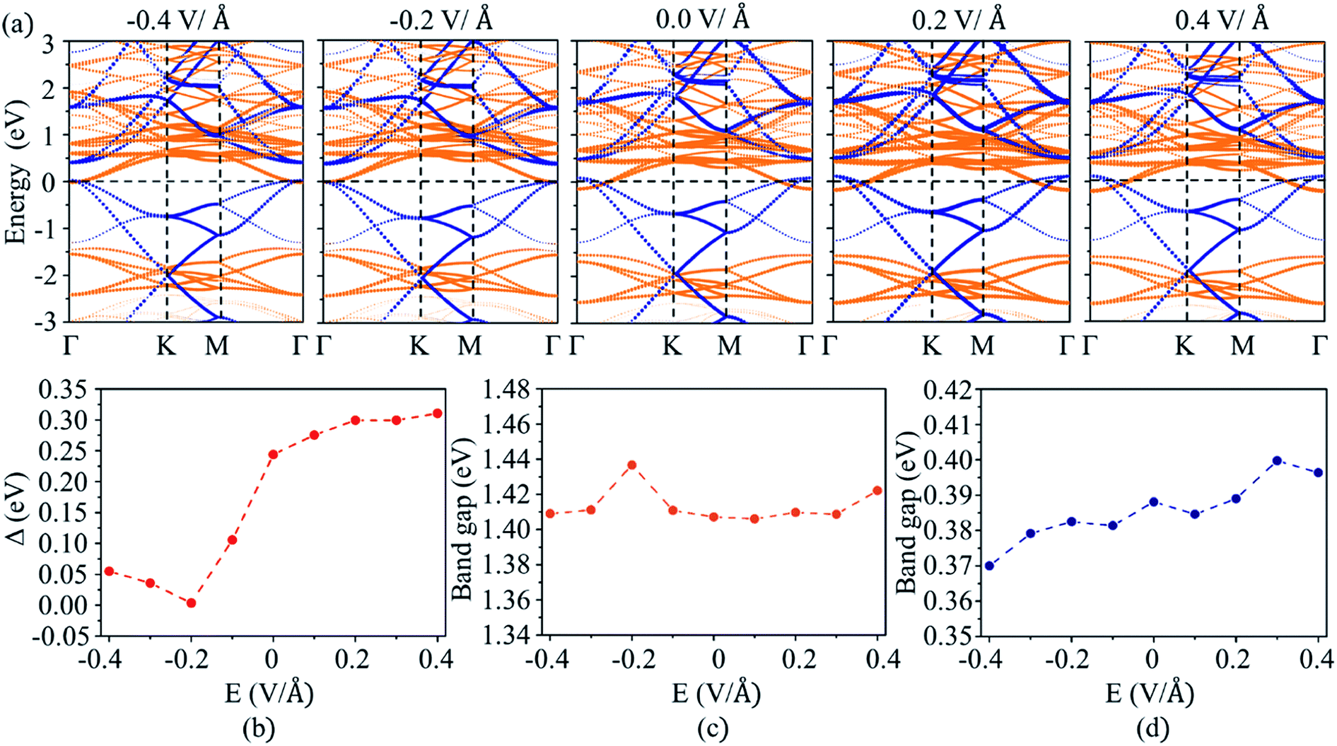 | ||
| Fig. 4 (a) The projected band structures of MoS2/C3N heterojunction with electric field applied. The blue dots and orange dots represent the band contributions from C3N and MoS2, respectively. Evolution of the (b) band overlap, band gap of (c) MoS2 and (d) C3N as a function of the external electric field. | ||
Except for the electric field, strain is often used to tune the electronic properties of 2D materials for meeting the requirements of application.37,52 The modulation of strain on the electric properties of MoS2/C3N heterostructure was investigated by applying the in-plane biaxial strain. The strain (ε) in the range between −4% and 8% is imposed by varying the lattice parameter with  where a and a0 are the lattice parameters of strain and pristine MoS2/C3N heterostructure. The projected band structures of MoS2/C3N heterostructure under strain are shown in Fig. 5a. As the tensile strain is increased from 0 to 8%, the value of Δ increases. When the strength of tensile strain is 6%, Δ reaching up to its maximum of 0.33 eV. The band overlap decreases with compressive strain as shown in Fig. 5a. As the compressive strain of −4% leads to band overlap very close to zero (0.0114 eV). Under tensile strain, the CBM of MoS2 was not changed by the strain, but the VBM of MoS2 moved upward with the increase in tensile strain, which leads the band gap decrease of MoS2. The compressive strain leads the CBM of MoS2 shifts to higher energy and VBM to lower energy, thus the band gap of MoS2 increases with increasing compressive strain as shown in Fig. 5c. Whereas the band gap of C3N monolayer increases with tensile strain or decreases with a compressive strain was applied, except for a large compressive strain of −4.0% (as shown in Fig. 5d). So the band alignment of MoS2/C3N heterostructure can also be tuned by applying a biaxial strain.
 | ||
| Fig. 5 (a) The projected band structures of MoS2/C3N heterojunction with strain applied. The blue dots and orange dots represents the band contributions from C3N and MoS2, respectively. Evolution of the (b) band overlap, band gap of (c) MoS2 and (d) C3N as a function of strain. | ||
The band alignment of MoS2/C3N heterostructure can be tuned by external vertical electric field and strain, and MoS2/C3N heterostructure keep the type III band alignment under all the studied conditions, thus the MoS2/C3N heterostructures is quite favorable for applications in tunneling devices based on the broken-gap heterostructures.
4. Conclusion
In conclusion, the structural and electronic properties of the MoS2/C3N heterostructure were studied using DFT calculation. The MoS2/C3N heterostructure is a broken-gap heterojunction with the VBM of C3N higher than the CBM of MoS2. The value of Δ increases from 0.24 to 0.33 eV as a positive electric field increases from 0 to 0.4 V Å−1. And the value of Δ decreases as a negative electric field is applied. The band overlap can also be tuned by bi-axil strain. Compressive strain induced the decrease of band overlap. The alignment type was not changed for both electric field and strain applied. The present work reveals that the MoS2/C3N heterostructures is quite favorable for applications in tunneling devices based on the broken-gap heterostructures.Conflicts of interest
There are no conflicts of interest to declare.References
- S. Hussain, K. Xu, S. Ye, L. Lei, X. Liu, R. Xu, L. Xie and Z. Cheng, Front. Phys., 2019, 14, 33401 CrossRef.
- K. Ren, M. Sun, Y. Luo, S. Wan, J. Yu and W. Tang, Appl. Surf. Sci., 2019, 476, 70–75 CrossRef CAS.
- W. Feng, Z. Jin, J. Yuan, J. Zhang, S. Jia, L. Dong, J. Yoon, L. Zhou, R. Vajtai, J. M. Tour, P. M. Ajayan, P. Hu and J. Lou, 2D Mater., 2018, 5, 025008 CrossRef.
- Y. Chen, X. Wang, G. Wu, Z. Wang, H. Fang, T. Lin, S. Sun, H. Shen, W. Hu, J. Wang, J. Sun, X. Meng and J. Chu, Small, 2018, 14, 1703293 CrossRef PubMed.
- A. Sengupta, A. Chanana and S. Mahapatra, AIP Adv., 2015, 5, 027101 CrossRef.
- M. Sun, P. Yang, D. Xie, Y. Sun, J. Xu, T. Ren and Y. Zhang, Adv. Electrode Mater., 2019, 5, 1800580 Search PubMed.
- H. Li, J. Wu, Z. Yin and H. Zhang, Acc. Chem. Res., 2014, 47, 1067–1075 CrossRef CAS PubMed.
- W. Su, H. Dou, J. Li, D. Huo, N. Dai and L. Yang, RSC Adv., 2015, 5, 82924–82929 RSC.
- M. Buscema, G. A. Steele, H. S. J. van der Zant and A. Castellanos-Gomez, Nano Res., 2014, 7, 561–571 CrossRef.
- W. Su, H. Dou, D. Huo, N. Dai and L. Yang, Chem. Phys. Lett., 2015, 635, 40–44 CrossRef CAS.
- S. Mouri, Y. Miyauchi and K. Matsuda, Nano Lett., 2013, 13, 5944–5948 CrossRef CAS PubMed.
- B. Mortazavi, Carbon, 2017, 118, 25–34 CrossRef CAS.
- X. Zhou, W. Feng, S. Guan, B. Fu, W. Su and Y. Yao, J. Mater. Res., 2017, 32, 2993–3001 CrossRef CAS.
- M. Makaremi, B. Mortazavi and C. V. Singh, J. Phys. Chem. C, 2017, 121, 18575–18583 CrossRef CAS.
- Y. Deng, Z. Luo, N. J. Conrad, H. Liu, Y. Gong, S. Najmaei, P. M. Ajayan, J. Lou, X. Xu and P. D. Ye, ACS Nano, 2014, 8, 8292–8299 CrossRef CAS PubMed.
- J. Yan, Y. Hao, Y. Cui, J. Zhang, Y. Zou, W. Zhang, G. Yu, J. Zheng, W. Xu and D. Zhu, J. Mater. Chem. C, 2018, 6, 12976–12980 RSC.
- K. H. Chan, S. M. Ng, H. F. Wong, C. W. Leung and C. L. Mak, Phys. Status Solidi A, 2019, 216, 1800829 CrossRef.
- K. Tang, W. Qi, Y. Li and T. Wang, Phys. Chem. Chem. Phys., 2018, 20, 29333–29340 RSC.
- Q. Qiao, K. Yang, L. L. Ma, W. Q. Huang, B. X. Zhou, A. Pan, W. Hu, X. Fan and G. F. Huang, J. Phys. D, 2018, 51, 275302 CrossRef.
- S. S. Ding, W. Q. Huang, Y. C. Yang, B. X. Zhou, W. Y. Hu, M. Q. Long, P. Peng and G. F. Huang, J. Appl. Phys., 2016, 119, 205704 CrossRef.
- C. Liao, Y. Zhao and G. Ouyang, ACS Omega, 2018, 3, 14641–14649 CrossRef CAS.
- J. Shim, S. Oh, D. H. Kang, S. H. Jo, M. H. Ali, W. Y. Choi, K. Heo, J. Jeon, S. Lee, M. Kim, Y. J. Song and J. H. Park, Nat. Commun., 2016, 7, 13413 CrossRef CAS PubMed.
- M. Yagmurcukardes, E. Torun, R. T. Senger, F. M. Peeters and H. Sahin, Phys. Rev. B, 2016, 94, 195403 CrossRef.
- C. Grillet, A. Cresti and M. G. Pala, IEEE Trans. Electron Devices, 2018, 65, 3038–3044 CAS.
- S. Alagha, S. Zhao, Z. Mi, S. P. Watkins and K. L. Kavanagh, IEEE Trans. Electron Devices, 2018, 33, 015008 Search PubMed.
- R. Yan, S. Fathipour, Y. Han, B. Song, S. Xiao, M. Li, N. Ma, V. Protasenko, D. A. Muller, D. Jena and H. G. Xing, Nano Lett., 2015, 15, 5791–5798 CrossRef CAS PubMed.
- J. Shim, D. H. Kang, Y. Kim, H. Kum, W. Kong, S. H. Bae, I. Almansouri, K. Lee, J. H. Park and J. Kim, Carbon, 2018, 133, 78–89 CrossRef CAS.
- J. Shi, Y. Ou, M. A. Mighorato, H. Wang, H. Li, Y. Zhang, Y. Gu and M. Zou, Comput. Mater. Sci., 2019, 160, 301–308 CrossRef CAS.
- P. J. Stephens, F. J. Devlin, C. F. Chabalowski and M. J. Frisch, J. Phys. Chem., 1994, 98, 11623–11627 CrossRef CAS.
- M. Brandbyge, J. L. Mozos, P. Ordejon, J. Taylor and K. Stokbro, Phys. Rev. B: Condens. Matter Mater. Phys., 2002, 65, 165401 CrossRef.
- G. Kresse and D. Joubert, Phys. Rev. B: Condens. Matter Mater. Phys., 1999, 59, 1758–1775 CrossRef CAS.
- H. J. Monkhorst and J. D. Pack, Phys. Rev. B: Solid State, 1976, 13, 5188–5192 CrossRef.
- M. B. Tagani, Comput. Mater. Sci., 2018, 153, 126–133 CrossRef CAS.
- A. Slassi and J. Cornil, 2D Mater., 2018, 6, 015025 CrossRef.
- K. F. Mak, C. Lee, J. Hone, J. Shan and T. F. Heinz, Phys. Rev. Lett., 2010, 105, 136805 CrossRef PubMed.
- J. Heyd, G. E. Scuseria and M. Ernzerhof, J. Chem. Phys., 2003, 118, 8207–8215 CrossRef CAS.
- L. B. Shi, M. B. Li, X. M. Xiu, X. Y. Liu, K. C. Zhang, Y. H. Liu, C. R. Li and H. K. Dong, J. Appl. Phys., 2017, 121, 205305 CrossRef.
- X. Wang, Q. Li, H. Wang, Y. Gao, J. Hou and J. Shao, Phys. B, 2018, 537, 314–319 CrossRef CAS.
- L. Xie, L. Yang, W. Ge, X. Wang and J. Jiang, Chem. Phys., 2019, 520, 40–46 CrossRef CAS.
- X. Gao, Y. Shen, Y. Ma, S. Wu and Z. Zhou, Appl. Surf. Sci., 2019, 479, 1098–1104 CrossRef CAS.
- T. Bjorkman, A. Gulans, A. V. Krasheninnikov and R. M. Nieminen, Phys. Rev. Lett., 2012, 108, 235502 CrossRef CAS PubMed.
- T. Bjorkman, A. Gulans, A. V. Krasheninnikov and R. M. Nieminen, J. Phys.: Condens. Matter, 2012, 24, 424218 CrossRef CAS PubMed.
- Y. C. Yang, L. Xu, W. Q. Huang, C. Y. Luo, G. F. Huang and P. Peng, J. Phys. Chem. C, 2015, 119, 19095–19104 CrossRef CAS.
- C. F. Fu, R. Zhang, Q. Luo, X. Li and J. Yang, J. Comput. Chem., 2019, 40, 980–987 CrossRef CAS PubMed.
- J. Liao, B. Sa, J. Zhou, R. Ahuja and Z. Sun, J. Phys. Chem. C, 2014, 118, 17594–17599 CrossRef CAS.
- J. Wang, H. Shu, P. Liang, N. Wang, D. Cao and X. Chen, J. Phys. Chem. C, 2019, 123, 3861–3867 CrossRef CAS.
- P. Wu, M. Huang, N. Yin and P. Li, Nanomaterials, 2019, 9, 395 CrossRef PubMed.
- S. Kwon, S. H. Choi, Y. J. Kim, I. T. Yoon and W. Yang, Thin Solid Films, 2018, 660, 766–770 CrossRef CAS.
- H. Kroemer, Phys. Scr., 1996, T68, 10–16 CrossRef CAS.
- C. Ke, Y. Wu, J. Zhou, Z. Wu, C. Zhang, X. Li and J. Kang, J. Phys. D, 2019, 52, 115101 CrossRef.
- Y. Liu and X. Cheng, Phys. E, 2019, 108, 90–95 CrossRef CAS.
- H. Aramberri and M. C. Munoz, Phys. Rev. B, 2017, 95, 205422 CrossRef.
| This journal is © The Royal Society of Chemistry 2019 |