DOI:
10.1039/C9RA02855B
(Paper)
RSC Adv., 2019,
9, 22124-22128
Flexible carbon nanotube Schottky diode and its integrated circuit applications
Received
16th April 2019
, Accepted 8th July 2019
First published on 16th July 2019
Abstract
Carbon nanotubes (CNTs), a low-dimensional material currently popular in industry and academia, are promising candidates for addressing the limits of existing semiconductors. In particular, CNTs are attractive candidates for flexible electronic materials due to their excellent flexibility and potential applications. In this work, we demonstrate a flexible CNT Schottky diode based on highly purified, preseparated, solution-processed 99% semiconducting CNTs and an integrated circuit application using the CNT Schottky diodes. Notably, the fabricated flexible CNT diode can greatly modulate the properties of the contact formed between the semiconducting CNT and the anode electrode via the control gate bias, exhibiting a high rectification ratio of up to 2.5 × 10⁵. In addition, we confirm that the electrical performance of the CNT Schottky diodes does not significantly change after a few thousand bending/releasing cycles of the flexible substrate. Finally, integrated circuit (IC) applications of logic circuits (OR and AND gates) and an analog circuit (a half-wave rectifier) were presented through the use of flexible CNT Schottky diode combinations. The correct output responses are successfully achieved from the circuit applications; hence, we expect that our findings will provide a promising basis for electronic circuit applications based on CNTs.
Introduction
Low-dimensional semiconducting materials have attracted tremendous interest in industry and been extensively studied over the past few years. One low-dimensional material, carbon nanotubes (CNTs), is attracting attention for use in flexible electronics due to its excellent electrical and mechanical properties.1–5 In particular, highly purified semiconducting CNTs have been considered an excellent material for building high-performance diodes, field-effect transistors (FETs), and thin-film transistors (TFTs) for future applications in integrated circuits (ICs).6–10 Among these applications, diodes constitute the basic building blocks of modern micro- and nanoelectronics and can simply implement most logic functions and analog circuits, such as diode-based logic circuits, rectifiers, clamps, and multipliers. A key feature of diodes is their well-known rectifying behavior, i.e., extremely asymmetric current–voltage characteristics under forward and reverse bias.11 Typically, CNT-based devices exhibit p-type operation in ambient conditions, making the implementation of CNT-based pn junction diodes difficult. Thus, many researchers have attempted to convert p-type CNTs into n-type CNTs through chemical and electrostatic doping.12–17 However, these doping techniques still have several issues in terms of controllability and stability. One way to solve the abovementioned issues is to fabricate a Schottky contact through the work function design of the electrodes in contact to the semiconducting CNTs. Various Schottky diodes based on CNTs have been recently reported, such as gated diodes,18,19 radio frequency diodes,20 and diodes for IC applications.21–23 Among those reports, flexible Schottky diodes based on semiconducting CNTs have been used as radio frequency circuit applications.23 However, to the best of our knowledge, there have been no studies on flexible Schottky diodes with an embedded control gate to improve the electrical performance.
The present work demonstrates a flexible Schottky diode based on highly purified, preseparated, solution-processed 99% semiconducting CNTs obtained from a density-gradient ultracentrifugation method.24,25 This high-purity semiconducting CNT enables the realization of a high device yield; hence, the fabrication of various ICs based on the CNTs is possible. Our flexible CNT Schottky diode consists of two Schottky rectifying and ohmic contacts with asymmetric titanium (Ti) cathode and palladium (Pd) anode electrodes, respectively. In addition, the Pd local bottom gate is used as an embedded control gate to modulate the properties of the contact and further improve the rectification ratio (i.e., the forward/reverse diode current ratio) of the CNT Schottky diodes. Our flexible CNT Schottky diodes exhibit nearly ideal diode characteristics, yielding a high rectification ratio of over 105. Using a flexible CNT Schottky diode with these advantages, we demonstrate diode logic gates (OR and AND gates) and an analog circuit (a half-wave rectifier). Both the logic gates and the analog circuit made of flexible CNT Schottky diodes show the correct logic functions according to the input signal using the control gate. Therefore, we believe that concept and results shown in this work will be representative work for the further development of flexible electronics and ICs.
Results and discussion
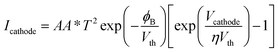
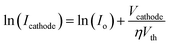
Fig. 1a shows graphical illustrations of the flexible Schottky diode based on a semiconducting CNT network with an embedded control gate. For diode fabrication, highly purified, preseparated 99% semiconducting CNTs were used to form percolated networks. The fabrication process started with a poly(ethylene terephthalate) (PET) substrate with a 50 nm thick silicon dioxide (SiO2) layer as the buffer layer. The local bottom control gate was then formed from Ti and Pd layers with a thickness of 2/30 nm on the buffer layer using electron beam (e-beam) evaporation. Next, an aluminum oxide (Al2O3) film was grown through atomic layer deposition (ALD) at 80 °C, followed by the deposition of a thin SiO2 film using e-beam evaporation for CNT network formation. The substrate was then cleaned with oxygen plasma treatment, and a poly-L-lysine solution (0.1% w/v in water; Sigma Aldrich) was dropped onto the substrate surface. The poly-L-lysine solution functionalizes the substrate by introducing an amine-terminated surface to effectively adhere the semiconducting CNT networks.26–28 The substrate was thoroughly rinsed with deionized (DI) water and dried with flowing nitrogen gases. The percolated CNT network was subsequently formed by immersing the chip into a commercially available 0.01 mg mL−1 99% semiconducting CNT solution (purchased from NanoIntegris Inc.) for several minutes and rinsing the chip thoroughly with DI water and isopropanol. Afterward, Ti and Pd layers (2 and 30 nm, respectively) were patterned by photolithography and evaporated to form the anode electrodes for ohmic contact because Pd can form good ohmic contact with semiconducting CNTs.29,30 Sequentially, Ti, as a cathode electrode, was deposited to form a Schottky rectifying contact with the CNTs, followed by a lift-off process. Finally, an oxygen plasma-etching step was performed to remove any unwanted pathways from the CNTs to outside the diode region, and the CNT Schottky diode with a control gate was completed. Fig. 1b shows a micrograph of a flexible CNT Schottky diode with an embedded control gate fabricated on a PET substrate. Fig. 1c exhibits the photograph of flexible CNT Schottky diodes fabricated onto a PET film being bent. An atomic force microscopy (AFM) image of the percolated CNT network constructed from the 99% semiconducting CNT solution is also shown in Fig. 1d. The percolated CNT network film exhibits good uniformity, with an average CNT density of 82 ± 3 tubes per μm2 over a large area.
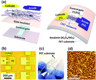 |
| | Fig. 1 (a) Schematic diagram of the flexible CNT Schottky diode with Ti as the cathode, Pd as the anode, and Ti/Pd as the embedded control gate. (b) Optical micrograph of the fabricated CNT Schottky diode on a PET substrate. (c) Optical image of the flexible CNT diode on a PET substrate. (d) AFM image (2.5 × 2.5 μm, the z-scale is 10 nm) of the CNT network channel constructed from a 99% semiconducting CNT solution. | |
The electrical characteristics (i.e., cathode current Icathode vs. cathode voltage Vcathode) of the fabricated flexible CNT diodes were measured for various control gate voltages (VCG) in an ambient state, and the Icathode–Vcathode characteristics of the diodes exhibited typical diode rectification behavior, as shown in Fig. 2a. Our flexible CNT diode is a metal–semiconductor–metal structure and has two different metal–semiconductor contacts: one is an ohmic contact, and the other is a rectifying contact. The current in the rectifying contact is based on thermionic emission and can be expressed as11
| |
 | (1) |
where
A is the junction area of the diode,
A* is the Richardson constant,
Vth is the thermal voltage,
ϕB is the Schottky-barrier height, and
η is the ideality factor of Schottky diodes. In our diode, the Schottky rectifying behavior occurs at the contact between semiconducting CNTs and the Ti electrode. Importantly, it is observed that, as the
VCG value was increased negatively,
Icathode was significantly increased, with the
η of the CNT diodes approaching 2.3. The
η was calculated from the following equation:
| |
 | (2) |
where
Io is the reverse saturation current of the diode (
Io =
AA*
T2![[thin space (1/6-em)]](https://www.rsc.org/images/entities/char_2009.gif)
exp(−
ϕB/
Vth)). The
η of the fabricated CNT diode in
eqn (2) can be extracted from the intercept of the linear fit to the diode current log-scale plot. For the normal case, the junction between the semiconducting CNTs and the Pd electrode is known to be an ohmic contact due to high workfunction of Pd electrode. However, the potential barrier formed between the semiconducting CNTs and the Pd electrode can further be modulated by the control gate bias; hence, the electrical characteristics of the CNT Schottky diode can be adjusted.
Fig. 2b illustrates the operation principle of the proposed CNT Schottky diode through the energy band diagram at different
VCG polarities. First, as the
VCG value more increases negatively, additional majority-carrier holes are injected from the Pd electrode
via thermionic emission because the potential barrier at the interface between the semiconducting CNTs and Pd metal is controlled and further reduced; therefore, the forward
Icathode can be increased. On the contrary, when the
VCG value increases positively, the potential barrier increases from the view point of the rectifying operation, which makes the supply of majority-carrier holes very difficult; as a result, the characteristics of the Schottky diode are almost lost.
Fig. 2c shows a histogram of the on-state current (
ION) defined at
Vcathode = −3 V and the off-state current (
IOFF) defined at
Vcathode = +1 V from
VCG = −8 V to +8 V, showing that the control gate causes a large change in the
ION of the CNT Schottky diode. Thus, it is expected that the modulation of the diode functions through the control gate facilitates the performance enhancement of the diode-based logic gates and analog circuit functions.
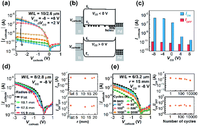 |
| | Fig. 2 (a) The electrical characteristics (Icathode–Vcathode) of the flexible CNT Schottky diode with Pd (anode) and Ti (cathode) electrodes. (b) The operational principle of the proposed CNT diode at different VCG polarities. (c) Histogram of ION and IOFF for different VCG values in the fabricated CNT diode. (d) Electrical characteristics and comparison of ION and ION/IOFF under three different bending conditions (r = 19.1 mm, 17.5 mm, and 11.9 mm); (e) electrical characteristics and comparison of ION and ION/IOFF after 1, 10, 50, 100, 500, 1000, and 5000 measurement cycles for the flexible CNT diodes measured at VCG = −8 V. | |
To characterize the mechanical flexibility of our CNT Schottky diodes consisting of 99% semiconducting CNTs, we also evaluated their electrical properties under various degrees of bending. For each measurement, the CNT Schottky diodes were fixed on different types of rods with different radii of curvature: r = 19.1 mm, 17.5 mm, and 11.9 mm. Fig. 2d shows the measured Icathode–Vcathode at VCG = −8 V for the CNT diodes at the abovementioned degrees of bending. Although there was a slight reduction in ION and ION/IOFF due to the slight morphological variation in the percolated CNT network,31,32 no serious degradation in device performance was observed. We also tested the stability of our flexible CNT diodes for more than 5000 bending/releasing cycles (r = 15 mm), and the results are shown in Fig. 2e. ION and ION/IOFF remained nearly unchanged up to 1000 cycles, but the device characteristics deteriorated at 5000 cycles. The above results suggest that the proposed CNT diode exhibits sufficient stability and reliability and shows potential for use in large-area flexible electronics.
Although diodes can be used as building blocks to construct various digital and analog circuits, diode-based integrated circuits are rarely realized in CNT due to the low yield and poor stability of CNT devices. However, in this paper, because of the advantages of the highly purified, solution-processed 99% semiconducting CNTs suggested, we are able to fabricated flexible Schottky diodes with high yield and high stability, which indeed make it possible to construct diode-based integrated circuits. First, as representative fundamental logic gates, OR and AND gates were simply constructed with two Schottky diodes and one external load resistance (RL = 1 GΩ), as shown in the equivalent circuits of Fig. 3a. The difference between the diode-based OR and AND gates was merely that the positions of the cathode and anode electrodes were changed. Fig. 3b shows the input signal and output response characteristics of the OR and AND logic gates for VCG with different values of −8 V, 0 V, and +8 V. Input voltages (VA and VB) with a square wave and a peak-to-peak (VPP) value of 1 V were injected, and the output voltage (VOUT) was simultaneously measured. When a VCG of 0 V was applied, both logic gates at a supply voltage (VDD) of 1 V showed incomplete output signals but still performed OR and AND logic functions. In addition, when negative VCG values (i.e., −8 V) were applied, total resistance of the CNT diode decreased by further reducing the potential barrier as aforementioned, and the voltage drop across RL increased; thus, the output responses presented more correct and accurate logic functions. In contrast, when a positive VCG (i.e., +8 V) was applied, the digital logic functionality was lost due to the deteriorated diode characteristics. The control gate contributes to the performance improvements of the CNT Schottky diode and provides a more accurate output signal in the CNT diode-based logic.
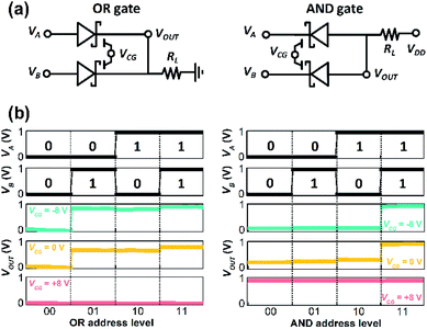 |
| | Fig. 3 (a) Equivalent circuits and (b) output responses of the OR and AND logic gates with two flexible CNT Schottky diodes for VCG values of −8 V, 0 V, and +8 V. | |
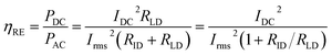
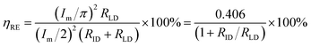
Diodes can be implemented in analog circuits in addition to their wide use in digital logic circuits, especially rectifier circuits. We demonstrate a half-wave rectifier using two CNT diodes, as shown in Fig. 4a. A half-wave rectifier is a circuit in which either the positive half or the negative half of an alternating current (AC) wave is passed, while the other half is blocked; it is mainly used to convert AC input power to direct current (DC) output power. The implemented half-wave rectifier had a sinusoidal AC input signal of 1 V VPP, and VOUT was observed for different VCG values, as shown in Fig. 4b. Exhibiting the same tendency as the diode-logic gates, the output response characteristics were improved when the VCG value in the half-wave rectifier was increased negatively, and the output responses became correct with almost no loss of the peak voltage of 0.94 V. Compared with the case in which the output peak voltage was 0.69 V at VCG = 0 V, the output peak voltage increased by 36%. With these results, we can calculate the rectifier efficiency (ηRE) of our half-wave rectifier. ηRE is defined as the ratio of useful output power (DC power) to AC input power, which is given by21,33
| |
 | (3) |
where
IDC is the DC current value flowing through the load diode,
Irms is the effective AC current value flowing through the load diode,
RID is the dynamic resistance of the input stage diode, and
RLD is the dynamic resistance of the load diode. For a half-wave rectifier,
eqn (3) can be summarized as follows:
21,33| |
 | (4) |
where
Im is the maximum current value flowing through
RLD. According to
eqn (4), the ideal
ηRE of a half-wave rectifier is 40.6%. The extracted
ηRE value of our CNT Schottky diode-based half-wave rectifier at a
VCG of −8 V was 39.3%; that is, the implemented half-wave rectifier showed performance close to the ideal
ηRE. Therefore, we believe that our research will be an important foundation for future applications of integrated CNT-based nanoelectronics or key components of radio frequency circuits.
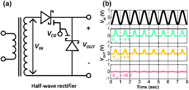 |
| | Fig. 4 (a) Circuit diagram and (b) sequential measurement results of a half-wave rectifier circuit with two flexible CNT Schottky diodes for VCG values of −8 V, 0 V, and +8 V. | |
Conclusions
We demonstrated the flexible Schottky diode based on the 99% semiconductor-enriched nanotubes. Notably, the proposed flexible CNT Schottky diodes showed improved performance through the control gate bias. The fabricated flexible CNT diode exhibited high operational stability and high device yield without significant deterioration during the mechanical bending test. Using these predictable and reproducible high-performance CNT Schottky diodes, we implemented various IC applications, such as digital logic gates and analog circuits. By applying a negative VCG, the output response of the digital and analog circuits resulted in a more accurate logic function for the input signal. This approach can eliminate complicated manufacturing issues for versatile functional devices. As excellent performance was achieved with the circuits, we believe that the flexible CNT diode will be an important step toward the realization of ICs.
Conflicts of interest
There are no conflicts to declare.
Acknowledgements
This work was supported by the National Research Foundation (NRF) of Korea under grants 2019R1A2B5B01069988 and 2016R1A5A1012966 and by the Future Semiconductor Device Technology Development Program (Grant 10067739) funded by MOTIE (Ministry of Trade, Industry & Energy) and KSRC (Korea Semiconductor Research Consortium).
Notes and references
- L. Cai, S. Zhang, J. Miao, Z. Yu and C. Wang, ACS Nano, 2016, 10, 11459–11468 CrossRef CAS.
- M. Yu, H. Wan, L. Cai, J. Miao, S. Zhang and C. Wang, ACS Nano, 2018, 12, 11572–11578 CrossRef CAS.
- J. B. Andrews, J. A. Cardenas, C. J. Lim, S. G. Noyce, J. Mullett and A. D. Franklin, IEEE Sens. J., 2018, 18, 7875–7880 CAS.
- S.-J. Park, J. Kim, M. Chu and M. Khine, Adv. Mater. Technol., 2018, 3, 1700158 CrossRef.
- L. Nela, J. Tang, Q. Cao, G. Tulevski and S.-J. Han, Nano Lett., 2018, 18, 2054–2059 CrossRef CAS.
- C. Zhao, D. Zhong, J. Han, L. Liu, Z. Zhang and L.-M. Peng, Adv. Funct. Mater., 2019, 1, 1808574 CrossRef.
- H. Zhang, L. Xiang, Y. Yang, M. Xiao, J. Han, L. Ding, Z. Zhang, Y. Hu and L.-M. Peng, ACS Nano, 2018, 12, 2773–2779 CrossRef CAS.
- D. Zhong, Z. Zhang, L. Ding, J. Han, M. Xiao, J. Si, L. Xu, C. Qiu and L.-M. Peng, Nat. Electron., 2018, 1, 40–45 CrossRef CAS.
- B.-W. Wang, S. Jiang, Q.-B. Zhu, Y. Sun, J. Luan, P.-X. Hou, S. Qiu, Q.-W. Li, C. Liu, D.-M. Sun and H.-M. Cheng, Adv. Mater., 2018, 30, 1802057 CrossRef.
- X. Cao, F. Wu, C. Lau, Y. Liu, Q. Liu and C. Zhou, ACS Nano, 2017, 11, 2008–2014 CrossRef CAS.
- S. M. Sze and K. K. Ng, Physics of Semiconductor Devices, John Wiley & Sons, Hoboken, 2006, ch. 2, p. 91 Search PubMed.
- Y. Yang, L. Ding, J. Han, Z. Zhang and L.-M. Peng, ACS Nano, 2017, 11, 4124–4132 CrossRef CAS.
- J. Lee, J. Yoon, B. Choi, D. Lee, D. M. Kim, D. H. Kim, Y.-K. Choi and S.-J. Choi, Appl. Phys. Lett., 2016, 109, 263103 CrossRef.
- J. Zhang, C. Wang, Y. Fu, Y. Che and C. Zhou, ACS Nano, 2011, 5, 3284–3292 CrossRef CAS.
- A. Javey, H. Kim, M. Brink, Q. Wang, A. Ural, J. Guo, P. McIntyre, P. McEuen, M. Lundstrom and H. Dai, Nat. Mater., 2002, 1, 241–246 CrossRef CAS.
- T.-J. Ha, K. Chen, S. Chuang, K. M. Yu, D. Kiriya and A. Javey, Nano Lett., 2015, 15, 392–397 CrossRef CAS.
- D. Shahrjerdi, A. D. Franklin, S. Oida, J. A. Ott, G. S. Tulevski and W. Haensch, ACS Nano, 2013, 7, 8303–8308 CrossRef CAS.
- M. A. Hughes, K. P. Homewood, R. J. Curry, Y. Ohno and T. Mizutani, Appl. Phys. Lett., 2013, 103, 133508 CrossRef.
- M. H. Yang, K. B. K. Teo, W. I. Milne and D. G. Hasko, Appl. Phys. Lett., 2005, 87, 253116 CrossRef.
- H. M. Manohara, E. W. Wong, E. Schlecht, B. D. Hunt and P. H. Siegel, Nano Lett., 2005, 5, 1469–1474 CrossRef CAS.
- J. Si, L. Liu, F. Wang, Z. Zhang and L.-M. Peng, ACS Nano, 2016, 10, 6737–6743 CrossRef CAS.
- Y. Zhao, X. Xiao, Y. Huo, Y. Wang, T. Zhang, K. Jiang, J. Wang, S. Fan and Q. Li, ACS Appl. Mater. Interfaces, 2017, 9, 18945–18955 CrossRef CAS.
- A. Kaur, X. Yang and P. Chahal, IEEE Trans. Compon., Packag., Manuf. Technol., 2016, 6, 1766–1775 CAS.
- M. S. Arnold, A. A. Green, J. F. Hulvat, S. I. Stupp and M. C. Hersam, Nat. Nanotechnol., 2006, 1, 60–65 CrossRef CAS.
- M. S. Arnold, S. I. Stupp and M. C. Hersam, Nano Lett., 2005, 5, 713–718 CrossRef CAS PubMed.
- J. Zhang, C. Wang and C. Zhou, ACS Nano, 2012, 6, 7412–7419 CrossRef CAS.
- J. Yoon, J. Han, B. Choi, Y. Lee, Y. Kim, J. Park, M. Lim, M.-H. Kang, D. H. Kim, D. M. Kim, S. Kim and S.-J. Choi, ACS Nano, 2018, 12, 6006–6012 CrossRef CAS.
- Y. Lee, J. Yoon, B. Choi, H. Lee, J. Park, M. Jeon, J. Han, J. Lee, Y. Kim, D. H. Kim, D. M. Kim and S.-J. Choi, Appl. Phys. Lett., 2017, 111, 173108 CrossRef.
- A. Javey, J. Guo, Q. Wang, M. Lundstrom and H. Dai, Nature, 2003, 424, 654–657 CrossRef CAS.
- A. Javey, J. Guo, D. B. Farmer, Q. Wang, D. Wang, R. G. Gordon, M. Lundstrom and H. Dai, Nano Lett., 2004, 4, 447–450 CrossRef CAS.
- Y. Lee, B. Choi, J. Yoon, Y. Kim, J. Park, H.-J. Kim, D. H. Kim, D. M. Kim, S. Kim and S.-J. Choi, AIP Adv., 2018, 8, 065109 CrossRef.
- J. Lee, M. Lim, J. Yoon, M. S. Kim, B. Choi, D. M. Kim, D. H. Kim, I. Park and S.-J. Choi, ACS Appl. Mater. Interfaces, 2017, 9, 26279–26285 CrossRef CAS PubMed.
- B. Paul, Industrial Electronics and Control: Including Programmable Logic Controller, Rajkamal Electric Press, Sonipat, Haryana, 2014, ch. 1, p. 2 Search PubMed.
|
| This journal is © The Royal Society of Chemistry 2019 |
Click here to see how this site uses Cookies. View our privacy policy here. 
 Open Access Article
 This Open Access Article is licensed under a Creative Commons Attribution-Non Commercial 3.0 Unported Licence
 *a
*a


