
 Open Access Article
 This Open Access Article is licensed under a Creative Commons Attribution-Non Commercial 3.0 Unported Licence
Highly uniform monolayer graphene synthesis via a facile pretreatment of copper catalyst substrates using an ammonium persulfate solution†
Hyunhak Jeong‡
ab,
Wang-Taek Hwang‡a,
Younggul Songa,
Jae-Keun Kima,
Youngrok Kima,
Joshua Hihathb,
Seungjun Chung*c and
Takhee Lee *a
*a
aDepartment of Physics and Astronomy, Institute of Applied Physics, Seoul National University, Seoul 08826, South Korea. E-mail: tlee@snu.ac.kr
bElectrical and Computer Engineering, University of California, Davis, CA 95616, USA
cPhoto-Electronic Hybrids Research Center, Korea Institute of Science and Technology (KIST), Seoul 02792, South Korea. E-mail: seungjun@kist.re.kr
First published on 3rd July 2019
Abstract
The demand for large-area, high-quality synthesis of graphene with chemical vapor deposition (CVD) has increased for the realization of next-generation transparent and flexible optoelectronic applications. In conventional CVD processes, various synthesis parameters can strongly affect the quality of the resultant graphene. In particular, surface engineering of a copper catalyst substrate is one of the most promising pathways for achieving high-quality graphene with excellent reproducibility. For this purpose, simple wet chemical etching of a catalyst substrate without toxic fume byproducts or metal ion residues is desired. Here, we suggest a facile method for preparing a pretreated copper catalyst substrate for highly uniform, large-area CVD graphene growth. This pretreatment method involves a wet copper etchant, ammonium persulfate (APS) solution, and gentle ultrasonication (100 W), which do not produce unwanted or toxic fume byproducts during their reaction. Moreover, this approach does not leave metal ion residue on the cleaned copper substrates that serves as residual nucleation sites and leads to multilayer graphene growth. To evaluate the quality of the synthesized monolayer graphene on the cleaned copper catalyst substrates, we used various characterization techniques, such as Raman spectroscopy and sheet resistance, optical transmittance, and FET characterization.
1. Introduction
Graphene, which is a two-dimensional honeycomb lattice of sp2-hybridized carbon atoms, has attracted much attention since the first successful separation and characterization of single-layer graphene in 2004.1 In particular, its promising intrinsic properties, such as a high carrier mobility, robust mechanical tolerance and high optical transparency,2,3 provide great opportunities for utilization in future ultimate scale device applications. Therefore, many research groups have proposed several approaches, such as chemical exfoliation, epitaxial growth, pyrolysis, and chemical vapor deposition (CVD), for preparing large-area and high-quality graphene.4,5 Among these processes, CVD growth of graphene using a metal catalyst is one of the most relevant methods due to its capability with mass production of graphene beyond laboratory-scale applications.6 As a metal catalyst, a copper thin foil is widely used for monolayer graphene synthesis because of its low solubility of carbon atoms compared to that of other metal catalysts, such as nickel.7 During the CVD process, various growth parameters, such as the synthesis parameters such as the catalyst surface, annealing conditions, pressure, cooling rate and the types of precursors, significantly affect the quality of the synthesized graphene, especially in terms of realizing large-scale production of highly uniform monolayer graphene.8–10Due to the significant effect of the copper catalyst surface on the quality of a synthesized graphene layer,11 many research groups have intensively devoted efforts to improve the quality of CVD-synthesized graphene by surface engineering of the catalyst surface, for example increasing the copper crystalline size, removing excessive nucleation sites, and employing atomically smooth surface profiles. To achieve the aforementioned strategies, various pretreatment approaches from precleaning of the copper surface using wet cleaning agents12,13 to passivating the surface with an oxide as a “self-cleaning” species14 have been conducted. Among them, the most commonly used approach for simple precleaning of the copper surface is the use of the etched copper substrate with acid-based etching agents such as nitric, acetic acid, and FeCl3 solution, which can efficiently remove surface impurity particles or other contaminants.12,13 Although this method is beneficial for achieving high-quality monolayer graphene by reducing graphene nucleation sites, there are several drawbacks in utilizing these etching agents. (1) They typically leave residual nucleation sites, for example, metal ion residue, on the copper surface, which leads to multilayer graphene.13,15 (2) Undesirable or dangerous fume byproducts such as nitrogen dioxide gas can be produced during the chemical reaction.13,16 Therefore, new strategies for addressing these drawbacks as well as for producing uniformly synthesized high-quality graphene are highly desirable.
Here, we suggest a facile method for preparing precleaned copper catalyst substrates for high-quality large-area CVD graphene synthesis. This precleaning method involves a wet copper etchant (ammonium persulfate, denoted as APS) and gentle ultrasonication; thus, this method does not produce unwanted or toxic fume byproducts during the reaction and does not leave metal ion residue on the cleaned copper substrate, which can serve as residual nucleation sites that lead to multilayer graphene growth. The synthesized monolayer graphene on the cleaned copper catalyst substrate was systematically evaluated by measuring its electrical and optical characteristics. The experimental results support that the proposed pretreatment is beneficial for high-quality large-area synthesis of monolayer graphene in terms of uniformity and reproducibility without environmental hazards. Additionally, we found that appropriate precleaning of the copper catalyst surface is essential for obtaining high-quality monolayer CVD graphene, which can be achieved by simple wet chemical etching of the catalyst substrate.
2. Experimental
2.1. Copper catalyst substrate precleaning
To prepare a cleaned copper catalyst substrate, we started by flattening a commercially available 45 mm × 45 mm sized copper thin foil (25 μm thick, 99.8%, Alfa Aesar, #13382). The flattened copper catalyst substrate was floated onto the APS solution prepared by dissolving APS ((NH4)2S2O8, purchased from Sigma Aldrich) in pure deionized (DI) water to a concentration of 0.2 M. While the APS solution chemically reacts with the floated copper catalyst surface, a gentle ultrasonication (100 W) of the solution was conducted to ensure uniform cleaning of the copper catalyst surface. The total etching process was maintained for 10 min. The cleaned foil was thoroughly rinsed in deionized (DI) water three times to wash away residual materials from the solution. Finally, the cleaned copper surface was dried with N2 and heated in a convection oven at 70 °C for 5 min to dry out the substrate. The process parameters of pretreatment are optimized such that the surface of the copper foil is uniformly etched without producing supersaturated carbon clusters after graphene growth.2.2. Graphene growth and transfer process
Graphene was synthesized by a low-pressure chemical vapor deposition technique (LPCVD) onto copper catalyst substrates with and without pretreatment for the control experiment. First, the substrates were preannealed at 1050 °C for 30 min under 50 sccm hydrogen gas flow with ∼500 mTorr pressure to remove the copper oxide layer at the surface and enlarge the grain size. Subsequently, 2 sccm methane flow as a source for carbon atoms was initiated and maintained for 100 min. After the growth was completed, the chamber was cooled down rapidly (maximum ∼200 °C min−1) by pulling the reaction chamber out, away from the growth zone. During the cooling down process, the gas flow was maintained as in the growth process. Then, the as-synthesized graphene film on the copper substrate was transferred onto target (SiO2/Si or flexible polyimide) substrates for further investigation via a conventional wet transfer technique involving a poly(methyl methacrylate) (PMMA) sacrificial layer. Specifically, the syringe-filtered PMMA solution (MicroChem 950PMMA A5) was spun onto the graphene/copper substrate at 2500 rpm for 50 s. After soft baking the substrate on a hotplate at 90 °C for 150 s, the graphene layer grown on the backside of the substrate was removed by oxygen plasma etching. This process is essential to ensure that the unwanted backside graphene does not aggregate on the target graphene layer at the front when the copper catalyst is completely etched away. After etching the copper substrate by floating the PMMA/graphene/copper substrate on FeCl3 solution (1 M concentration) with a few drops of hydrochloric acid (∼35% concentration) for 1 h, the remaining PMMA/graphene film was thoroughly rinsed in DI water three times. Finally, the rinsed film was transferred onto the target substrates by scooping the film floated on DI water, and the sacrificial PMMA layer was removed by dipping the substrate into methyl isobutyl ketone and acetone for 1 h and 2 h.2.3. Fabrication and characterization of graphene FETs and organic FETs using graphene electrodes
For the graphene field-effect transistor (FET) fabrication, the transferred graphene on a highly doped p-type Si substrate with a 270 nm thick SiO2 layer was defined as the channel region using conventional photolithography. The channel width (W) and length (L) were ∼30 μm and ∼3 μm, respectively. Then, Au (30 nm)/Ti (5 nm) electrode patterns were defined on the channel region via e-beam lithography and electron beam evaporation. Finally, the electrical characteristics of the FET devices were measured using a probe station (JANIS ST-500) and semiconductor parameter analyzer (Keithley 4200 SCS) in vacuum. For fabrication of organic FETs with graphene electrodes, the transferred graphene on a heavily doped p-type Si substrate with a 270 nm thick SiO2 layer was defined as source-drain (S/D) electrodes using 30 nm thick nickel mask patterns generated via an electron beam evaporator and a stencil mask. After removing the nickel mask pattern to reveal the patterned graphene electrode, p-type semiconductor pentacene (purchased from TCI Chemicals) was thermally evaporated onto the channel region to produce a channel width of 500 μm and a channel length of 100 μm. Finally, the electrical characteristics of the devices were measured using the same system for the characterization of the graphene FETs.3. Results and discussion
Fig. 1 shows the overall schematic of our precleaning process for a copper catalyst surface. In our approach, APS solution prepared by dissolving APS into DI water was utilized as the precleaning etchant for the copper surface instead of other acid-based etchants. APS is commonly known as a strong oxidizing agent when dissolved in water. To be specific, after flattening a commercially available copper thin foil via rolling it under a cylindrical tube, the film was floated on the APS solution in a beaker, which can chemically react with copper according to the following formula:| (NH4)2S2O8 + Cu = CuSO4 + (NH4)2SO4 |
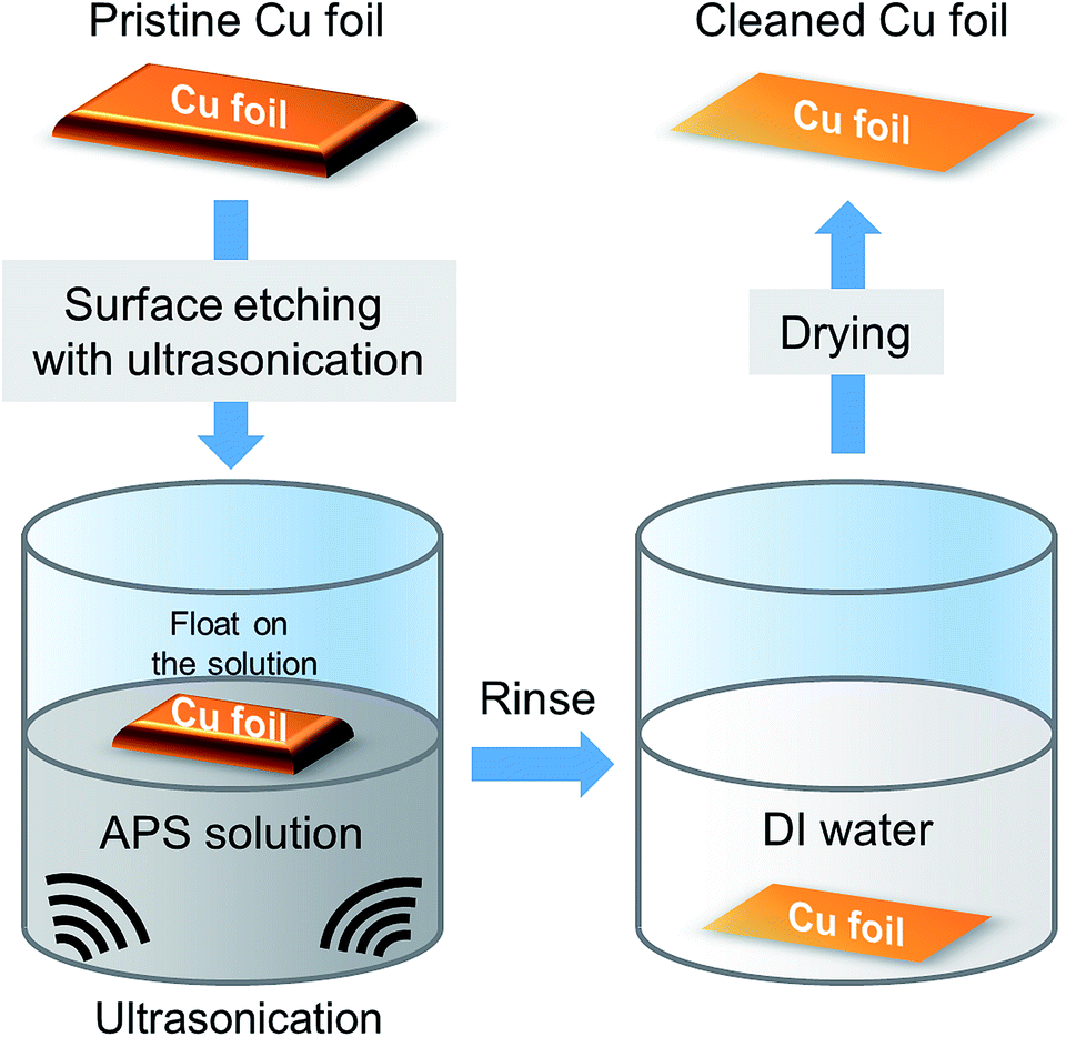 | ||
| Fig. 1 Schematic illustration of the APS solution-based precleaning method described in this study. | ||
In the meantime, a gentle ultrasonication process was applied to the solution to ensure uniform cleaning of the copper catalyst surface. During this reaction, the oxidized copper is dissolved in the solution without any harmful gaseous byproduct such as nitrogen dioxide gas. Additionally, the etching agent does not contain metallic radicals that leave metal ion residue on the cleaned copper surface, which can result in high-density nucleation of carbon during CVD growth of graphene. Here note that comparison of other copper surface engineering approaches (i.e., surface planarization/electropolishing, annealing, chemical treatment, etc.) are tabulated in Table S1.†
To elucidate the effect of the pretreatment on the copper surface morphology, Fig. 2 shows the surface characteristics of the as-received pristine and precleaned copper foils evaluated using optical microscopy (OM), scanning electron microscopy (SEM), and atomic force microscopy (AFM). As shown in Fig. 2a and c, the pristine copper foil possesses cold rolling striation lines depicted as black arrows in the images that are attributed to the typical manufacturing process for commercially available copper foil.17–19 These rolling striations are known to cause preferential graphene nucleation because of mechanical impurities such as pits or edges,18,20 and material impurities such as metal residue or intrinsic carbon contamination near the surface. As a result, they would eventually produce poor quality irregular multilayer graphene and/or carbon clusters.21,22,26 Fig. 2e and g show the surface topology image of a pristine copper catalyst substrate analyzed by AFM and a statistical histogram of the height profile, respectively. These results clearly indicate the rolling striation lines exhibit both waviness (long-range irregularities) with a maximum peak to valley distance of ∼540 nm and roughness (short-range irregularities) components. The surface characteristics of the cleaned copper catalyst substrate after conducting our pretreatment method are presented in Fig. 2b, d, f, and h. Interestingly, we could not find periodic rolling striation lines (Fig. 2b and d). Morphological analysis revealed that the cleaned copper surface exhibits increased surface roughness due to mechanical (by ultrasonication) and chemical etching of the surface, as shown in Fig. 2h. Although we did not filter out the long-range irregularities in the pristine copper substrate, the evaluated RMS value of the surface roughness of the cleaned copper substrates showed a higher value of ∼402.6 nm than that of the pristine substrate, ∼113.3 nm.
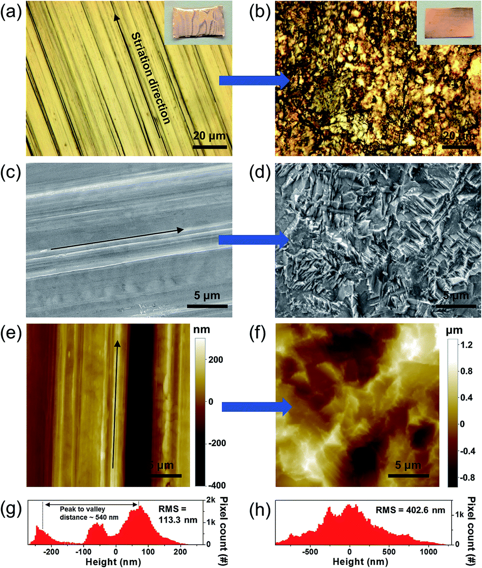 | ||
| Fig. 2 (a and b) OM, (c and d) SEM, (e and f) AFM images of the copper catalyst substrate surface for graphene growth before and after the precleaning process ((a), (c), and (e) before precleaning, (b), (d), and (f) after precleaning). The black arrows in (a), (c), and (e) represent the rolling striation direction, which is commonly observed in typical commercially available copper foils. The inset images in (a) and (b) depict photographic images of each copper substrate. Additionally, statistical histograms of the height profile of the corresponding AFM images are presented in (g) and (h) ((g) before precleaning, (h) after precleaning). | ||
To investigate the effect of the surface treatment on the quality of the synthesized graphene, we synthesized graphene thin films on both pristine and pretreated copper catalyst substrates using the CVD process. Here, we used a typical LPCVD (∼500 mTorr) process that incorporates methane gas as a precursor. First, the target copper catalyst substrates in the furnace chamber were maintained at 1050 °C for 30 min under hydrogen gas flow to remove copper oxides on the catalyst surface and facilitate surface reconstruction.14,27 Then, methane gas flowed into the chamber to provide a carbon source for graphene growth for 100 min, followed by rapid cooling of the copper foil to suppress excessive carbon atom sublimation on the surface by moving the reaction chamber away from the growth zone. Fig. 3 shows surface morphological images of both the pristine and the pretreated copper catalyst substrates after graphene growth in the CVD chamber. Here, Fig. 3a, c, and e show surface morphological images of the graphene film on the pristine copper substrate, and Fig. 3b, d, and f show images of the graphene film on the cleaned substrate obtained using OM, SEM and AFM. It was noticeable that the supersaturated carbon clusters (marked as black circles) were found only in the images of graphene films synthesized on the pristine substrate. These carbon clusters can be considered as densely nucleated carbon layers rather than bilayer graphene. According to graphene growth dynamics, the copper catalyst atoms are sublimated at the graphene growth temperature (∼1000 °C) while methane molecules are decomposed and dissolved on the copper foil surface which is dynamic equilibrium process. Thus, if the growth time is prolonged, mechanical impurities such as pits or edges on the surface of copper foil which are preferential nucleation sites for the multilayer graphene formation are reduced because of the surface reconstruction, thereby bilayer graphene could be produced.23 In the meantime, these carbon clusters originate from the rolling striations that cause preferential graphene nucleation because of metal impurities or intrinsic carbon contamination near the surface.17 Specifically, the as-received bulk copper foil usually contains localized carbon contaminants along the rolling striations in the form of structured carbon with C–C bonds. Unlike atomic carbon, which would readily diffuse in the copper surface, the structured carbon contaminants and metal impurities cannot diffuse easily on the surface.13 As a result, the localized excess carbon supersaturates the copper surface, which causes carbon clusters along the striation lines. Especially in our experiment, we could rarely observe the bilayer graphene, but the carbon clusters was found due to relatively long growth time at the growth temperature (100 min at 1050 °C with methane flow).
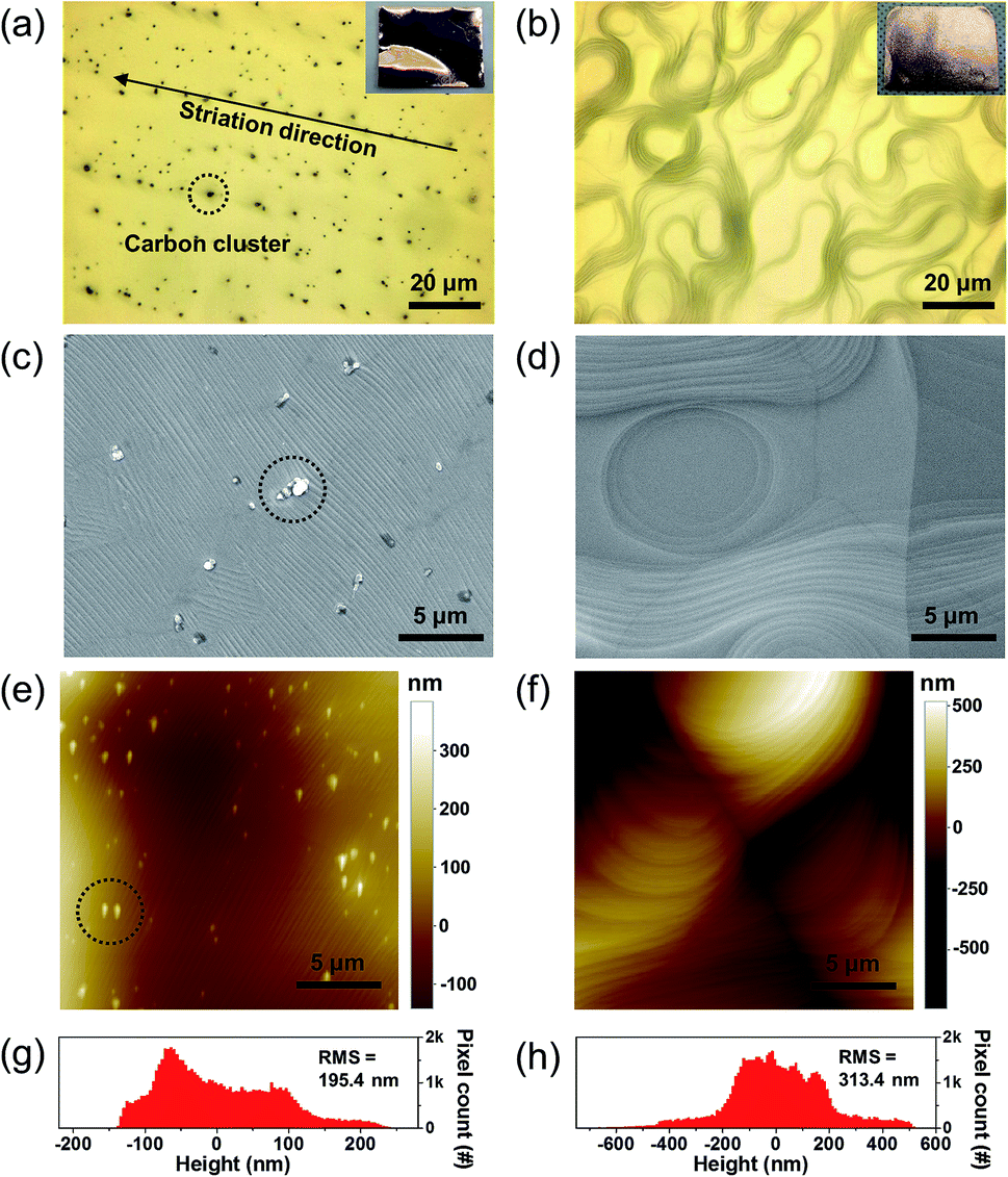 | ||
| Fig. 3 (a and b) OM, (c and d) SEM, (e and f) AFM images of the copper catalyst substrate surface after graphene growth. (a), (c), and (e) show graphene on the pristine copper substrate, while (b), (d), and (f) show graphene on the cleaned substrate. Each black dotted circle in (a), (c), and (e) represents an example of supersaturated carbon clusters on the copper substrate. The inset images in (a) and (b) depict photographic images of each copper substrate. Additionally, statistical histograms of the height profile of the corresponding AFM images are presented in (g) and (h) ((g) on the pristine copper substrate, (h) on the cleaned substrate). | ||
Meanwhile, the domain size (or nucleation density analysis) is one of the critical factors that can determine the quality of graphene. It can be investigated with the microscopic images of the graphene on a catalyst surface. Before this analysis, the nucleation density should be reduced to isolate the individual nucleation sites without covering the entire catalyst surface.24 In our experiment, however, we synthesized large-area monolayer graphene which consists of polycrystalline graphene domain covering the entire copper surface. Therefore, we could not clearly distinguish each graphene domain from Fig. 3c and d to estimate the domain size or nucleation density. Instead, from the images, we could clearly observe that there is higher wrinkle density in the graphene on the pristine copper surface as shown in Fig. S1.† Even though higher wrinkle density does not necessarily indicate the higher grain boundaries (i.e. smaller domain size and higher nucleation density), it is known that these atomic line defects such as grain boundaries in graphene can induce wrinkles on graphene.25 Therefore we might expect that the graphene grown on the pristine copper substrate contains more number of domains over the same surface area corresponding to the smaller domain size. Nevertheless, note that more rigorous analysis about the graphene domain size or nucleation density should be performed to provide a deeper insight into graphene quality.
To examine the effects of the saturated carbon clusters on the synthesized graphene film, all of the grown graphene films were transferred onto SiO2/Si substrates, as shown in Fig. 4a and b. A conventional wet transfer technique was employed that involves a PMMA sacrificial layer and wet etching of the copper catalyst substrates.28 In contrast to a flawless and uniformly continuous graphene film synthesized on the pretreated copper substrate (denoted as clean graphene), as shown in Fig. 4b, the graphene film synthesized on the pristine copper substrate (denoted as pristine graphene) shows a high density of circular etch pits with radii of several hundred nanometers (Fig. 4a). These defects attribute to the tearing of the graphene film due to striation-induced carbon clusters, which prevent the graphene film from forming a continuous layer. The surface topology image obtained by AFM indicates these etch pits more clearly, as shown in Fig. 4c. From the AFM image, it was observed that the thickness of the synthesized graphene is ∼1.0 nm, which corresponds to monolayer graphene.29 To provide a direct evidence of monolayer graphene growth, high resolution transmission electron microscopy (HRTEM) result is included in Fig. S2.† Therefore, we can expect that our pretreatment is useful for producing highly uniform graphene films, which contain negligible discontinuous defects and impurities associated with the rolling striations in a typical copper catalyst substrate. Finally, Fig. 4e depicts a schematic illustration of the generation of etch pit defects on the transferred graphene film due to the striation-induced carbon clusters along the lines. It is commonly known that the surface roughness of the copper catalyst surface can affect the quality of a synthesized graphene film. However, from our results, a more dominant determinant for improving the quality of the graphene film is the effective elimination of various impurities in the copper substrate rather than the surface roughness itself, as shown in Fig. 3g and h.26 This is mainly because even on a rough surface, faceting of the copper surface, which will facilitate high-quality monolayer graphene formation, is possible by introducing preannealing during the CVD growth process.30,31 When the copper surface is annealed at the growth temperature in the carbon-precursor-rich condition, the copper surface undergoes carbon adatoms induced faceting which produces the dense hill and valley structures on the copper surface resulting in the high surface roughness. For example, Lee et al.30 reported that they could produce better quality of graphene with the rougher copper foil because of the denser (i.e. narrower) facet structures by annealing the copper foil while flowing only methane gas prior to graphene growth. They attributed the reason that carbon adatoms can easily diffuse from one facet to another facets when their diffusion length is larger than the facet width resulting in more uniform distribution of carbon adatoms over the whole copper surface. Thus, even though the surface roughness becomes higher when the proposed pretreatment was conducted, the etched copper surface can easily facilitate narrower facet structures resulting in high-quality graphene.
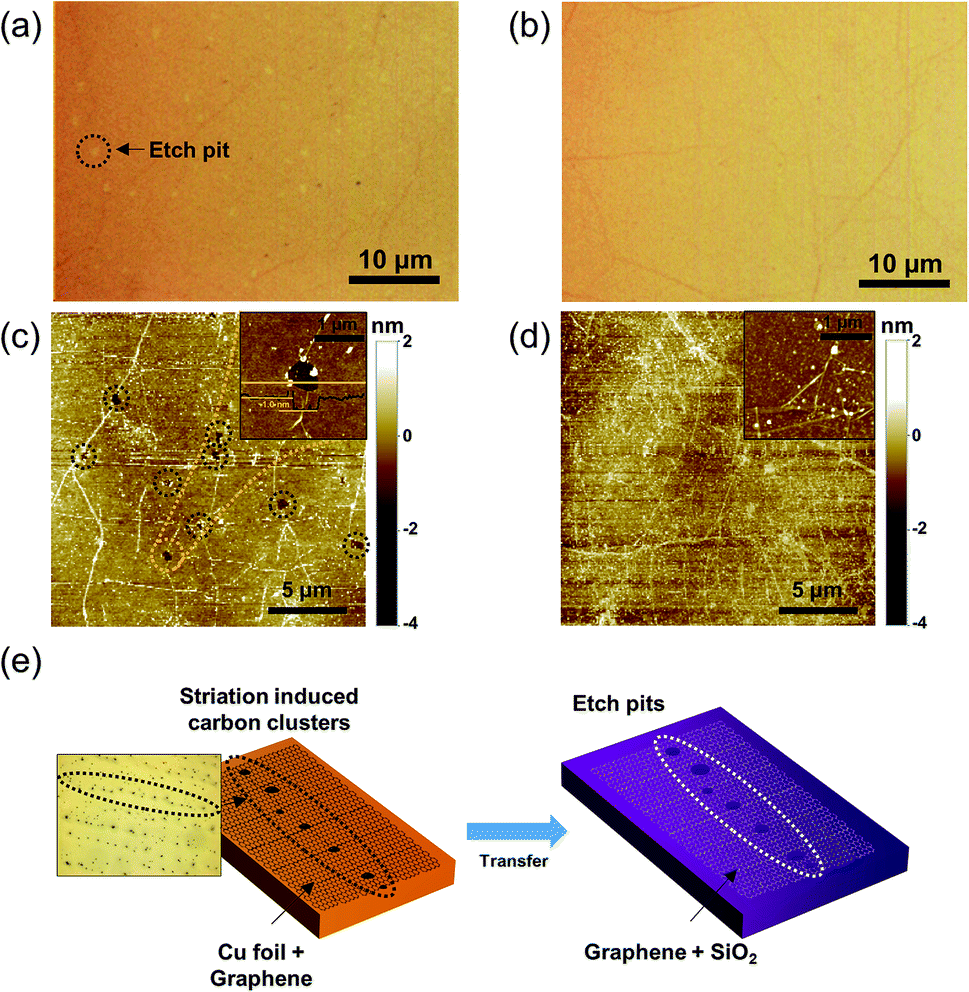 | ||
| Fig. 4 (a and b) OM, (c and d) AFM images of graphene transferred onto a SiO2/Si wafer. (a) and (c) show pristine graphene, while (b) and (d) show clean graphene. Each black dotted circle in (a) and (c) represents etch pits in the graphene film. The inset images in (b) and (d) are zoomed-in AFM images of each graphene film. From the AFM image, it is found that the thickness of the synthesized graphene is ∼1.0 nm, which corresponds to monolayer graphene. (e) Schematic illustration of the generation of etch pit defects on the transferred graphene film due to striation-induced carbon clusters along the striation lines. | ||
The quality of the graphene film transferred on SiO2/Si substrates was further evaluated with various analysis tools, such as Raman spectroscopy and sheet resistance and optical transmittance characterization. Fig. 5 depicts the Raman spectroscopy results for a transferred clean graphene film using a 532 nm laser. Graphene typically exhibits three characteristic Raman peaks with specific peak intensity ratios depending on the thickness and quality of the film.32 Fig. 5b shows three representative Raman spectra at randomly chosen positions on the graphene film transferred onto a SiO2/Si substrate marked in Fig. 5a. In Fig. 5b, two main peaks, the prominent G peak (∼1580 cm−1) and the 2D peak (∼2700 cm−1), were clearly observable from three representative Raman spectra at randomly chosen positions on the graphene transferred onto a SiO2/Si substrate. Additionally, the high intensity ratio of the 2D peak to the G peak with a negligible D peak (∼1350 cm−1) intensity, which corresponds to the defective non-sp2 domain,32 indicates high-quality synthesis of monolayer graphene on the cleaned copper substrate. For further investigation of the uniformity of the synthesized graphene film, we measured Raman mapping images on a 40 × 40 μm2 area, as shown in Fig. 5c and d. The high intensity ratio of the 2D peak to the G peak in most of the overall area in Fig. 5c indicates that clean graphene is highly homogeneous. Additionally, monolayer graphene with a small defective regions was confirmed by the low D peak to G peak intensity ratio in the area, as shown in Fig. 5d. From the statistical histogram of the intensity ratio value at each point in the area (Fig. 5e), most of the graphene region (>98%) can be considered monolayer graphene, because only <2% of the measured area exhibited a 2D peak to G peak intensity ratio below unity.32,33 This result may indicate that the thicker parts of graphene or polymer residues came from the sacrificial layer during the transfer process.33 It should be noted that these defective spots are not related to the cracks or etch pits that are depicted in Fig. 4a because the homogeneity of the films was thoroughly verified by microscopic examination before the Raman mapping showed a low D peak to G peak intensity ratio over the whole area (Fig. 5f).
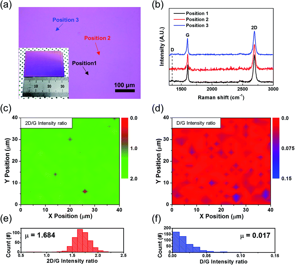 | ||
| Fig. 5 (a) OM image of the clean graphene film transferred onto a SiO2/Si substrate. Each arrow indicates three different random positions where Raman measurements are performed in (b). The inset also shows a photographic image of each copper substrate. (b) Corresponding Raman spectra of the positions in (a). (c) and (d) Raman mapping images of the graphene film: (c) 2D/G intensity ratio, (d) D/G intensity ratio. (e) and (f) Statistical histograms of the intensity ratio shown in (c) and (d): (e) 2D/G intensity ratio, (f) D/G intensity ratio. From the statistical analysis, the averaged values are found to be 1.684 and 0.017 for the 2D/G intensity ratio and D/G intensity ratio, respectively. | ||
Furthermore, we compared the electrical and optical characteristics of clean graphene and pristine graphene to investigate the quality of the films. Fig. 6a shows the sheet resistance values of the graphene films using four-point probe equipment. While pristine graphene has a larger average sheet resistance (∼427 Ω sq−1 using five different films), the cleaned copper substrate leads to a higher quality graphene film with a lower sheet resistance (∼282 Ω sq−1 using ten different films). The higher sheet resistance value of the pristine graphene is attributed to more prominent incomplete/broken regions, such as etch pits, so the charge transport ability will be degraded. In addition, optical transmittance characterization was performed to evaluate the quality of the synthesized graphene films on each copper catalyst substrate. Fig. 6b shows the optical transmittance analysis results of clean graphene and pristine graphene transferred onto quartz glass substrates. At 550 nm, the graphene films in both cases represent approximately 97.5% of the transmittance of the light, which indicates that they are predominantly monolayer graphene, considering the 2.3% expected light absorption in single-layer graphene.34 This observation is in good agreement with the Raman and AFM characterization results.
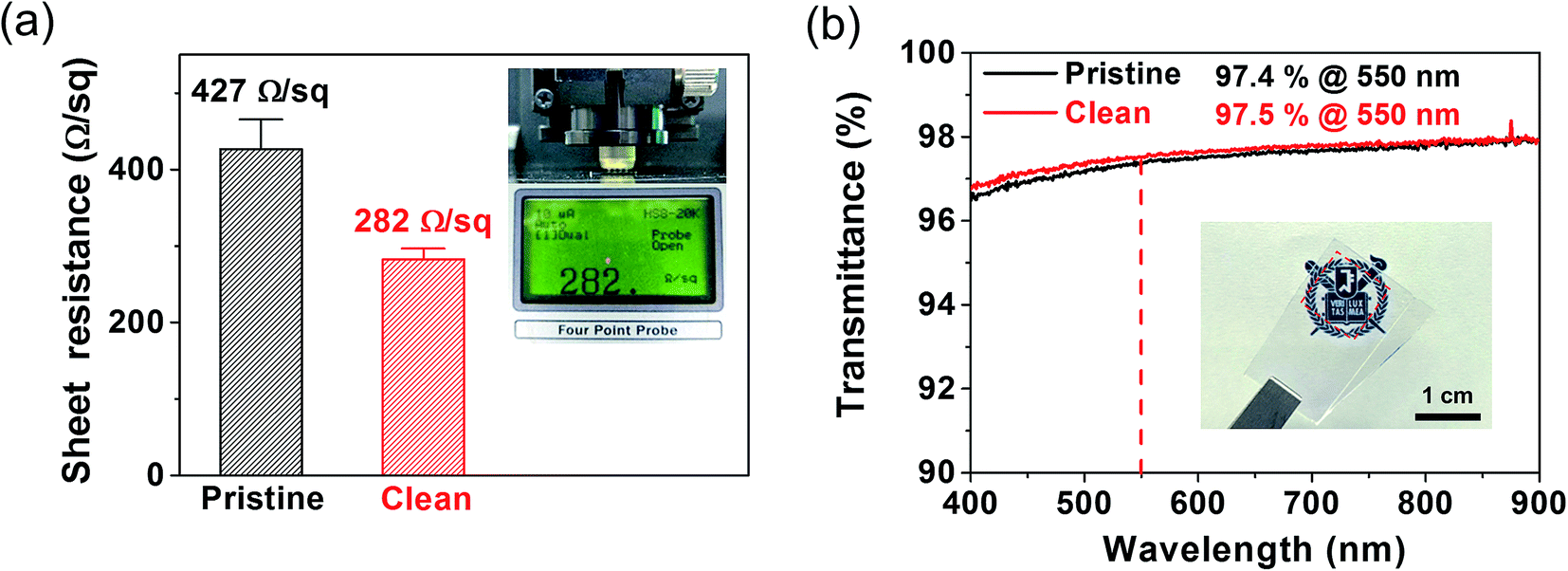 | ||
| Fig. 6 (a) Sheet resistance of the pristine graphene and clean graphene films. Inset shows the 4-probe measurement system and an example of the measured sheet resistance. (b) Optical transmittance of the pristine graphene and clean graphene films. | ||
To investigate the potential of the synthesized graphene for flexible electronic applications, the mechanical stability of our large-area synthesized graphene film was also evaluated. Fig. 7a shows a large area (40 × 40 mm2) of monolayer clean graphene that was transferred onto a flexible polyimide (PI) substrate (Neopulim L-3430). The method used to transfer the film onto the flexible substrate was the same as that mentioned in the Experimental section. The prepared pristine graphene and clean graphene maintained their electrical conductivity up to 104 cycles in a bent condition (R = 7 mm). Furthermore, graphene FETs and organic FETs (OFETs) with graphene electrodes were fabricated. As shown in Fig. 8a, the average field-effect mobility of the five different graphene FETs with the clean and pristine graphene channels were found to be ∼1066 cm2 V−1 s−1 and ∼459 cm2 V−1 s−1, respectively, calculated by μ = gmL/WCgVds, where μ is the carrier mobility, gm = dIds/dVg, L and W are the channel length and width, respectively, and Cg is the back gate capacitance. This extracted value is comparable to the previously reported results of high-quality monolayer graphene.35 Note that the Dirac voltage exhibits a p-type doped property due to the polymeric residues remaining on the surface of the transferred graphene.36–38 We also electrically characterized a pentacene OFET with graphene S/D electrodes. The transfer characteristic (S/D current versus gate voltage, Ids − Vgs) curve of the fabricated device measured at a fixed Vds of −20 V showed typical p-type FET behaviors, exhibiting an extracted field-effect mobility of ∼0.029 cm2 V−1 s−1. These results indicate that the synthesized large-area monolayer in this study is competitive to be utilized in various flexible electronic applications.
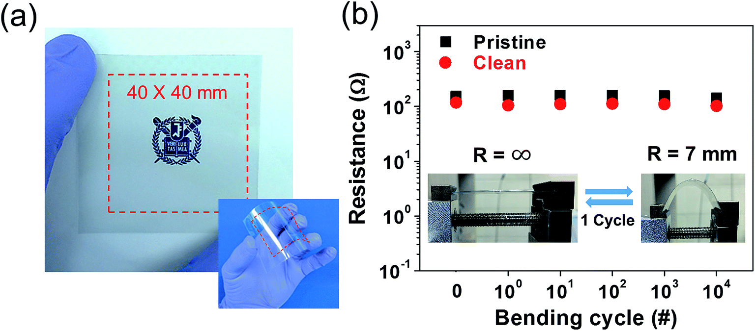 | ||
Fig. 7 (a) Photographic image of a graphene film transferred onto a flexible polyimide substrate (40 × 40 mm2). (b) The resistance of the graphene films on the flexible polyimide substrate under repeated bending cycles (0, 10, 100, 1000, and 10![[thin space (1/6-em)]](https://www.rsc.org/images/entities/char_2009.gif) 000 times; bending radius = 5 mm). 000 times; bending radius = 5 mm). | ||
 | ||
| Fig. 8 (a) Transfer characteristic curve of a graphene FET. The inset shows a photographic image of the device. (b) Transfer characteristic curve of an OFET using a graphene electrode and pentacene. | ||
4. Conclusions
In summary, we propose a new approach to introduce a pretreated surface of a copper catalyst substrate for high-quality, large-area monolayer graphene growth. Utilizing an ammonium persulfate solution and gentle ultrasonication, supersaturated striation-induced carbon clusters observed on a pristine copper catalyst substrate after graphene growth can be effectively eliminated, and thus high-quality monolayer graphene can be synthesized. This approach has attractive advantages compared to other wet copper precleaning methods using acid-based etchants: (1) no unwanted or toxic fume byproducts and (2) no metal ion residue, which will act as residual nucleation sites. The quality of clean graphene was thoroughly evaluated using Raman spectroscopy and sheet resistance, optical transmittance, and FET device characterization. The analysis results indicate that our pretreatment strategy can be beneficial for high-quality large-area synthesis of monolayer graphene that can be utilized in device applications.Conflicts of interest
There are no conflicts to declare.Acknowledgements
The authors acknowledge financial support from the National Creative Research Laboratory program (Grant No. 2012026372) through the National Research Foundation of Korea (NRF) funded by the Korean Ministry of Science and ICT. S. C. appreciates the support of the National Research Foundation of Korea (NRF) grant funded by the Ministry of Science and ICT of Korea (NRF-2017R1C1B2002323). H. J. and J. H. appreciate the financial support from the US Office of Naval Research (N000141612685) and National Science Foundation (CBET-1605338).References
- K. S. Novoselov, A. K. Geim, S. V. Morozov, D. Jiang, Y. Zhang, S. V. Dubonos, I. V. Grigorieva and A. A. Firsov, Science, 2004, 306, 666–669 CrossRef CAS PubMed.
- C. N. R. Rao, A. K. Sood, K. S. Subrahmanyam and A. Govindaraj, Angew. Chem., Int. Ed., 2009, 48, 7752–7777 CrossRef CAS PubMed.
- K. S. Kim, Y. Zhao, H. Jang, S. Y. Lee, J. M. Kim, K. S. Kim, J. H. Ahn, P. Kim, J. Y. Choi and B. H. Hong, Nature, 2009, 457, 706–710 CrossRef CAS PubMed.
- M. S. A. Bhuyan, M. N. Uddin, M. M. Islam, F. A. Bipasha and S. S. Hossain, Int. Nano Lett., 2016, 6, 65–83 CrossRef CAS.
- Z. Z. Sun, Z. Yan, J. Yao, E. Beitler, Y. Zhu and J. M. Tour, Nature, 2010, 468, 549–552 CrossRef CAS PubMed.
- S. Bae, H. Kim, Y. Lee, X. F. Xu, J. S. Park, Y. Zheng, J. Balakrishnan, T. Lei, H. R. Kim, Y. I. Song, Y. J. Kim, K. S. Kim, B. Ozyilmaz, J. H. Ahn, B. H. Hong and S. Iijima, Nat. Nanotechnol., 2010, 5, 574–578 CrossRef CAS PubMed.
- X. S. Li, W. W. Cai, L. Colombo and R. S. Ruoff, Nano Lett., 2009, 9, 4268–4272 CrossRef CAS PubMed.
- A. Cabrero-Vilatela, R. S. Weatherup, P. Braeuninger-Weimer, S. Caneva and S. Hofmann, Nanoscale, 2016, 8, 2149–2158 RSC.
- J. Seo, J. Lee, A. Jang, Y. Choi, U. Kim, H. S. Shin and H. Park, Chem. Mater., 2017, 29, 4202–4208 CrossRef CAS.
- J. Lee, J. Seo, S. Jung, K. Park and H. Park, J. Nanomater., 2018, 2018, 7610409 Search PubMed.
- Y. Zhang, L. Y. Zhang and C. W. Zhou, Acc. Chem. Res., 2013, 46, 2329–2339 CrossRef CAS PubMed.
- Q. F. Li, W. H. Liu, T. Qu, J. Zhang, X. Li, Q. K. Wang and X. L. Wang, RSC Adv., 2015, 5, 2328–2332 RSC.
- S. M. Kim, A. Hsu, Y. H. Lee, M. Dresselhaus, T. Palacios, K. K. Kim and J. Kong, Nanotechnology, 2013, 24, 365602 CrossRef PubMed.
- C. W. Magnuson, X. H. Kong, H. X. Ji, C. Tan, H. F. Li, R. Piner, C. A. Ventrice and R. S. Ruoff, J. Mater. Res., 2014, 29, 403–409 CrossRef CAS.
- G. Lupina, J. Kitzmann, I. Costina, M. Lukosius, C. Wenger, A. Wolff, S. Vaziri, M. Ostling, I. Pasternak, A. Krajewska, W. Strupinski, S. Kataria, A. Gahoi, M. C. Lemme, G. Ruhl, G. Zoth, O. Luxenhofer and W. Mehr, ACS Nano, 2015, 9, 4776–4785 CrossRef CAS PubMed.
- C. Zamfirescu, G. F. Naterer and I. Dincer, Int. J. Hydrogen Energy, 2010, 35, 4853–4860 CrossRef CAS.
- P. Braeuninger-Weimer, B. Brennan, A. J. Pollard and S. Hofmann, Chem. Mater., 2016, 28, 8905–8915 CrossRef CAS PubMed.
- A. Ibrahim, S. Akhtar, M. Atieh, R. Karnik and T. Laoui, Carbon, 2015, 94, 369–377 CrossRef CAS.
- T. J. Gnanaprakasa, Y. X. Gu, S. K. Eddy, Z. X. Han, W. J. Beck, K. Muralidharan and S. Raghavan, Microelectron. Eng., 2015, 131, 1–7 CrossRef CAS.
- S. S. Roy, N. S. Safron, M. Y. Wu and M. S. Arnold, Nanoscale, 2015, 7, 6093–6103 RSC.
- J. Kraus, M. Bobel and S. Gunther, Carbon, 2016, 96, 153–165 CrossRef CAS.
- G. Eres, M. Regmi, C. M. Rouleau, J. H. Chen, I. N. Ivanov, A. A. Puretzky and D. B. Geohegare, ACS Nano, 2014, 8, 5657–5669 CrossRef CAS PubMed.
- J. Liu, P. Li, Y. Chen, Z. Wang, J. He, H. Tian, F. Qi, B. Zheng, J. Zhou, W. Lin and W. Zhang, J. Alloys Compd., 2014, 615, 415–418 CrossRef CAS.
- C. Wang, W. Chen, C. Han, G. Wang, B. Tang, C. Tang, Y. Wang, W. Zou, W. Chen, X.-A. Zhang, S. Qin, S. Chang and L. Wang, Sci. Rep., 2014, 4, 4537 CrossRef PubMed.
- S. Deng and V. Berry, Mater. Today, 2016, 19, 197–212 CrossRef CAS.
- H. Kim, C. Mattevi, M. R. Calvo, J. C. Oberg, L. Artiglia, S. Agnoli, C. F. Hirjibehedin, M. Chhowalla and E. Saiz, ACS Nano, 2012, 6, 3614–3623 CrossRef CAS PubMed.
- Y. Jin, B. S. Hu, Z. D. Wei, Z. T. Luo, D. P. Wei, Y. Xi, Y. Zhang and Y. L. Liu, J. Mater. Chem. A, 2014, 2, 16208–16216 RSC.
- J. W. Suk, A. Kitt, C. W. Magnuson, Y. F. Hao, S. Ahmed, J. H. An, A. K. Swan, B. B. Goldberg and R. S. Ruoff, ACS Nano, 2011, 5, 6916–6924 CrossRef CAS PubMed.
- C. J. Shearer, A. D. Slattery, A. J. Stapleton, J. G. Shapter and C. T. Gibson, Nanotechnology, 2016, 27, 125704 CrossRef PubMed.
- H. C. Lee, S. B. Jo, E. Lee, M. S. Yoo, H. H. Kim, S. K. Lee, W. H. Lee and K. Cho, Adv. Mater., 2016, 28, 2010–2017 CrossRef CAS PubMed.
- T. Gao, S. B. Xie, Y. B. Gao, M. X. Liu, Y. B. Chen, Y. F. Zhang and Z. F. Liu, ACS Nano, 2011, 5, 9194–9201 CrossRef CAS PubMed.
- A. C. Ferrari and D. M. Basko, Nat. Nanotechnol., 2013, 8, 235–246 CrossRef CAS PubMed.
- E. Koo and S. Y. Ju, Carbon, 2015, 86, 318–324 CrossRef CAS.
- R. R. Nair, P. Blake, A. N. Grigorenko, K. S. Novoselov, T. J. Booth, T. Stauber, N. M. R. Peres and A. K. Geim, Science, 2008, 320, 1308 CrossRef CAS PubMed.
- C. C. Lu, Y. C. Lin, C. H. Yeh, J. C. Huang and P. W. Chiu, ACS Nano, 2012, 6, 4469–4474 CrossRef CAS PubMed.
- K. Kumar, Y. S. Kim and E. H. Yang, Carbon, 2013, 65, 35–45 CrossRef CAS.
- S. Some, J. Kim, K. Lee, A. Kulkarni, Y. Yoon, S. Lee, T. Kim and H. Lee, Adv. Mater., 2012, 24, 5481–5486 CrossRef CAS PubMed.
- A. Pirkle, J. Chan, A. Venugopal, D. Hinojos, C. W. Magnuson, S. McDonnell, L. Colombo, E. M. Vogel, R. S. Ruoff and R. M. Wallace, Appl. Phys. Lett., 2011, 99, 122108 CrossRef.
Footnotes |
| † Electronic supplementary information (ESI) available. See DOI: 10.1039/c9ra02689d |
| ‡ These authors contributed equally to this work. |
| This journal is © The Royal Society of Chemistry 2019 |