
 Open Access Article
 This Open Access Article is licensed under a Creative Commons Attribution-Non Commercial 3.0 Unported Licence
Influence of composition on the external quantum efficiency of reduced graphene oxide/carbon nanoparticle based photodetector used for human body IR detection
Mohammad Sahabul Alamab,
Monny Akter Bobyb,
Farzana Aktar Chowdhuryc,
Hamad Albrithende and
Mohammad Abul Hossain *f
*f
aDepartment of Chemical Engineering, King Abdullah Institute for Nanotechnology, King Saud University, P.O. Box 2455, Riyadh 11451, Kingdom of Saudi Arabia
bDepartment of Physics, University of Dhaka, Dhaka-1000, Bangladesh
cExperimental Physics Division, Atomic Energy Centre, 4, Kazi Nazrul Islam Avenue, Dhaka-1000, Bangladesh
dPhysics and Astronomy Department, Research Chair for Tribology, Surface and Interface Sciences, College of Science, King Abdullah Institute for Nanotechnology, Aramco Laboratory for Applied Sensing Research, King Saud University, P.O. Box 2455, Riyadh 11451, Saudi Arabia
eNational Center for Nanotechnology, King Abdulaziz City for Science and Technology, P.O. Box 6086, Riyadh 11442, Saudi Arabia
fDepartment of Chemistry, University of Dhaka, Dhaka-1000, Bangladesh. E-mail: hossainabul@yahoo.com
First published on 17th June 2019
Abstract
Here, we developed an efficient infrared (IR) detector comprising reduced graphene oxide (RGO) and carbon nanoparticles (CNPs) for detecting human body IR radiation under ambient conditions. The RGO/CNP nanocomposite thin-film based photodetectors were assembled via a simple solution-phase cost-effective route with different concentrations of RGO solution while keeping CNP concentration constant. Three RGO/CNP nanocomposite photodetector devices were fabricated with three different concentrations of RGO (keeping CNP concentration constant) and their photoresponse properties have been studied. The devices showed a sharp response to IR radiation emitted by the human body at room temperature having a wavelength of nearly 780 nm. I–V characteristics, radiation current responsivity, and time response curves as well as their external quantum efficiencies have been studied and explained. We measured two important parameters, namely, IR responsivity (Rλ) and external quantum efficiency (EQE) of RGO/CNP based IR detector devices. Our annotations show that Rλ and EQE increase with increasing concentration of GO in RGO/CNP nanocomposites as expected. This simple and inexpensive approach based on the integration of RGO and CNP could also be useful for the design of other potential optoelectronic devices such as photosensors for use in auto-doors to permit the entrance of human bodies only and in spaceships or robots to identify the existence of humans on Mars and the Moon.
1. Introduction
Graphene, a single atomic layer of two-dimensional carbon crystal, where each carbon atom is bound to another one in plane by sp2 hybridized bonds. Since the discovery of graphene, numerous research work has been performed on it.1,2 Many experimental demonstrations have revealed graphene’s extraordinary mechanical, thermal, optical, electronic and optoelectronic properties.3–5 Because of these exceptional properties, graphene is considered as a potential candidate for future generation electronic devices,6–11 energy storage devices,7,12 sensitive chemical sensors,8 biomedical applications13 including biosensing,14 bioimaging,15 thermal management,9,16 and composite materials.7,8,17 Despite having many fascinating properties, pristine graphene is not an efficient material to be used in optoelectronic devices such as photodetectors as it is a zero-bandgap semiconductor.18–20 Due to its zero-bandgap nature, the light absorption capability of graphene is very weak. It absorbs only 2.3% of light in the wide range of the visible spectrum. As a consequence, it shows very poor photoresponsivity (∼10−2 A W−1), which in fact impedes its application in optoelectronic devices.21,22 However, derivatives of graphene such as chemically converted graphene or graphene oxides (GOs) have the advantage of an open band gap and large-scale production.23 This advantage of GO has created a center of attention in science and technology as potential candidates for future applications of photocatalysts,24 ultrafiltration membranes,25,26 and optoelectronic devices such as photodetectors.27–31 The synthesized GOs are electrically insulating32–35 but these can be made conductive by annealing or chemical reduction into reduced graphene oxide (RGO),36–40 which partially recovers the physical structure of pristine graphene.Usually, the interaction of light with carbon based nanomaterials (carbon nanoparticles and graphene) results in a huge absorption of photons in the range 700–1100 nm and hence, heat is produced due to the creation of phonons owing to the strong sp2 bond in the nanostructures.41 The electronic band gap of GO can be changed over a wide range (2.2 to 0.5 eV) by altering the amount and type of oxygen-containing groups (by chemical or thermal reduction), which indicates a transition from insulator to semiconductor (usually it is called RGO).42 In most cases hydrazine is usually used for the chemical reduction of GO into RGO but its toxicity and explosiveness pose a problem.43,44 On the other hand, thermal reduction is mostly performed only at high temperatures (300–1100 °C),43–45 which is not suitable for practical applications of GO.43 Recently we reported a cost effective practical route to grow device quality RGO thin films on glass at low percolation temperature (∼200 °C) without using reagent via a simple solution casting process.43,44
Carbon-based nanomaterials such as carbon nanoparticles (CNPs) are considered as promising green materials and an alternative to traditional fluorescent nanocrystals for applications in bio-, optical, and photoacoustic imaging.46–50 Besides these, CNPs have extraordinary electrical and optical properties.51 Therefore, incorporating the outstanding optical and electrical properties of CNPs and the feasibility of RGO by the development of hybrid structures could help to make exceptional physical properties and render a potential pathway for developing high performance graphene-based material devices.
In this work, we report the influence of growth conditions on the development of RGO/CNP based human body IR radiation detectors comprising both RGO and CNP. The IR radiation emitted by the human body at room temperature has a wavelength of approximately 780 nm.52–54 Our RGO/CNP thin-film based human body IR detectors work well due to their band gap matching to the absorption at 780 nm of the photon wavelength. Such a detector will be highly applicable to identify the existence of human beings in any place such as Mars, the Moon etc.
2. Experimental
2.1. Materials
CNPs were synthesized by following the procedure reported elsewhere.51 Commercial grade diesel was collected from an oil station in Dhaka City of Bangladesh. Carbon nanomaterials were synthesized from the incomplete combustion of diesel with controlled air oxygen. At first, diesel was taken in a clean lamp and was fired. A special type of round bottom flask of glass was placed over the flame of the lamp to prevent an excess of air oxygen. During the burning of diesel, black colored materials were prepared, which were deposited inside the flask. Deposited materials were collected in a dry bottle and stored in a desiccator.GO was synthesized with Marcano’s improved method.55 Graphite flakes and KMnO4 were purchased from Alfa Aesar and Kanto Chemical, respectively. A PTFE membrane filter with a 0.45 μm pore size was purchased from Millipore. Polyester hollow fiber (Tetoron, 90 dtex, 38 mm) was purchased from Teijin Fibers. A mixture of concentrated H2SO4/H3PO4 (180 mL/20 mL; 9![[thin space (1/6-em)]](https://www.rsc.org/images/entities/char_2009.gif) :1) was added to a mixture of graphite flakes (1.5 g) and 9.0 g KMnO4. The mixture was heated with stirring at 50 °C for 14 h, which then was cooled to room temperature and poured onto ice (200 mL), which had been treated with 30% H2O2 (1.5 mL), with further cooling in an ice bath as an exothermic reaction occurred. The mixture was filtered through polyester fiber to yield dark purple solution, which was centrifuged (3750 rpm for 5–15 h), and the supernatant was decanted away. The remaining gray solid was dispersed in water (90 mL) using sonication, and filtered through the polyester fiber. The filtrate was centrifuged and the supernatant decanted away. This washing protocol (dispersion using sonication, filtration, and centrifugation) was repeated with concentrated HCl (90 mL) and ethanol (90 mL) then again with water, concentrated HCl, and ethanol. The new yellow residue was coagulated by treating it with diethyl ether, and filtered through a PTFE membrane to yield a yellow solid. The solid obtained on the filter was vacuum-dried overnight at room temperature, affording 0.4–0.6 g of dark-colored product. CNP solution in DMSO (10−7 mol L−1) was mixed with 1 mg mL−1 concentrated GO solution; and thereby, a homogeneous solution was readily obtained.
:1) was added to a mixture of graphite flakes (1.5 g) and 9.0 g KMnO4. The mixture was heated with stirring at 50 °C for 14 h, which then was cooled to room temperature and poured onto ice (200 mL), which had been treated with 30% H2O2 (1.5 mL), with further cooling in an ice bath as an exothermic reaction occurred. The mixture was filtered through polyester fiber to yield dark purple solution, which was centrifuged (3750 rpm for 5–15 h), and the supernatant was decanted away. The remaining gray solid was dispersed in water (90 mL) using sonication, and filtered through the polyester fiber. The filtrate was centrifuged and the supernatant decanted away. This washing protocol (dispersion using sonication, filtration, and centrifugation) was repeated with concentrated HCl (90 mL) and ethanol (90 mL) then again with water, concentrated HCl, and ethanol. The new yellow residue was coagulated by treating it with diethyl ether, and filtered through a PTFE membrane to yield a yellow solid. The solid obtained on the filter was vacuum-dried overnight at room temperature, affording 0.4–0.6 g of dark-colored product. CNP solution in DMSO (10−7 mol L−1) was mixed with 1 mg mL−1 concentrated GO solution; and thereby, a homogeneous solution was readily obtained.
2.2. RGO/CNP nanocomposite based device fabrication
Glass substrates were purchased from Nisshin EM Corporation, and were cleaned in an ultrasonic bath with deionized water, acetone and IPA for 15 minutes, in each case. The sample preparation was quite easy and simple. First chemically and ultrasonically cleaned glass substrate was dried with a nitrogen gas flow. After that, the glass substrate was kept in the oven. Then the GO/CNP solution was drop cast on the substrate and annealed at a temperature of 200 °C for 30 minutes to obtain the RGO/CNP film. The casting of the solution was controlled carefully due to a concern that over dropping might result in thicker films. The obtained thin film was chemically and thermally stable, homogeneous and well-adhered to the substrate as well. Table 1 presents the specifications of the three prepared RGO/CNP thin films.| Devices | Concentrations of solution | Heat treatment |
|---|---|---|
| 1 | 1.00 mg mL−1 (GO) with 10−7 mol L−1 (CNP) | 30 minutes annealing at 200 °C |
| 2 | 0.50 mg mL−1 (GO) with 10−7 mol L−1 (CNP) | 30 minutes annealing at 200 °C |
| 3 | 0.25 mg mL−1 (GO) with 10−7 mol L−1 (CNP) | 30 minutes annealing at 200 °C |
2.3. AFM measurements
In order to study the surface morphology of the GO and CNPs individually, certain amounts of low concentration GO/CNP suspension was firstly drop cast onto freshly cleaved mica substrate and spin coated (5000 rpm for 30 seconds) and heated at 100 °C for 10 minutes. After that, the samples were loaded into the microscope. Atomic force microscopy (AFM) measurements were performed using a Tapping Mode AFM (Veeco V) with an antimony doped silicon cantilever (model: TESPA). Mica substrates were purchased from Nisshin EM Corporation. Resolution for topography measurements was 512512 points at 1 Hz frequency. Fig. 1(a, b) and 2 were produced using the program WSxM.56
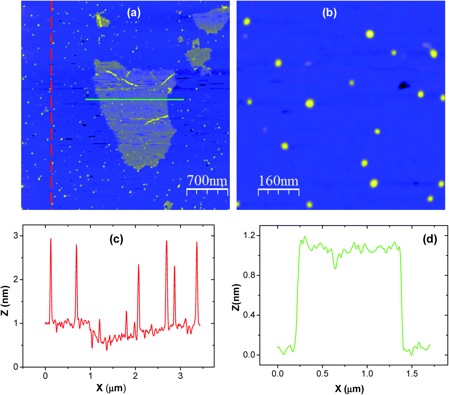 | ||
| Fig. 1 (a) An AFM image of exfoliated GO and CNPs deposited on mica substrate. (b) A magnified AFM image of isolated CNPs deposited on a mica substrate, (c) a 2D line profile recorded along the red dotted line on the CNP dots in (a), and (d) a 2D line profile recorded along the green line on the graphene sheet in (a). | ||
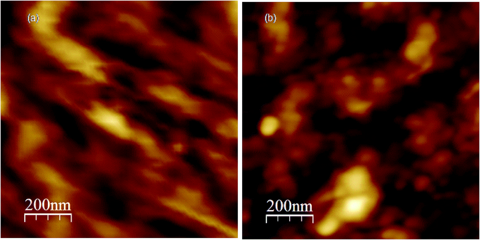 | ||
| Fig. 2 (a) An AFM topography image of GO film on glass substrate of concentration 1 mg mL−1, (b) an AFM topography image of RGO/CNP nanocomposite (device-1). | ||
2.4. Optical measurements
The transmittance of the films was studied using a spectroscopic Ellipsometer (WVAZE, J. A. Woollam inc) capable of measuring the transmittance of polarized light. In that system, the incident angle of the light on the samples surface was 0°. The system has a wide range spectrum in the range 300–2500 nm. The absolute intensity of the transmitted beam was divided by the source intensity without a sample to extract the transmittance (T).2.5. IR response study
The room temperature DC transport measurements were carried out using a standard two-probe technique. A ‘Keithley’ 2401 source meter unit was used for current measurements as a function of time (at 2 V power supply) under radiation emitted by a human body. Two indium electrodes were fabricated on RGO/CNP thin films at approximately 2 mm distance. Body current was measured with time by holding one hand in close proximity to the film at different distances from the device.3. Results and discussion
In order to show the achievement of single-sheet GO and individual CNPs, a droplet of low concentration GO/CNP suspension was dropped onto the mica substrate for AFM measurements. Fig. 1(a) shows an AFM image of single GO flakes as well as isolated CNPs. A magnified AFM image of Fig. 1(a) is presented in Fig. 1(b), where isolated CNPs of different sizes are clearly visible. A 2D line profile was recorded along the red dashed line in Fig. 1(a) and presented in Fig. 1(c), which shows that the size distribution of isolated CNPs varies from 1 to 3 nm. Another 2D profile was recorded along the green solid line in Fig. 1(a) and presented in Fig. 1(d). The profile indicates that the thickness of the GO sheet is approximately 1 nm, which roughly confirms the detection of a single GO sheet.Fig. 2(a) shows an AFM topography image of GO thin film used in this study. The average thickness of the film obtained by AFM measurement is 35.2 nm and the surface root mean square (RMS) roughness is 2.79 nm. It is noteworthy that the film thickness exceeds the thickness of a single layer of graphene oxide of ∼1 nm, demonstrating that the prepared film consists of multiple layers of GO. Fig. 2(b) shows the AFM surface morphology of one of the RGO/CNP based IR detector devices (device-1). The image shows homogeneous deposition of the RGO/CNP nanocomposite on the glass surface. These measurements show a simple synthetic strategy for anchoring single-nanoparticle systems on RGO.54 The average thicknesses are 27.5 and 22.3 nm and the corresponding RMS roughness are 1.48 and 1.25 nm measured directly by AFM for the device-2 and device-3, respectively.
Fig. 3 demonstrates the optical transmittance spectra for all three samples in the photon wavelength range between 300 and 2500 nm. The RGO/CNP nanocomposite films show roughly horizontal transmittances of photon wavelength regime starting from 2500 down to 1750 nm for sample-1 (device-1), 2500 down to 1200 nm for sample-2 (device-2), and 2500 down to 750 nm for sample-3 (device-3), showing transmittances from 82 to 90%. At around 800, 700, and 500 nm a sharp absorption takes place for sample-1, sample-2, and sample-3, respectively, where transmittance reaches approximately down to zero. The absorption of light at 800 nm for sample-1 approximately corresponds to the wavelength of IR radiation emitted by the human body at room temperature. This indicates that sample-1 has a band gap which lies close to the IR radiation of wavelength 780 nm emitted by the human body at room temperature, making it an interesting candidate for application in IR sensing devices.
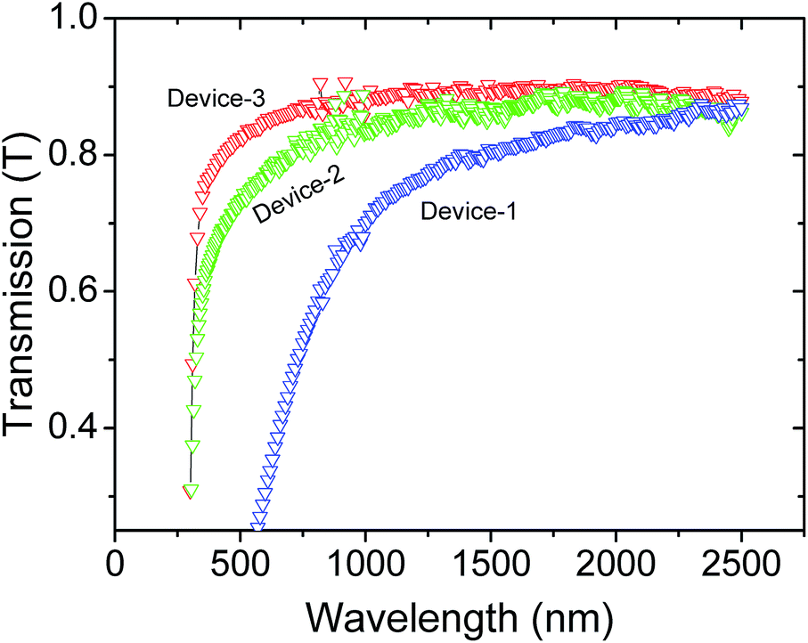 | ||
| Fig. 3 Optical transmittance as a function of photon wavelength for three different RGO/CNP devices. Concentrations of GO were 1 mg mL−1, 0.5 mg mL−1 and 0.25 mg mL−1 for device 1, 2, and 3, respectively. Concentration of CNP was kept constant in all cases, which was 10−7 mol L−1. | ||
A schematic diagram of an IR detector device for electrical measurement is shown in Fig. 4(a). The current–voltage characteristics of the IR detector devices with and without IR irradiation are shown in Fig. 4(b) and (c). Dark current (ID) and the current due to human body IR radiation (Iλ) were measured at room temperature where the Iλ current data was measured after 5 minutes of continuous human body radiation exposure. The current (Iλ) was calculated by subtracting the dark current (ID) from the irradiation current [Iλ = Iirradiation − ID]. In all irradiation current measurements, a hand was used as an IR source.
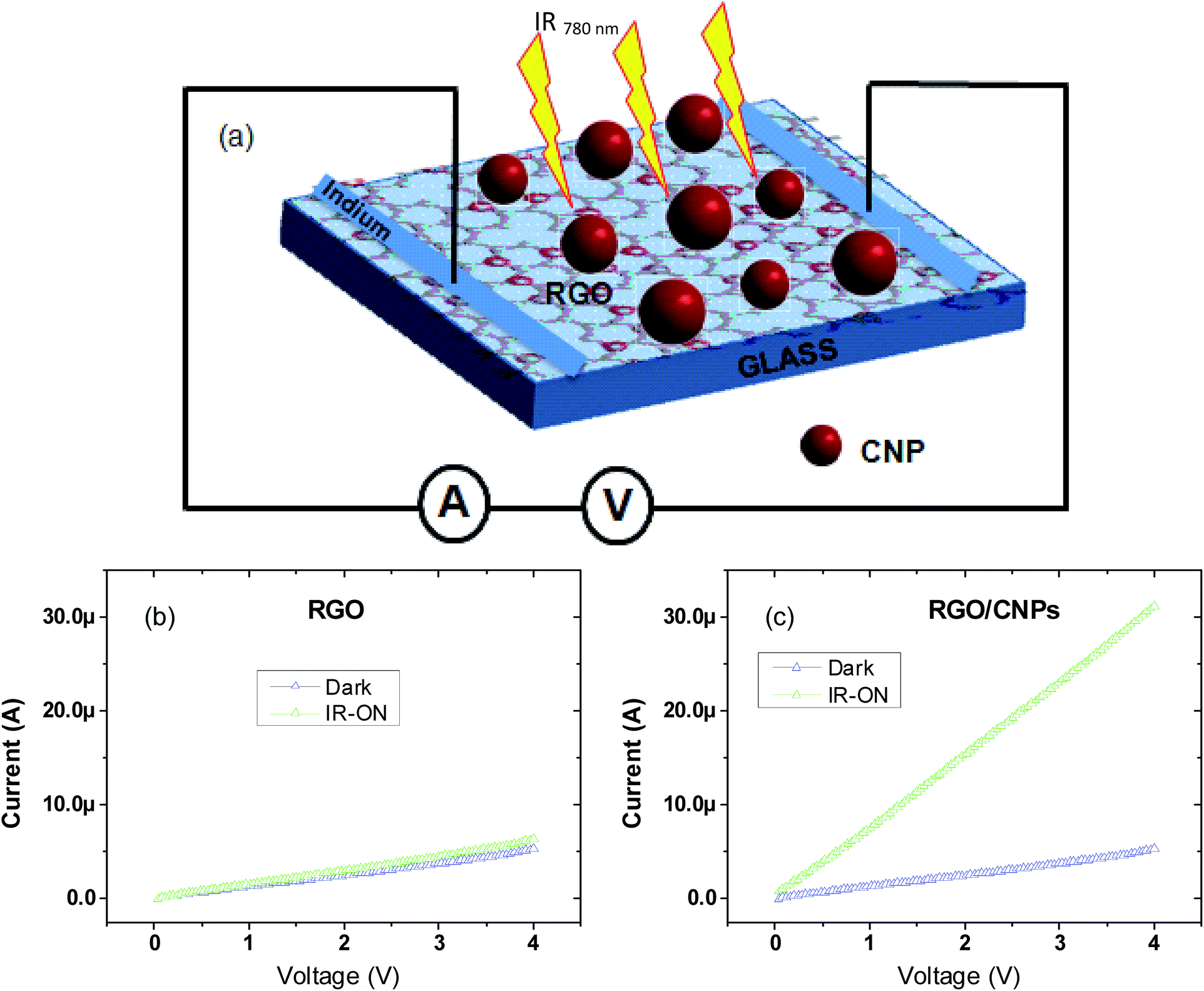 | ||
| Fig. 4 (a) A schematic illustration of the device configuration for IR response studies, (b) I–V characteristics curve with and without IR irradiation of one of the RGO based IR detector devices and (c) one of the RGO/CNP nanocomposite based IR detector devices. | ||
In order to explore the electrical contact between RGO and CNPs in the nanocomposite, the I–V properties (Fig. 4(c)) of one of the fabricated devices were measured (device-1) under IR radiation emitted by the human body. As a control experiment we also measured I–V properties (Fig. 4(b)) of a RGO based IR detector. Fig. 4(b) shows that there is no significant current change on IR irradiation by the hand, demonstrating a very low IR response in the RGO film. However, a linear I–V curve (representing the ohmic contact) was obtained with the same IR irradiation for the RGO/CNP nanocomposite device (device-1), indicating that there is a strong interaction between RGO and CNPs in the nanocomposite (Fig. 4(c)). The current also increases on IR irradiation of the RGO/CNP based nanocomposite. In the above cases, the source of IR radiation (hand) was kept 2 cm away from the device at room temperature. The starting value of the sweep voltage was 0 volts and the stop voltage was 4 volts. From the above graph (Fig. 4(c)), we see that the radiation current rises significantly when the source (hand) of IR radiation was brought into a close vicinity of the detector. It is seen from Fig. 4(c) that the current due to radiation is approximately 5 times higher than the dark current.
We also investigated time-resolved IR response for three different devices under radiation from a human hand at a bias voltage of 2 V. When the hand is placed in the proximity of the device (IR at ON state), current starts rising immediately and reaches the saturation value. The RGO/CNP nanocomposite based detector shows good response under IR radiation from a hand and this phenomenon continued repeatedly and is presented for 3 cycles in Fig. 5(a). It demonstrates persistent IR response with less deviation. When the hand is put away from the device (IR is at OFF state), the current promptly recuperates to its initial value. It means the radiation-current retention time (RRT) is very poor. The RRT is defined as the time a radiation current can be sustained in the sample after the IR is switched OFF. The rise and fall of the current due to a hand in repeated proximity and removal (12 cycles) is presented in Fig. 5(b). The device demonstrates excellent cyclability, which is a key feature for measuring the permanence of the device under prolonged application.57
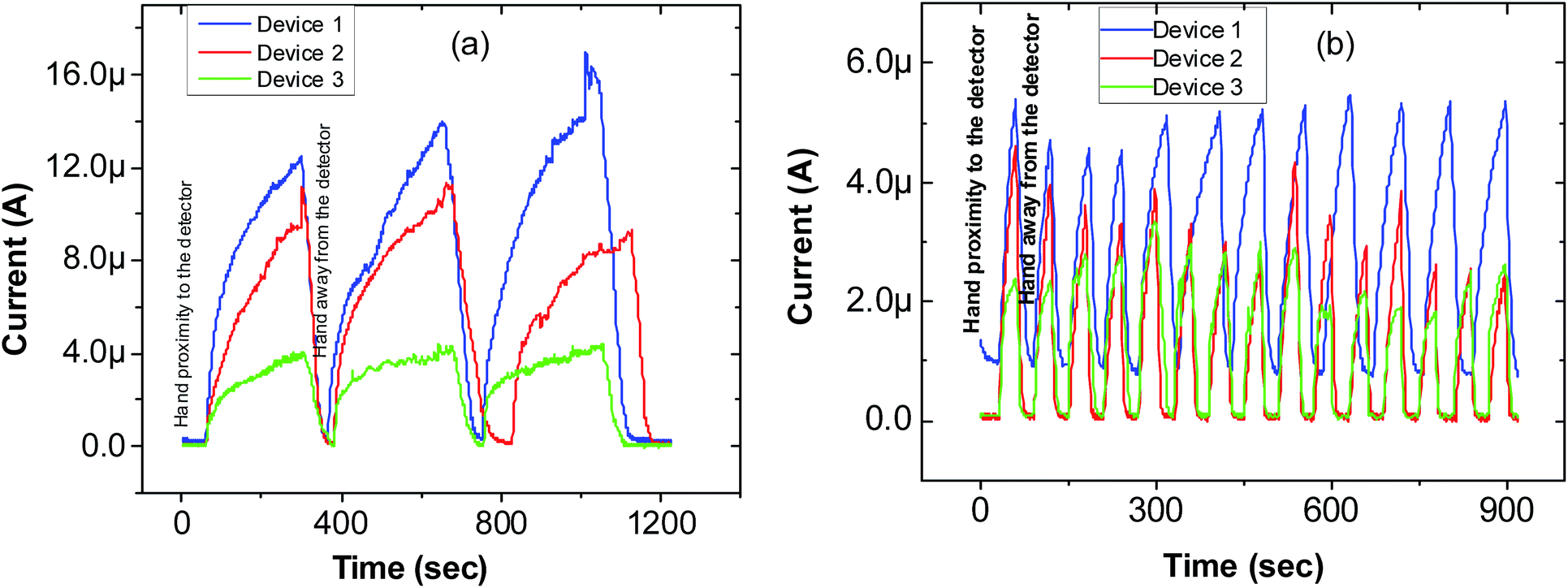 | ||
| Fig. 5 (a) Time-dependent IR response study of the RGO/CNP nanocomposite under radiation due to a hand, (b) rapid growth and decay of the current due to a hand in repeated proximity and removal for device-1 (blue), device-2 (red), and device-3 (green). | ||
The continuous current rising was detected under IR radiation due to a hand by the three different devices as a function of time and plotted in Fig. 6(a). It is seen from Fig. 6(a) that the rise of the current persists for quite a long time of about 10 minutes. After that, it goes to a saturated regime. The growth curve consists of faster and slower parts. These effects are due to transient current and capacitive effects. These two effects can be calculated by fitting the growth curve with an exponential function and working out for the time constants.57 The growth of current due to IR radiation by hand as a function of time fits well with the eqn (1) of exponential growth:
| It = I0 + C(1 − exp(−t/τC)) + D(1 − exp(−t/τD)) | (1) |
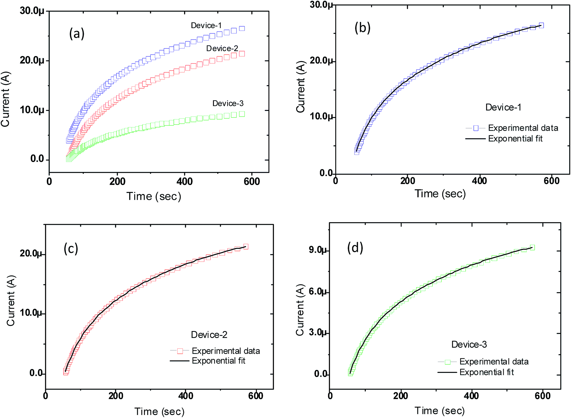 | ||
| Fig. 6 (a) Exponential rise of current with time for device-1, device-2, and device-3 respectively; (b–d) exponential fit to the experimental data points presented in (a). In all cases, the source of radiation (hand) was kept at a distance of about 2 cm away above the detector. | ||
We also observed in Fig. 6(a) that the higher the concentration of graphene oxide is, the higher the current under IR irradiation is. The increase of current with increasing concentration of graphene oxide matched with the expected outcome. The higher is the concentration of the GO materials in the solution, the higher the thickness of the RGO/CNP based devices/films. The higher current is related to the band gap (or thickness of the films) of the composite materials. The band gap of the RGO/CNP nanocomposite is inversely proportional to the square of the RGO/CNP film thickness (Eg ∼ 1/d2).60–62 The quantum size effect could be a probable reason for the change in the band gap with varying thickness of RGO/CNP thin films. This can be elucidated in the following way. The thin RGO/CNP films (nanoscale range) are considered as one-dimensional confined or low-dimensional systems or quantum-dimensional structures (quantum well) where electron motion is limited in one direction (for example Z-direction or the thickness direction) and electrons can move freely (infinite or unlimited motion) in the other two directions (for example X- and Y-direction). The size of this quantum-mechanical object or quantum well is comparable to the electron de Broglie wavelength.62 In such a quantum-well, the electronic properties are usually different from those of bulk materials and hence low-dimensional effects become perceptible. In this low-dimensional system, the quantum-mechanical laws direct different processes and the energy spectrum, which describes the electron motion in the confined region, becomes discrete and thus the band gap of a semiconductor becomes size dependent.62
For one-dimensional materials, quantum confinement of electron motion increases the electron minimum energy. In the case of nanometer length, the distance between two energy levels increases when the size of the film thickness (i.e. the confinement direction thickness) decreases, as described by ΔEg ≈ (h2/2md2),60–62 where d is the thickness of the layer and m is the effective mass of an electron. This equation can usually elucidate the band gap increase with decreasing film thickness (or vice versa) in the nanometer scale range.60–62
The variation of radiation current as a function of distance between source and detector were also studied. Fig. 7(a) shows the variation of current for the three devices as function of distance. The radiation current decreases with increasing distance (Fig. 7(a)). During this work, the source of radiation (hand) was kept at distances of 2, 3, 4, and 5 cm away from the detector. The linear fit to the experimental data points for three devices of Fig. 7(a) are presented in Fig. 7(b–d), respectively. We observed that the value of current strongly depends on the concentration of GO solution as well as the distance between the source of radiation and the detector.
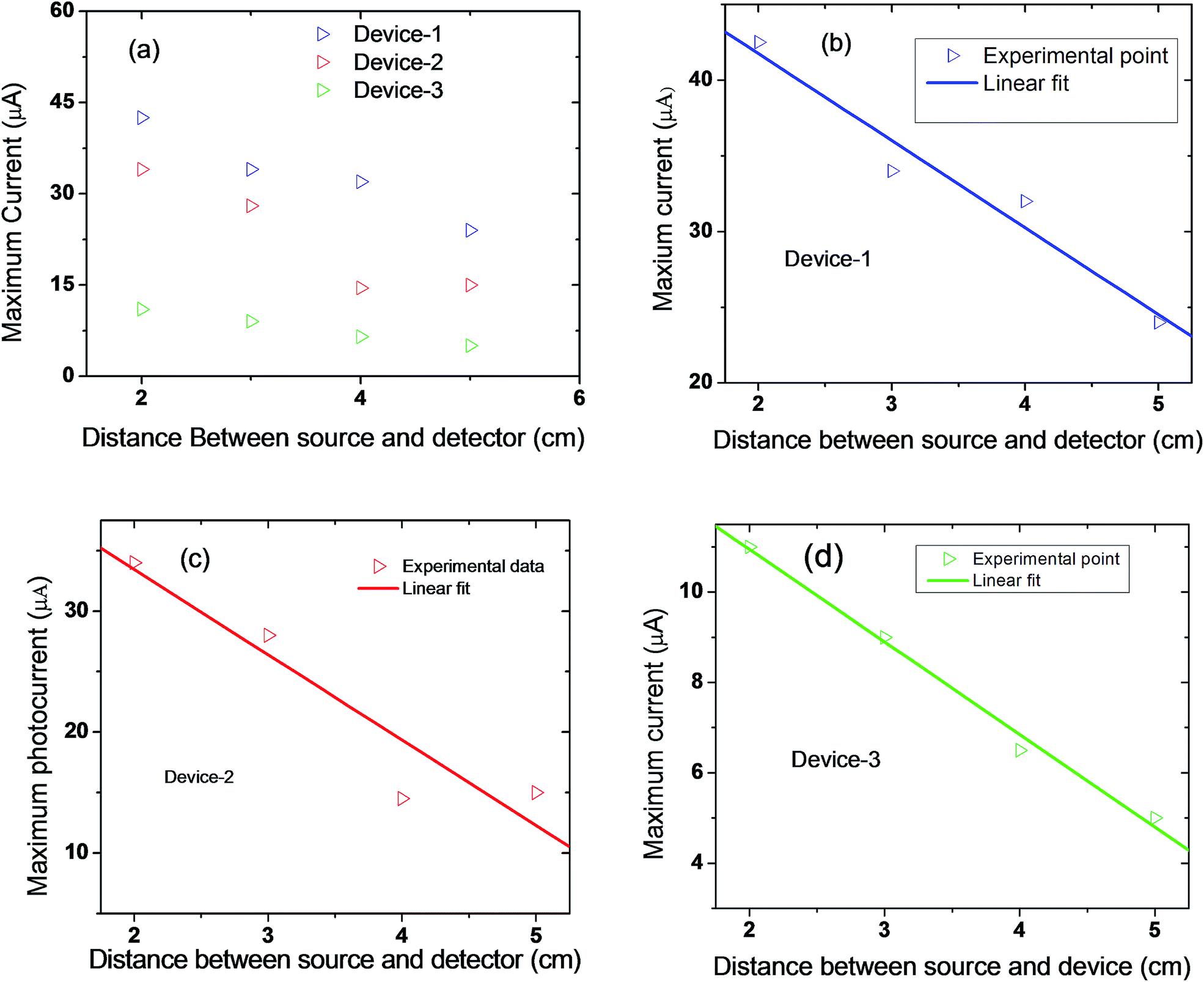 | ||
| Fig. 7 (a) Variation of maximum IR current with distance for three devices; (b–d) linear fit to the experimental data points presented in (a). | ||
The GO concentration dependent EQE of the devices is shown in Fig. 8. It should be mentioned here that the concentration of nanoparticle was kept constant for all devices at 10−7 mol L−1. We observed that the EQE increases linearly with increasing concentration of GO in the solution as expected.
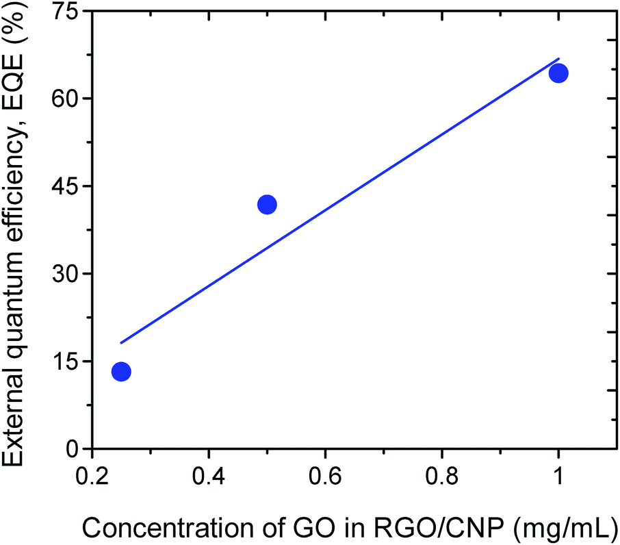 | ||
| Fig. 8 EQE vs. concentration of GO in the solution of the detector devices. | ||
Two important parameters, radiation-responsivity (Rλ) and external quantum efficiency (EQE), were calculated to demonstrate its detection efficiency. The Rλ is defined as the ratio of output current to the incident energy of IR radiation on the effective area of a detector,63 whereas the EQE is another factor which measures the quality of performance of a radiation-detecting device and is defined as the number of electrons perceived per incident photon. The two parameters, Rλ and EQE, can be assessed by using eqn (2) and (3).63,64
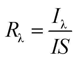 | (2) |
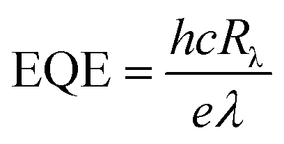 | (3) |
| Devices | Rλ (A W−1) | EQE (%) |
|---|---|---|
| Device-1 | 0.40 | 64.32 |
| Device-2 | 0.26 | 41.81 |
| Device-3 | 0.08 | 13.22 |
We calculated two important parameters, Rλ and EQE, for all three devices and found 0.40, 0.26, and 0.08 A W−1 and 64.32%, 41.81%, and 13.22%, respectively. The acquired data were very much reproducible for all devices with no degradation of the device performance. Our fabricated devices have band gaps which lie very close to the IR radiation emitted by the human body (∼780 nm) at room temperature, which is why they did not respond to other sources with wavelengths other than 780 nm. The working principle of RGO/CNP devices under IR irradiation can be explained by the principle of photon excitation. Under IR irradiation on devices, the number of photons absorbed or dissipated by the RGO/CNP thin film provides the subsequent number of photoelectrons. The incident photon energy can be calculated by the eqn (4)
| E = hc/λ | (4) |
4. Conclusion
The synthesis of RGO/CNP nanocomposites and their IR response properties are reported. The GO was synthesized by Hummers’ modified method and CNPs were synthesized from diesel. The structural and morphological information of the sample properties were studied using AFM. In this work, three devices were fabricated with three different concentrations of GO, where CNP concentration was kept constant at 10−7 mol L−1. The current responsivity of the GO detectors was found to be 0.40 A W−1, 0.26 A W−1 and 0.08 A W−1, respectively, whereas external quantum efficiencies of 64.32%, 41.81%, and 13.22% were obtained for the devices 1, 2 and 3, respectively, for an incident IR wavelength of 780 nm emitted by the human body. Recently, Chowdhury et al. have reported IR response of 3 mA W−1 and an external quantum efficiency of 0.48% for an IR detector made-up using a GO/CNP composite [AIP Advances].54 Here we report that the RGO/CNP nanocomposite based IR detectors show improved performance in terms of IR responsivity and external quantum efficiency as compared to the reported GO/CNP based IR detector.54 All these results evidently demonstrate that the RGO/CNP nanocomposite could be one of the primary potential materials for sensing IR radiation emitted by human body.Conflicts of interest
There are no conflicts to declare.Acknowledgements
The authors are grateful to the University of Dhaka, Bangladesh and King Saud University, Kingdom of Saudi Arabia for the opportunity to perform the research work. This research was financially supported by the International Science Programme (ISP), Sweden.References
- K. S. Novoselov, A. K. Geim, S. V. Morozov, D. Jiang, Y. Zhang, S. V. Dubonos, I. V. Grigorieva and A. A. Firsov, Science, 2004, 306, 666 CrossRef CAS PubMed.
- A. K. Geim and K. S. Novoselov, Nat. Mater., 2007, 6(3), 183 CrossRef CAS PubMed.
- K. S. Novoselov, A. K. Geim, S. V. Morozov, D. Jiang, M. I. Katsnelson, I. V. Grogorieva, S. V. Dubonos and A. A. Firsov, Nature, 2005, 438, 197 CrossRef CAS PubMed.
- K. S. Novoselov, Z. Jiang, Y. Zhang, S. V. Morozov, H. L. Stormer, U. Zeitler, J. C. Maan, G. S. Boebinger, P. Kim and A. K. Geim, Science, 2007, 315, 1379 CrossRef CAS PubMed.
- N. Tombros, C. Jozsa, M. Popinciuc, H. T. Jonkman and B. J. van Wees, Nature, 2007, 448, 571 CrossRef CAS PubMed.
- H. Chang and H. Wu, Adv. Funct. Mater., 2013, 23(16), 1984 CrossRef CAS.
- Y. An, A. Behnam, E. Pop, G. Bosman and A. Ural, J. Appl. Phys., 2015, 118(11), 114307 CrossRef.
- M. Zhu, X. Li, S. Chung, L. Zhao, X. Li, X. Zang and H. Zhu, Carbon, 2015, 84, 138 CrossRef CAS.
- Y. Lee, S. H. Yu, J. Jeon, H. Kim, J. Y. Lee, H. Kim and J. H. Cho, Carbon, 2015, 88, 165 CrossRef CAS.
- S. H. Cheng, T. M. Weng, M. L. Lu, W. C. Tan, J. Y. Chen and Y. F. Chen, Sci. Rep., 2013, 3, 2694 CrossRef PubMed.
- Y. Kim, S. J. Kim, S. P. Cho, B. H. Hong and D. J. Jang, Sci. Rep., 2015, 5, 12345 CrossRef CAS PubMed.
- W. Jiang, H. Wang, Z. Xu, N. Li, C. Chen, C. Li, J. Li, H. Lv, L. Kuang and X. Tian, Chem. Eng. J., 2018, 335, 954 CrossRef CAS.
- P. Zhao, Q. Xu, J. Tao, Z. Jin, Y. Pan, C. Yu and Z. Yu, Wiley Interdiscip. Rev.: Nanomed. Nanobiotechnol., 2017, 10(3), e1483 Search PubMed.
- Y. Yang, W. Xuefeng, L. Guochao, X. Liu, Q. Chen, H. Li, L. Lu, P. Zhao and Z. Yu, J. Colloid Interface Sci., 2017, 509, 515 CrossRef PubMed.
- Y. Yang, Q. Chen, S. Li, W. Ma, G. Yao, F. Ren, Z. Cai, P. Zhao, G. Liao, J. Xiong and Z. Yu, J. Biomed. Nanotechnol., 2018, 14(8), 1396 CrossRef CAS PubMed.
- Z. Zhao, K. Teng, N. Li, X. Li, Z. Xu, L. Chen, J. Niu, H. Fu, L. Zhao and Y. Liu, Composite Structures, 2017, 159, 761 CrossRef.
- S. Stankovich, D. A. Dikin, G. H. Dommett, K. M. Kohlhaas, E. J. Zimney, E. A. Stach, R. D. Piner, P. S. Nguyen and R. S. Ruoff, Nature, 2006, 442, 282 CrossRef CAS PubMed.
- E. J. H. Lee, K. Balasubramanian, R. T. Weitz, M. Burghard and K. Kern, Nat. Nanotechnol., 2008, 3, 486 CrossRef CAS PubMed.
- S. C. B. Mannsfeld, et al., Nat. Mater., 2010, 9, 859 CrossRef CAS PubMed.
- H. Chang, Z. Sun, M. Saito, Q. Yuan, H. Zhang, J. Li, Z. Wang, T. Fujita, F. Ding, Z. Zheng, F. Yan, H. Wu, M. Chen and Y. Ikuhara, ACS Nano, 2013, 7, 6310 CrossRef CAS PubMed.
- T. Van Tam, S. H. Hur, J. S. Chung and W. M. Choi, Sens. Actuators, A, 2015, 233, 368 CrossRef.
- Y. Zhang, T. Liu, B. Meng, X. Li, G. Liang, X. Hu and Q. J. Wang, Nat. Commun., 2013, 4, 1811 CrossRef PubMed.
- H. Tian, H. Y. Chen, T. L. Ren, C. Li, Q. T. Xue, M. A. Mohammad, C. Wu, Y. Yang and H. S. P. Wong, Nano Lett., 2014, 14(6), 3214 CrossRef CAS PubMed.
- Z. Xu, T. Wu and J. Shi, J. Membr. Sci., 2018, 520, 281 CrossRef.
- J. Zhang, Z. Xu, M. Shan, B. Zhou, Y. Li, B. Li, J. Niu and X. Qian, J. Membr. Sci., 2013, 448, 81 CrossRef CAS.
- H. Kang, W. Wang, J. Shi, Z. Xu, H. Lv, X. Qian, L. Liu, M. Jing, F. Li and J. Niu, Appl. Surf. Sci., 2019, 465, 1103 CrossRef CAS.
- C. Metzger, E. Fleisch, J. Meyer, M. Dansachmüller, I. Graz, M. Kaltenbrunner, C. Keplinger, R. Schwödiauer and S. Bauer, Appl. Phys. Lett., 2008, 92, 013506 CrossRef.
- B. Tian, et al., Science, 2010, 329, 830 CrossRef CAS PubMed.
- F. A. Chowdhury, T. Mochida, J. Otsuki and M. S. Alam, Chem. Phys. Lett., 2014, 593, 198 CrossRef CAS.
- S. C. Dhanabalan, J. S. Ponraj, Q. Bao and H. Zhang, Nanoscale, 2016, 8(12), 1 RSC.
- F. Jones, et al., Adv. Mater., 2017, 29, 1702993–1702997 CrossRef.
- M. Acik, G. Lee, C. Mattevi, M. Chhowalla, K. Cho and Y. J. Chabal, Nat. Mater., 2010, 9(10), 840 CrossRef CAS PubMed.
- G. Eda and M. Chhowalla, Adv. Mater., 2010, 22(22), 2392 CrossRef CAS PubMed.
- F. Jabbarzadeh, M. Siahsar, M. Dolatyari, G. Rostami and A. Rostami, Appl. Phys. B, 2015, 120(4), 637 CrossRef CAS.
- H. Chang, Z. Sun, Q. Yuan, F. Ding, X. Tao, F. Yan and Z. Zheng, Adv. Mater., 2010, 22(43), 4872 CrossRef CAS PubMed.
- M. Acik, G. Lee, C. Mattevi, M. Chhowalla, K. Cho and Y. J. Chabal, Nat. Mater., 2010, 9(10), 840 CrossRef CAS PubMed.
- K. P. Loh, O. Bao, G. Eda and M. Chhowalla, Nat. Chem., 2010, 2(12), 1015 CrossRef CAS PubMed.
- Z. Liu, K. Parvez, R. Li, R. Dong, X. Feng and K. Müllen, Adv. Mater., 2015, 27(4), 669 CrossRef CAS PubMed.
- Y. Lee, S. H. Yu, J. Jeon, H. Kim, J. Y. Lee, H. Kim, J. H. Ahn, E. Hwang and J. H. Cho, Carbon, 2015, 88, 165 CrossRef CAS.
- M. Zhu, X. Li, Y. Guo, X. Li, P. Sun, X. Zang, K. Wang, M. Zhong, D. Wu and H. Zhu, Nanoscale, 2014, 6(9), 4909 RSC.
- Q. Zeng, S. Wang, L. Yang, Z. Wang, T. Pei, Z. Zhang, L. M. Peng, W. Zhou, J. Liu, W. Zhou and S. Xie, Opt. Mater. Express, 2012, 2(6), 839 CrossRef CAS.
- H. Shi, C. Wang, Z. Sun, Y. Zhou, K. Jin, S. A. T. Redfern and G. Yang, Opt. Express, 2014, 22(16), 19375 CrossRef PubMed.
- F. A. Chowdhury, T. Morisaki, J. Otsuki and M. S. Alam, Appl. Surf. Sci., 2012, 259, 460 CrossRef CAS.
- F. A. Chowdhury, T. Mochida, J. Otsuki and M. S. Alam, Chem. Phys. Lett., 2014, 593, 198 CrossRef CAS.
- Q. He, H. G. Sudibya, Z. Yin, S. Wu, H. Li, F. Boey, W. Huang, P. Chen and H. Zhang, ACS Nano, 2010, 4(6), 3201 CrossRef CAS PubMed.
- J. Zhu, A. Holmen and D. Chen, ChemCatChem, 2013, 5, 378 CrossRef CAS.
- S. K. Bhunia, N. Pradhan and N. R. Jana, ACS Appl. Mater. Interfaces, 2014, 6, 7672 CrossRef CAS.
- S. T. Yang, L. Cao, P. G. J. Luo, F. S. Lu, X. Wang, H. F. Wang, M. J. Meziani, Y. F. Liu, G. Qi and Y. P. Sun, J. Am. Chem. Soc., 2009, 131, 11308 CrossRef CAS PubMed.
- L. Wu, X. Cai, K. Nelson, W. Xing, J. Xia, R. Zhang, A. J. Stacy, M. Luderer, G. M. Lanza, L. V. Wang, B. Shen and D. Pan, Nano Res., 2013, 6, 312 CrossRef CAS PubMed.
- S. C. Ray, A. Saha, N. R. Jana and R. Sarkar, J. Phys. Chem. C, 2009, 113, 18546 CrossRef CAS.
- M. A. Hossain, S. Islam, F. A. Chowdhury, K. Uchida, T. Tamura, K. Sugawa, T. Mochida, J. Otsuki, T. G. Mohiuddin and M. S. Alam, Fullerenes, Nanotubes, Carbon Nanostruct., 2015, 24, 43 CrossRef.
- J. C. Joshi and A. L. Dawar, Phys. Status Solidi A, 1982, 70(2), 353 CrossRef CAS.
- M. Shankar, J. B. Burchett, Q. Hao, B. D. Guenther and D. J. Brady, Opt. Eng., 2006, 45(10), 106401 CrossRef.
- F. A. Chowdhury, M. A. Hossain, K. Uchida, T. Tamura, K. Sugawa, T. Mochida, J. Otsuki, T. Mohiuddin, M. A. Boby and M. S. Alam, AIP Adv., 2015, 5(10), 107228 CrossRef.
- D. C. Marcano, D. V. Kosynkin, J. M. Berlin, A. Sinitskii, Z. Sun, A. Slesarev, L. B. Alemany, W. Lu and J. M. Tour, ACS Nano, 2010, 4, 4806 CrossRef CAS PubMed.
- I. Horcas, R. Fernández, J. M. Gómez-Rodríguez, J. Colchero, J. Gómez-Herrero and A. M. Baro, Rev. Sci. Instrum., 2007, 78, 013705 CrossRef CAS.
- S. Ratha, A. J. Simbeck, D. J. Late, S. K. Nayak and C. S. Rout, Appl. Phys. Lett., 2014, 105(24), 243502 CrossRef.
- B. Chitara, L. S. Panchakarla, S. B. Krupanidhi and C. N. R. Rao, Adv. Mater., 2011, 23, 5419 CrossRef CAS PubMed.
- S. Ghosh, B. K. Sarker, A. Chunder, L. Zhai and S. I. Khondaker, Appl. Phys. Lett., 2010, 96, 163109 CrossRef.
- E. S. Goh, T. P. Chen, C. Q. Sun and Y. C. Liu, J. Appl. Phys., 2010, 107(2), 024305 CrossRef.
- M. Fox, Optical Properties of Solids, Oxford University Press, Oxford, 2001 Search PubMed.
- V. Mitin, D. Sementsov and N. Vagidov, Chapter One, Quantum Mechanics for Nanostructures, Cambridge University Press, 2010 Search PubMed.
- H. Morkoç, A. D. Carlo and R. Cingolani, Solid-State Electron., 2002, 46, 157 CrossRef.
- J. P. Cheng, Y. J. Zhang and R. Y. Guo, J. Cryst. Growth, 2008, 310, 57 CrossRef CAS.
- T. Ueda, A. H. An, K. Hirakawa and S. Komiyama, J. Appl. Phys., 2008, 103, 093109 CrossRef.
- X. P. Chen, H. L. Zhu, J. F. Cai and Z. Y. Wu, J. Appl. Phys., 2007, 102, 024505 CrossRef.
| This journal is © The Royal Society of Chemistry 2019 |