
 Open Access Article
 This Open Access Article is licensed under a Creative Commons Attribution-Non Commercial 3.0 Unported Licence
Strain engineering of optical activity in phosphorene
Doan Quoc Khoaab,
Masoumeh Davoudiniyac,
Bui Dinh Hoi*d and
Mohsen Yarmohammadi *c
*c
aDivision of Computational Physics, Institute for Computational Science, Ton Duc Thang University, Ho Chi Minh City, Viet Nam. E-mail: doanquockhoa@tdtu.edu.vn
bFaculty of Electrical and Electronics Engineering, Ton Duc Thang University, Ho Chi Minh City, Viet Nam
cDepartment of Energy Engineering and Physics, Amirkabir University of Technology, Tehran, Iran. E-mail: davoudiniya.m@aut.ac.ir; my69@aut.ac.ir
dDepartment of Physics, University of Education, Hue University, Hue City, Viet Nam. E-mail: buidinhhoi@hueuni.edu.vn
First published on 17th June 2019
Abstract
Optical activity is one of the most fascinating fields in current physics. The strong anisotropic feature in monolayer phosphorene leads to the emergence of non-trivial optoelectronic physics. This paper is devoted to a detailed analysis of strain effects on the optical activity of phosphorene ranging from low-optical-field to high-optical-field. To do so, a numerical study of the two-band tight-binding model is accomplished using the Harrison rule and the linear response theory. Although the transparency of phosphorene confirms at all frequencies independent of the strain modulus and direction, on average, from low- to high-optical-field limit, the polarization of the reflected wave at critical strains becomes circular and the ellipse axis tends to a rotation of 180°. It is found that the maximum absorption takes place at high-energy transitions, which quantitatively depends strongly on the strain modulus and direction. Furthermore, a detailed investigation of compressive and tensile strains results in the dominant contribution of the in-plane compressive and out-of-plane tensile strains to the reflected/transmitted light for low- and intermediate-optical-field ranges, whilst both contribute for the high-optical-field limit. However, overall, in-plane compressive and out-of-plane tensile strains come in to play a role in the absorption spectra. Thereby, the quality of the determined reflection, transmission and absorption waves depends on the regarded regime of the optical field, strain modulus, and strain orientation. These findings if sufficient can be performed and/or tuned experimentally, and a vast number of phosphorene-based optoelectronic devices can be achieved.
1 Introduction
In contrast to graphene and other two-dimensional (2D) materials,1–8 monolayer black phosphorus, phosphorene, has emerged as a promising candidate for widespread applications.9,10 Phosphorene’s high ON/OFF ratio and carrier mobility overcome the limitations of field effect transistors based on other 2D materials in industry,11–14 such as the low ON/OFF ratio in graphene and low carrier mobility in transition-metal dichalcogenides. These two important properties have recently attracted a lot of attention in condensed matter physics and material science.15–17 Phosphorene is a 2D direct-gap (⋍1.5 eV) semiconductor with a side view non-planar puckered structure, but a top view similar to graphene, which can be produced experimentally using mechanical exfoliation methods.11–14,16A vast number of experimental and theoretical works have endeavoured to achieve new physical insights from black phosphorus, including the fields of optical,16,18–20 thermal,21–23 electrical,17,24–26 and mechanical physics.27 For instance, different phases for black phosphorus have been obtained using density functional theory (DFT) by applying a perpendicular electric field and in-plane strain.28,29 In other studies, it has been shown that the puckered structure of phosphorene makes it more flexible in practice. This, in turn, sustains it in the presence of elastic deformations as large as 30%.30,31 Strain engineering is one of the well-known strategies to make phosphorene an encouraging material for possible applications because strain affects the bond length between the nearest and the next-nearest atoms and eventually the in-plane and out-of-plane nearest-neighbor hopping. In ref. 19, 32 and 33, the variation of the band gap of phosphorene as a function of strain modulus was obtained analytically, showing that monolayer phosphorene is more stable under tensile strains than compressive ones. In very recent work, the possible uni-, bi-, and tri-axial strain-induced electronic phase transitions in phosphorene have been investigated using the density of states quantity through the Harrison relation.34 Their findings report that the electronic phase of phosphorene can be adjustable in the presence of strain.
Phosphorene is also notable for its remarkable anisotropic properties. In general, phosphorene possesses orientation-dependent carrier effective masses and carrier velocities, in contrast to other 2D systems.17,18,20,24,35 This feature distinguishes phosphorene from other 2D materials and leads to unparalleled physical properties. For example, it has been reported that there is a red shift (blue shift) in the optical transitions under compressive (tensile) strain.36 And it has been found that phosphorene absorbs less light energy polarized along the armchair direction than along the zigzag direction, resulting in maximized optical conductivity in the armchair direction.19 These studies provide high feasibility for the applications of phosphorene-based optoelectronic devices. The strain engineering of phosphorene leads to the potential application for it as a photocatalyst as well. Not only in our theoretical results, but also in ref. 37, they have unraveled strain engineered phosphorene as a photocatalyst in the application of water splitting hydrogen production based on DFT calculations.
In this paper, we will be concentrated on the effects induced by applied uniaxial strain on the interband optical activity of phosphorene. Although the optical conductivity as a function of frequency ω and the strain modulus ε has been studied well in ref. 38, the optical activity of strained phosphorene is still an open issue and, to the best of our knowledge, has not been theoretically well addressed yet. To do so, the uniaxial strain is applied in a tight-binding model Hamiltonian using the Harrison rule and the optical activity is derived within the linear response theory. Our results confirm that strain has a significant effect on the optical activity of phosphorene.
The paper is organized as follows. In Sections 2 and 3 we review the tight-binding model for pristine and strained phosphorene and discuss the formation of the band gap with respect to strain modulus and direction. In Section 4 we derive the optical activity quantities of phosphorene. In Section 5 we present the main results and summarize our conclusions in Section 6.
2 Two-band pristine Hamiltonian model of phosphorene
In this section, we first concentrate on the atomic configuration of phosphorus atoms in monolayer phosphorene comprising two sublayers, for which each sublayer consists of two atoms in a unit cell. The characteristic structure of such a system is sketched in Fig. 1. This configuration demands a model to describe the carrier dynamics. In so doing, we use the tight-binding approximation.20,35,39 This leads to the following Hamiltonian in real-space
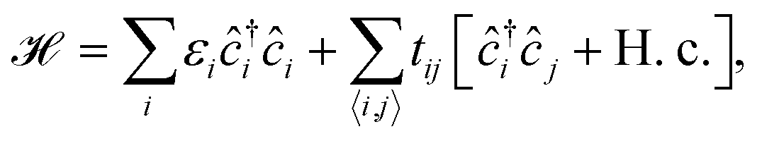 | (1) |
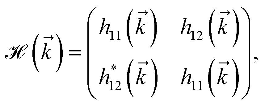
![[k with combining right harpoon above (vector)]](https://www.rsc.org/images/entities/i_char_006b_20d1.gif) = (kx,ky) as20
= (kx,ky) as20
 | (2) |
h11() = 4t4![[thin space (1/6-em)]](https://www.rsc.org/images/entities/char_2009.gif) cos(kxa/2)cos(kyb/2), cos(kxa/2)cos(kyb/2),
| (3a) |
|
h12() = 2t1e−ikxa1xcos(kyb/2) + t2eikxa2x + 2t3eikxa3xcos(kyb/2) + t5e−ikxa5x.
| (3b) |
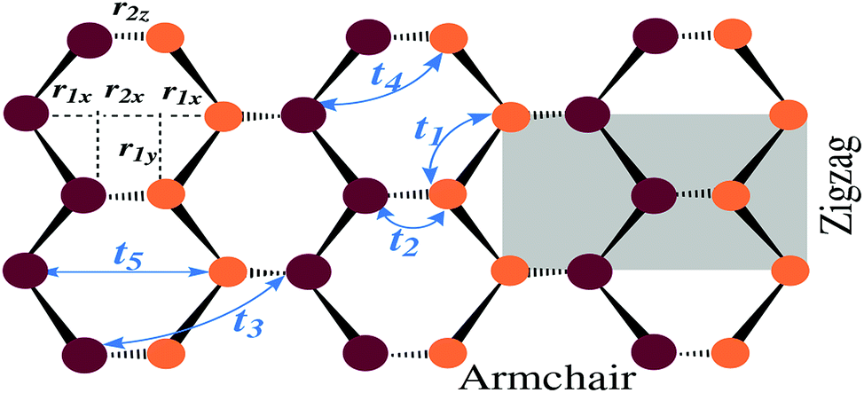 | ||
| Fig. 1 Schematic diagram of the top view of monolayer black phosphorene structure. The upper (lower) sublayer is shown by the crimson (orange) circles. t{1,2,3,4,5} are the hopping energies corresponding to five nearest neighbor lattice sites. The unit cell of monolayer phosphorene consisting of four phosphorus atoms is shown by a shadowed rectangle. Also, r1{x,y} and r2x stand for the projection of phosphorus atoms in the same and different sublayers, respectively, while r2z = 2.14 Å is the thickness of monolayer phosphorene. | ||
Given that the unit cell of monolayer phosphorene contains four atoms, the symmetry property between atoms in two different sublayers leads to the 2 × 2 Hamiltonian matrix above, where clearly there is no term for the on-site energies inside the structure factors. The parameters a1x = 1.41763 Å, a2x = 2.16400 Å, a3x = 3.01227 Å, a4x = 2.21468 Å, and a5x = 3.63258 Å20,35,38 are the distance between the intra- and inter-planar nearest-neighbor atoms projected to the armchair (x) direction.
In order to calculate the dispersion energy of carriers in phosphorene, one needs to diagonalize the Hamiltonian in eqn (2), leading to
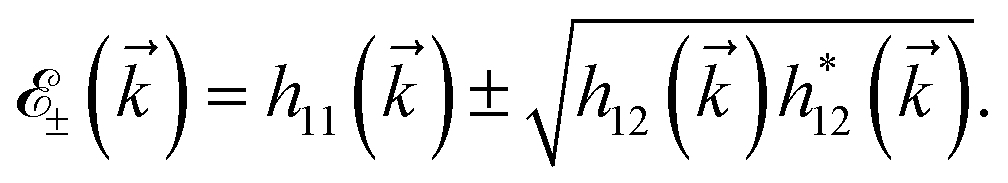 | (4) |
3 Two-band strained Hamiltonian model of phosphorene
The pristine model can be extended to the strained model, however, one needs the modified hopping energies because by applying strain the bond lengths, the bond angles and eventually the hopping integral energies between lattice sites alter.33,42 From ref. 32, the tight-binding model is adequate to consider the strain effects on phosphorene. In the presence of strain, the initial coordinates of atomic site i ∈ {1, 2} [see Fig. 1] are deformed to new coordinates as
 | (5) |
![[r with combining right harpoon above (vector)]](https://www.rsc.org/images/entities/i_char_0072_20d1.gif) iβ and
iβ and  are the strain modulus, the initial coordinates before applying strain and final coordinates after applying strain, respectively, along the β-direction for β = {x, y, z}. Accordingly, the norm of
 ![[r with combining tilde]](https://www.rsc.org/images/entities/i_char_0072_0303.gif) i in the linear deformation regime can be connected to the norm of ri via
i in the linear deformation regime can be connected to the norm of ri via  where the dimensionless geometrical coefficients αβi = (iβ/ri)2 can be taken from ref. 32, 39 and 43, (0.4460, 0.5571, 0), (0.0992, 0, 0.9052), (0.7505, 0.2461, 0), (0.3976, 0.2280, 0.3722), and (0.7530, 0, 0.2538), corresponding to the hopping energy t1, t2, t3, t4, and t5, respectively.
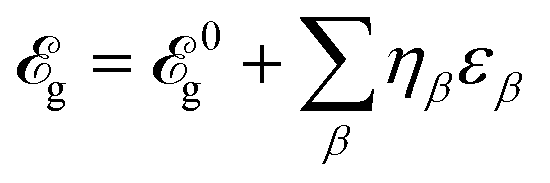
So far, we obtained the deformed coordinates in real-space, however, the linear deformation regime above-mentioned can be written for the hopping energies as well using the relation [ti ∝ ri−2],44,45 leading to
 | (6) |
![[t with combining tilde]](https://www.rsc.org/images/entities/i_char_0074_0303.gif) i. Thereby, the two-band strained Hamiltonian model of phosphorene is similar to eqn (2) and (3) but by replacing ti → i. It is necessary to mention that the dispersion energy relation of carriers in strained phosphorene is exactly the same as eqn (4) but with strained structure factors. For this reason, we would like to rename them
i. Thereby, the two-band strained Hamiltonian model of phosphorene is similar to eqn (2) and (3) but by replacing ti → i. It is necessary to mention that the dispersion energy relation of carriers in strained phosphorene is exactly the same as eqn (4) but with strained structure factors. For this reason, we would like to rename them  . Note that we label the tensile and compressive strains with the sign + and −, respectively, throughout the paper.
Fig. 2(a) depicts the electronic band structure plot of pristine monolayer phosphorene along the high symmetry points X ← Γ → Y of the first Brillouin zone (FBZ) of phosphorene [see the inside rectangle of Fig. 2(a)]. First of all, our two-band model confirms the high anisotropic property of phosphorene stemming from the carrier Fermi velocities and effective masses along the different edges.20 Second, the bands show that the band gap of about  is located at the Γ point. Since there is no further information around the S point of the FBZ at all, in what follows we will only focus on the X–Γ–Y region in order to apply the uniaxial strains and in order to study the strained optical activities.
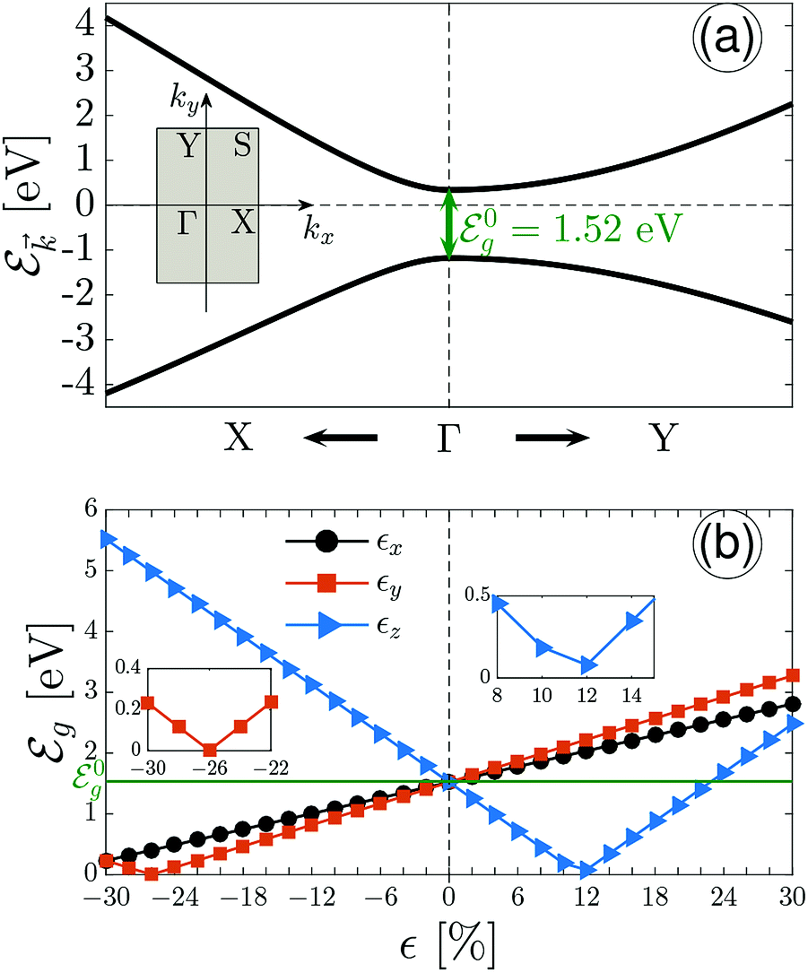 | ||
Fig. 2 (a) The electronic band structure of pristine monolayer phosphorene with the fixed Fermi energy at  . The band gap is about 1.52 eV. The inset shadowed rectangle stands for the FBZ of phosphorene. (b) The electronic band gap as a function of strain. . The band gap is about 1.52 eV. The inset shadowed rectangle stands for the FBZ of phosphorene. (b) The electronic band gap as a function of strain. | ||
Although the investigation of the band’s behavior with uniaxial strain might be interesting, however, we only plot the band gap as a function of strain (both compressive and tensile) along the x, y and z direction in Fig. 2(b). In order to have a stable lattice structure after applying strain, we restrict ourselves to the strains up to 30% along each direction for both compressive and tensile cases. We have chosen this limit because, as mentioned before, in DFT calculations,30,31 it has been shown that the structure of monolayer phosphorene on average is stable under a critical strain up to 27% and 30% along the zigzag and armchair direction, respectively. One may observe that the band gap increases with strain along the x direction linearly, while interestingly, different behaviors are seen for the y and z directions. The band gap decreases with compressive strain from −30% to −26% and surprisingly gets zero value at εy = −26%, however, it increases with both cases after this critical strain modulus. This critical strain refers to the semiconductor-to-metal transition point. As for the z direction, one may distinguish among results compared to the other two directions. For compressive strains, the band gap decreases completely, while it decreases with tensile strains up to εz = +12% and increases after this point. This point can be referred to as the semiconductor-to-semimetal transition point.
In short, the various possible electronic phases can be grouped into three families, according to the band gap treatment: (1) semiconductor in the presence of uniaxial strain along the x direction independent of the compressive and/or tensile case, (2) semiconductor-to-metal phase transition at εy = −26% in the presence of uniaxial strain along the y direction and (3) semiconductor-to-semimetal phase transition at εz = +12% in the presence of uniaxial strain along the z direction. Note that the transition between two different phases takes place when the band gap line touches or approaches the strain axis. The results reported here are consistent with the theoretically observed critical points.38,46,47 Although uniaxial strain is included in a standard model Hamiltonian at the tight-binding level, this might not nonetheless be exactly the same result as DFT and experiments observe. It is worth deriving the border between the energy gap and the strain modulus (for both εβ < 0 and εβ > 0) as
 | (7) |
4 Optical activity of strained phosphorene
In this section, we intend to calculate the responses of strained monolayer phosphorene when an electromagnetic wave propagates through it. This is known as the optical activity feature including data about the reflected, transmitted and absorbed waves. On the other hand, in our formulation, these data rely on the assumption that the interband optical conductivity responds to applied strain so that the effect of strain on the propagation of an electromagnetic wave can be studied straightforwardly. To achieve this purpose, let the complex two-component electric fields![[E with combining right harpoon above (vector)]](https://www.rsc.org/images/entities/i_char_0045_20d1.gif) i, r =
i, r = ![[r with combining circumflex]](https://www.rsc.org/images/entities/i_char_0072_0302.gif) i, t =
i, t = ![[t with combining circumflex]](https://www.rsc.org/images/entities/i_char_0074_0302.gif) i at z = 0 be the incident, reflected and transmitted parts of the electromagnetic wave, respectively. One has the reflection and transmission matrices. Note that in our formulation both the incident and scattered plane waves are perpendicular to the phosphorene.
i at z = 0 be the incident, reflected and transmitted parts of the electromagnetic wave, respectively. One has the reflection and transmission matrices. Note that in our formulation both the incident and scattered plane waves are perpendicular to the phosphorene.
Since the incident, reflected and transmitted parts of the electromagnetic wave with and without applied strain are supposed to be connected by the boundary conditions 1 = 2 and −i![[small tau, Greek, circumflex]](https://www.rsc.org/images/entities/i_char_e0b8.gif) y(
y(![[H with combining right harpoon above (vector)]](https://www.rsc.org/images/entities/i_char_0048_20d1.gif) 1 − 2) = 4π
1 − 2) = 4π![[small sigma, Greek, circumflex]](https://www.rsc.org/images/entities/i_char_e111.gif) /c [1(2) denotes the top (bottom) surface of phosphorene], we can safely work for the low enough thickness of phosphorene where refers to the magnetic field part of the incident wave and c is the velocity of light.52–54 As usual, y is the y component of the Pauli matrices and stands for the interband optical conductivity tensor. It is useful to only subject the top surface of phosphorene to the incident wave, for which the electric fields can be defined as 1 = i + r and 2 = t, and the magnetic fields for the vacuum at each side are defined by the relation = ẑ × . Thus, the matrix forms of the reflection and transmission coefficients are given by
/c [1(2) denotes the top (bottom) surface of phosphorene], we can safely work for the low enough thickness of phosphorene where refers to the magnetic field part of the incident wave and c is the velocity of light.52–54 As usual, y is the y component of the Pauli matrices and stands for the interband optical conductivity tensor. It is useful to only subject the top surface of phosphorene to the incident wave, for which the electric fields can be defined as 1 = i + r and 2 = t, and the magnetic fields for the vacuum at each side are defined by the relation = ẑ × . Thus, the matrix forms of the reflection and transmission coefficients are given by
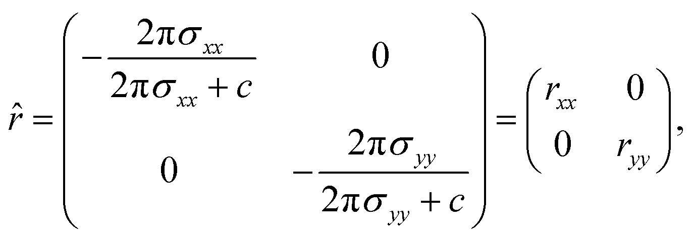 | (8a) |
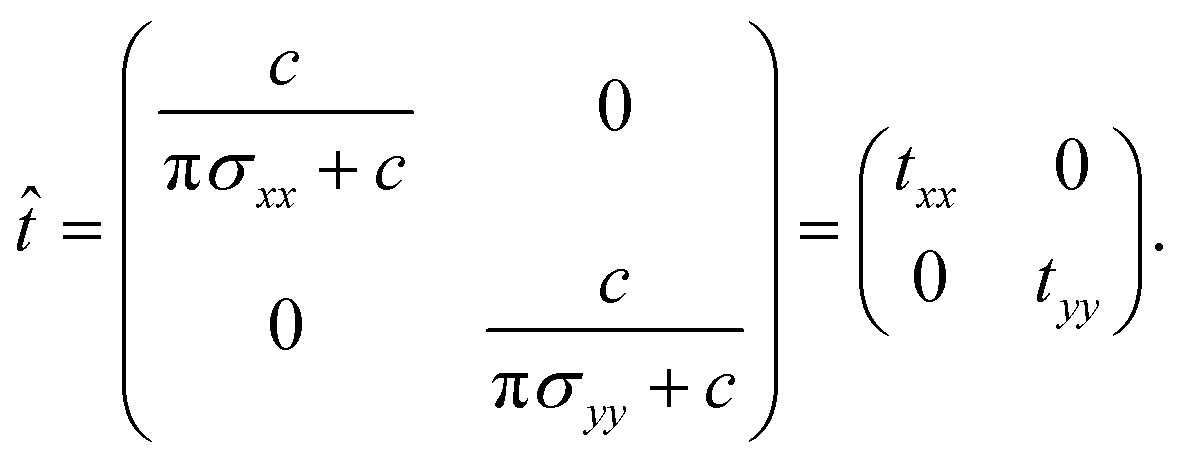 | (8b) |
For a right-circularly polarized electromagnetic wave, the incident elliptically polarized, the reflected and the transmitted electric fields are described by, respectively,
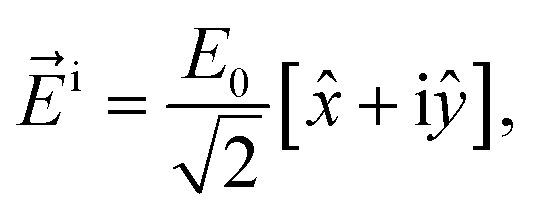 | (9a) |
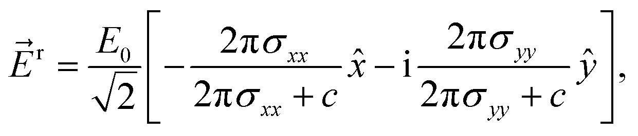 | (9b) |
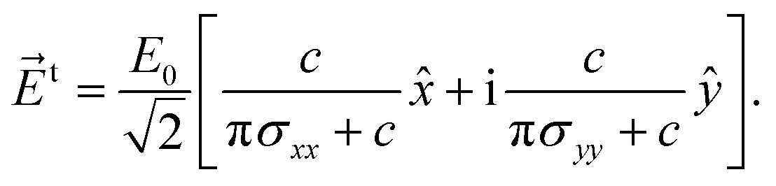 | (9c) |
According to the right-circularly (+) and left-circularly (−) handed polarizations coming from ![[p with combining circumflex]](https://www.rsc.org/images/entities/i_char_0070_0302.gif) = (
= (![[x with combining circumflex]](https://www.rsc.org/images/entities/i_char_0078_0302.gif) ± iŷ)/2,54 the general elliptically polarized wave can be written as = E++ + E−−. Under such conditions and data, the measure of ellipticity and the rotation angle of the polarization ellipse can be connected to the components E+ and E− with the help of relations
± iŷ)/2,54 the general elliptically polarized wave can be written as = E++ + E−−. Under such conditions and data, the measure of ellipticity and the rotation angle of the polarization ellipse can be connected to the components E+ and E− with the help of relations 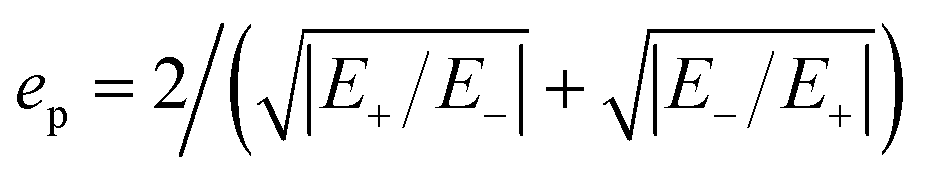 and αp = [arctan(ImE+/ReE+) − arctan(ImE−/ReE−)]/2, leading to the following relations in terms of reflection and transmission components:54
 | (10a) |
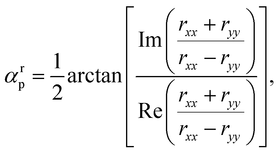 | (10b) |
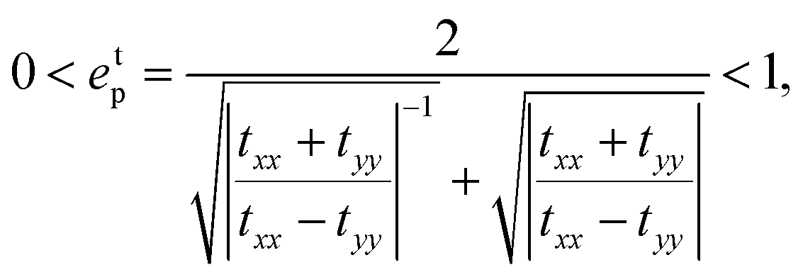 | (10c) |
 | (10d) |
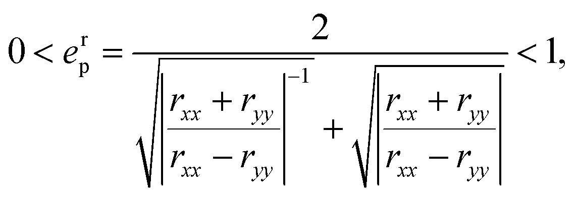
In eqn (10a) and (10c) two lower 0 and upper 1 limits correspond to the states of the circular and linear polarization of reflected and transmitted waves, respectively. On the other hand, eqn (10b) and (10d) refer to the amount of the ellipse axis rotation with respect to the x-direction, i.e. γ in Fig. 3. Another interesting quantity which the optical activity investigation completes is the positive absorbed wave intensity originating from the second law of thermodynamics, revealing the power dissipation defined by54
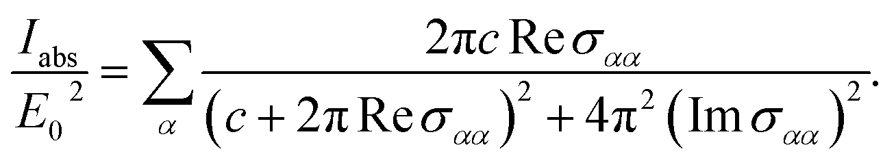 | (11) |
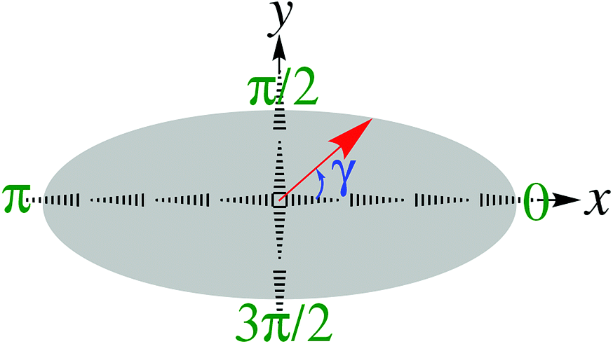 | ||
| Fig. 3 A schematic of the real-space distribution of reflected and transmitted elliptically polarized waves. The red arrow delimits the ellipse axis and its rotation angle with respect to the x-direction is denoted by the Greek symbol γ. | ||
Alternatively, we can pursue a route which allows us to calculate these parameters in the presence of uniaxial strain. These optical quantities are known in the literature under the keyword “optical activity”.
5 Discussion
In this section, we present our numerical results for monolayer black phosphorus based on tight-binding simulations within the linear response theory and Kubo formalism at finite temperature 10 K. The temperature effects are ignorable up to room temperature because the band gap of pristine phosphorene, 1.52 eV, is much larger than the room thermal energy kBT = 26 meV. The longitudinal optical conductivity components calculated in eqn (13) and (14) include only the interband transitions and the contribution of the intraband transitions are neglected because it is assumed that the incident optical field is strong enough and will be absorbed by carriers to satisfy energy and momentum conservation, leading to infinite momentum relaxation time. Thus, the Drude-like term is no longer relevant in the present paper.One could expect that the electron–hole coupling (exciton) effects are influential on the optical activity of phosphorene when an optical field is present. This is completely true but one needs to use many-body perturbation theory based on first-principles simulations, which is out of the scope of the current paper.
The main potential chemical insight of our results refers to the orbital and hybridization effects induced by applied strain on the interband optical conductivity of phosphorene. The sp3-hybridization of orbitals in phosphorene originating from three covalent σ-bonds and two out-of-plane (π-bond) orbitals leads to the unique puckered structure of phosphorene, which makes it very susceptible to deformations due to strain. The band gap of phosphorene largely originates from the out-of-plane pz-like orbitals. Therefore, when the height of the puckered structure slightly changes, the band gap of phosphorene alters. In fact, the change in the band gap implies that the electronic wave function spatial distribution and the overlap of orbitals in phosphorene have been changed depending on the modulus and direction of the strain. Thus, an increase or a decrease in the band gap of phosphorene under strain results from the strained overlap of orbitals.
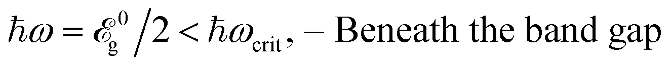
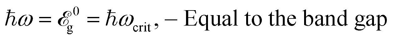
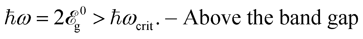
Generally, we divide the present section into three subsections in terms of the relation between the incident optical frequency and the band gap size of pristine phosphorene. In fact, here, we have introduced the criterion 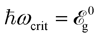 dependently from the band gap which leads to the definition of three regimes
 | (12a) |
 | (12b) |
 | (12c) |
In what follows, the physical constant ħ is set to unity for simplicity. Fig. 4–6 show the corresponding results, and a comparison between results for the frequency sets above-mentioned will be presented at the end. Before presenting the results we note some general descriptions to elucidate the physical meanings of parameters and expected treatments.
When a circularly polarized light hits the strained phosphorene’s plane in a normal direction, it may be of interest to see how the eccentricity ep and the phase shift αp of the reflected and transmitted electromagnetic waves behave with strain modulus and under which conditions the strain-induced modification of the optical activity of phosphorene is achieved. As is evident from eqn (13) and (14) the system consists of two different conductivities. Although the applied incident light is circularly polarized, however, these anisotropic conductivities, in turn, lead to elliptic reflected and transmitted waves, not circular. The stretching of the polarization ellipse is measured by the eccentricity ep with two lower and upper limit values corresponding to the linear and circular polarization, respectively. On the other hand, the phase shift αp is responsible for the amount of ellipse axis rotation with respect to the x direction. As pointed out in the introduction, the ultimate goal of this project is to find uniaxial strain effects on this stretching and ellipse axis rotation. However, these effects are not the same for the reflected and transmitted light and suggest that applied strain may be used to amplify the polarization.
We close these clarifications with some short remarks on the strain effects in view of microscopic physics. It is noteworthy to mention that the top of the valence band and the bottom of the conduction band in most 2D materials are dominated by the pz orbitals, i.e. out-of-plane spatial distribution. The real-space wave functions corresponding to these bands become compressed and tensioned for ε < 0 and ε > 0, respectively, leading to bonding and non-bonding states. These quantum effects manifest themselves in optical transitions and accordingly optical activities in general.
5.1 Beneath the band gap
To exploit the uniaxial strain effects on the ep and αp at frequencies smaller than the band gap, special frequency has been considered. With respect to the strain modulus, an illustration of the reflected, transmitted and absorbed quantities is shown in Fig. 4. As illustrated in Fig. 4, the eccentricity has always 0 and 1 as the lower and upper limit, respectively. To interpret the findings, we need some information from Fig. 2. In Fig. 2(b), below the band gap of 1.52 eV, both εx and εy behave similarly except at εy = −26%, while εz behaves differently with a dip at +12%. It is expected to have the same treatments once the optical frequency is located at this regime. While both εx and εy in Fig. 4 have almost the same trends, the εz one demonstrates another trend, as expected.
 | ||
Fig. 4 The reflected and transmitted eccentricity {(a) and (c)} and rotation angle {(b) and (d)} of the polarization ellipse, respectively, as a function of the strain modulus ε along different directions. These quantities are calculated at photon energy  . Panel (e) shows the intensity of the absorbed wave as a function of the strain modulus ε along different directions. The temperature is fixed at T = 10 K to generate these plots. . Panel (e) shows the intensity of the absorbed wave as a function of the strain modulus ε along different directions. The temperature is fixed at T = 10 K to generate these plots. | ||
In Fig. 4(a), we anticipate some results for the stretching of the reflected polarization ellipse when uniaxial strain is applied. At first glance, it is clear that the incident circularly polarized light is elliptically polarized when reflecting because 0 < erp < 1 and can be tuned with strain. With the compressive strain, the maximum stretching for erp is around 0.26 at εx(y) = −30(−22)%, whereas this occurs around 0.35 at εz = +10%. From compressive to tensile strain along all directions, the polarization of reflected light becomes almost circular except at the above-mentioned points. On the other hand, the ellipse axis of the reflected light, Fig. 4(b), changes with strains with γ < 90°. This implies that there is no sign change in αrp. For the strained ellipse axis, reflected light reports εx = −25%, εy = −18%, εz = +8%, and εz = +16% for which the reflected light confronts with big changes. Interestingly, the ellipse axis does not change when the compressive (tensile) strain is applied along the z (x/y) direction. In general, the dominant contribution of the compressive strain comes from the x and y directions, while the tensile strain along the z direction is responsible for ellipse axis alterations.
Concerning the implementation of these strains, since the monolayer phosphorene is a highly transparent 2D system,56,57 the stretching and rotating of transmitted light has to be slightly modified as well. Thus, it is expected that the system always keeps its initial polarization, i.e. circular, in the transmitted light, thereby etp has to be close to 1, as confirmed in Fig. 4(c). From the reflected light behavior, no changes have to be made to the etp for εx(y) < −18%(−14%) and +6% < εz < +18%. As a matter of fact, αtp must report the ellipse axis in another way. This implies that when αrp is negative, αtp must be positive, as illustrated in Fig. 4(d). Again, the compressive (tensile) strain along the z (x/y) direction prevents the ellipse axis rotation of transmitted light. However, this time, εx = −18%, εy = −14%, εz = +6%, and εz = +15% are responsible for the ellipse axis changes. Surprisingly, the transmitted light reaches an angle γ > 90° at εz > +20% because of the sign change of αtp. It should be pointed out that the results of small orders of magnitude in αtp do not allow us to estimate a significant change in ellipse axis rotation for the transmitted waves with strain as a direct consequence of the inherent transparency of phosphorene.
These plots are used for demonstrating the strained absorbed light evolution. It is seen from Fig. 4(e) that the intensity of the absorbed wave is so small and the maximum absorbed light is around (on average) 2% ∝ Iabs/E02 = 0.02, appearing at εx = −28%, εy = −22% and εz = +10%. The results almost coincide with the results of reflected and transmitted light, proving that the in-plane compressive strains mostly contribute to the absorption spectra as well, while the out-of-plane tensile strain dominates the absorbed light alterations with strain. These small intensities indicate the low tendency of phosphorene to absorb the incident electromagnetic wave with  .
.
Nevertheless, these competitions between strain modulus, eccentricity, and phase shift of incident circularly polarized light are not strongly unexpected because the optical excitations take the low-frequency limit into account in Fig. 4. Since only the interband transitions are included in eqn (13) and (14), the transitions refer to the inter-valence-band transitions only. If higher amounts of ħω are taken into account, one finds that the treatments become different. In the next subsection, we analyze the mid- and high-energy optical frequencies solely in terms of orientation-dependent strain modulus.
5.2 Equal to the band gap
We present the results obtained with the same manner for the optical energy . Similarly, the same evolutions are calculated targeting the direction-dependent strain effects on the optical activity of phosphorene when the optical field is strong enough to excite the electrons from the valence band to the conduction band. Fig. 5 shows that, on average, both compressive and tensile strains do not contribute significantly to the excitation and optical activity phenomena and again the in-plane compressive strains and out-of-plane tensile strains come in to play a role in controlling the stretching and rotating of the ellipse axis of both reflected and transmitted light. However, it is expected to have new insights into both strain effects for higher optical frequencies.
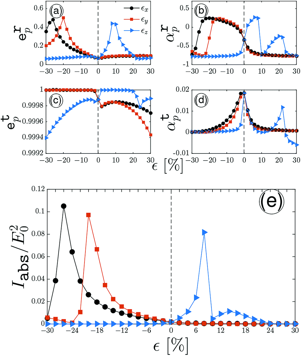 | ||
Fig. 5 The reflected and transmitted light stretching {(a) and (c)} and rotating {(b) and (d)} of the ellipse axis, respectively, as a function of the strain modulus ε along different directions at optical energy  and temperature T = 10 K. On the other hand, the strain-dependent intensity of absorbed light is plotted in panel (e). and temperature T = 10 K. On the other hand, the strain-dependent intensity of absorbed light is plotted in panel (e). | ||
The contribution of the strain along the armchair direction to the reflected erp in Fig. 5(a) indicates that the stretching of the ellipse axis has increased compared to the previous case. On average, while the minimum eccentricity of the reflected light takes place at 0.9 for all in-plane compressive and all out-of-plane tensile strains, the maximum eccentricity of the reflected light is 0.48 occurring at εx = −26%, εy = −20% and εz = +10%. One can see from Fig. 5(b) that this time, i.e. for  , while the ellipse axis changes can be seen clearly for in-plane compressive and out-of-plane tensile strains, an angle γ > 90° appears for −25% < εx < −2%, −19% < εx < −2% and +1% < εz < +9%. However, again, no ellipse axis change for all in-plane tensile and all out-of-plane compressive strains is reported.
In order to check the behavior of transmitted light for the optical frequency  , eqn (10c) and (10d) are plotted in Fig. 5(c) and (d) versus the strain modulus ε. Fig. 5(c) shows that the transmission is completely 100% for −25% < εx < −2%, −19% < εx < −2% and +1% < εz < +9%, as expected from the etp curves and there are little to no effects of in-plane tensile and out-of-plane compressive strains, which are negligible. This is due to the larger transmitted energy than the reflected one. In panel (d) of Fig. 5, αtp is plotted versus strain for various values of ε{x,y,z}. With the applied strain beginning at −30% independent of the direction, the phase shift increases with in-plane compressive strains up to zero percent strain and decreases forever. On the other hand, it does not change with the out-of-plane one up to εz = −6% and establishes an oscillation around a specific value εz = +10%, leading to an angle γ > 90° for εz > +25%.
The intensity of absorbed light at  is shown in Fig. 5(e). Similar behavior as in Fig. 4(e) appears, having gained zero intensity for both in-plane tensile and out-of-plane compressive strains. This means that the greatest contribution of absorption versus strain originates from the in-plane compressive and out-of-plane tensile strains. As there is enough excitation the absorption spectra should show a stronger response than before. Hence, Iabs/E02 should represent higher intensities than its initial values for all. Fig. 5(e) matches our expectation thus proving the accuracy of the formulation and numerical simulations. The maximum intensity of absorbed light is on average around 9 percent when the optical energy is equal to the band gap size.
5.3 Above the band gap
Now we extend the discussion from the low-optical energy to a higher regime. We expect effective behaviors to emerge for where very fast and robust transitions are found. For a more accurate statement, however, we need to reach an in-plane rotation and strong stretching so that the polarization can be fully circular even for the reflected light. This is predicted by Fig. 6 to take place at
  . Note that the low-energy two-band Hamiltonian model may fail to describe the system at frequencies larger than
  ; from this point, our model remains valid only for
  to be reliable. Our implementation of the large frequencies involves dynamic control of the number of transition states and a significant discrepancy between the results emerges.
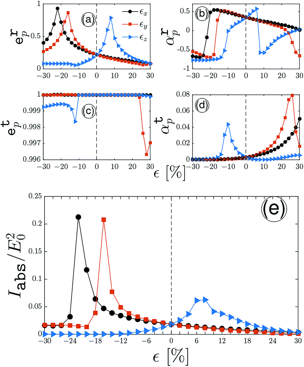 | ||
Fig. 6 Influence of the strain direction on the strain evolution of reflected {(a) and (b)}, transmitted {(c) and (d)} and absorbed (e) optical activity of single-layer black phosphorus at T = 10 K and  . . | ||
Starting from the reflected light, as usual, Fig. 6(a), the stretching of the ellipse axis is successively increased with strain and reaches an average of 0.85 at εx = −22%, εy = −16% and εx = +8%, very close to the circular polarization case. From a quick comparison between panels (a) of Fig. 4–6, it is evident that the eccentricity parameter increases with optical frequency. Most likely, the main advantage of the dynamic adjustment of this regime of optical frequency can be attributed to the contribution of both in-plane and out-of-plane compressive and tensile strains in the optical activity, in contrast to the two other regimes for which only the compressive or tensile strains mostly contributed. The curves presented in Fig. 6(b) clearly indicate the advantages of this optical frequency for the ellipse axis rotation of reflected light since a full rotation γ = 180° (sign change with almost the same values) appears at εx = −21%, εy = −17% and εx = +9%. On the other hand, the contribution of both strains is also supported by this figure.
With respect to the reflected eccentricity and phase shift parameters, the strain evolution of transmitted parameters performs best at  , too. Fig. 6(c) shows that the in-plane and out-of-plane strains do not change the incident circular polarization for −30% < εx = εy < +24% and −10% < εz < +30%, respectively. Even the order scales for the changes made are negligible. In contrast to the previous results, i.e. previous optical energy regimes, the out-of-plane compressive and in-plane tensile strains contribute mostly to the transmitted ellipse axis change, however, no full rotation is observed. Together with the advantages already addressed, the frequency
  appears to be very suitable for the study of the optical activity of strained phosphorene.
As for the improvement of absorption spectra, we quantitatively determined the strain-dependent intensity of absorbed light in Fig. 6(e). The discrepancy between the peaks for in-plane and out-of-plane strains prevents us to judge on average, however, 22% and 6% can be attributed at εx = −22%, εy = −16% and εz = +8%, respectively. Nevertheless, the dominant contributions of in-plane compressive and out-of-plane tensile strains remain unchanged even at high enough optical frequencies.
6 Summary
In the field of 2D optical materials, tuning of the reflected, transmitted and absorbed waves of incident electromagnetic waves is essential for some purposes. Only if a sufficiently suitable external factor can be applied, the optical activity, which exploits the special properties of a material, can be tuned. However, this involves some issues, making the tuning hard, in anisotropic materials like phosphorene.In this paper, we present a study of strain effects on the dynamics of charge carriers and eventually optical responses in phosphorene where the atomic orbitals’ spatial distribution when applying strain is responsible for these effects. During recent years, the two-band Hamiltonian model has proven to be a good description of the carrier dynamics in monolayer phosphorene. There, the strained two-band model is dominated by the Harrison relation between the hopping energies before and after strain. For studying the strain effects on the optical activity of phosphorene, we combine the two-band Hamiltonian model, the Harrison rule and the linear response theory. These methods capture the data for optical fields up to a certain degree and, for much higher optical fields, another model is necessary. Thus, this work is restricted to a certain optical field regime, namely beneath the band gap, equal to the band gap and above the band gap regimes. For this reason, the numerical simulations are separated to treat these three regimes.
Motivated by a simple analytic argument for the strain-induced band gap, the results for the optical activity of strained phosphorene are presented. The results first exhibit two phase transitions on increasing the strain modulus and on changing the strain orientation. The first transition occurs from semiconductor to metal, while the second one appears from semiconductor to semimetal for zigzag compressive strain and out-of-plane tensile strain, respectively. Using an analysis in the low-optical-field regime where only inter-valence-band transitions play a role, the intensity of reflected, transmitted and absorbed light is not significant, as expected.
Overall, from the low-optical-field limit to high-optical-field limit, the polarization of a reflected wave approaches the circular case and the reflected ellipse axis tends to a full rotation of γ = 180°. This behavior particularly depends on the strain modulus and direction. However, all curves of transmitted eccentricity reveal some small discrepancies with the optical field, but the relative deviation between the curves of the transmitted phase shift is significant. The value of strain also has an impact on these treatments as it controls the polarization and change/rotation of the ellipse axis. Next, the dependence of the intensity of absorbed light on the strain modulus and direction increases with optical energy and leads to larger absorption percentages. Quantitatively, these optical activity parameters are signaled by direction-dependent critical strains. This is interpreted as the effect of orbitals’ real-space distribution. But one has to keep in mind that for investigation of larger frequencies, another model is required to be simulated.
In a nutshell, we report rigorous and interesting results for the strain-induced optical activity of monolayer phosphorene and discuss the optical energy effects for which one is able to fully control strained phosphorene, offering an enormous amount of possibilities in finding new insights in phosphorene-based optoelectronic applications. Although a vast number of works are left to be considered by our group, a nice extension of the work in the future could focus on fine-tuning the band gap with atomic dopants on pristine and strained black phosphorous.
Appendix A: The diagonal terms of the interband optical conductivity tensor
In this appendix, we provide the diagonal terms of the interband optical conductivity tensor for the armchair direction
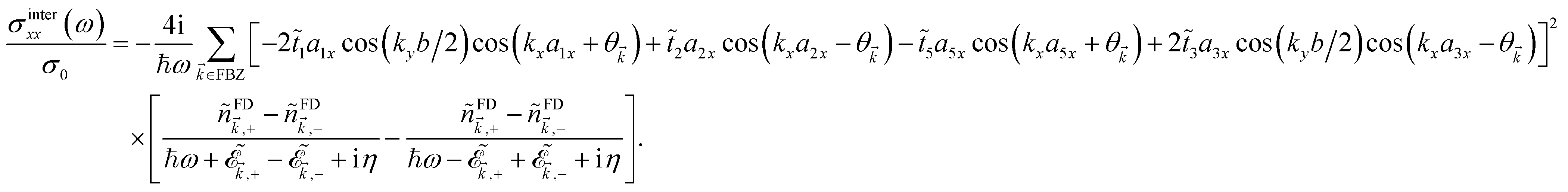 | (13) |
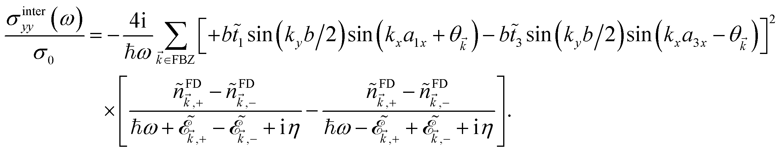 | (14) |
 stands for the strained Fermi–Dirac distribution function at the chemical potential μ and temperature T (kB being the Boltzmann constant). Also we used the definition eiθ =
 ![[g with combining tilde]](https://www.rsc.org/images/entities/i_char_0067_0303.gif) /|| for the phase θ in which is the strain-induced g.
/|| for the phase θ in which is the strain-induced g.
Conflicts of interest
There are no conflicts to declare.References
- K. S. Novoselov, A. K. Geim, S. V. Morozov, D. Jiang, Y. Zhang, S. V. Dubonos, I. V. Grigorieva and A. A. Firsov, Science, 2004, 306, 666 CrossRef CAS PubMed.
- K. S. Novoselov, A. K. Geim, S. V. Morozov, D. Jiang, M. I. Katsnelson, I. V. Grigorieva, S. V. Dubonos and A. A. Firsov, Nature, 2005, 438, 197 CrossRef CAS PubMed.
- K. S. Novoselov, Z. Jiang, Y. Zhang, S. V. Morozov, H. L. Stormer, U. Zeitler, J. C. Maan, G. S. Boebinger, P. Kim and A. K. Geim, Science, 2007, 315, 1379 CrossRef CAS PubMed.
- A. J. Mannix, X. F. Zhou, B. Kiraly, J. D. Wood, D. Alducin, B. D. Myers, X. Liu, B. L. Fisher, U. Santiago and J. R. Guest, Science, 2015, 350, 1513 CrossRef CAS PubMed.
- N. Takagi, C. L. Lin, K. Kawahara, E. Minamitani, N. Tsukahara, M. Kawai and R. Arafune, Prog. Surf. Sci., 2015, 90, 1 CrossRef CAS.
- F. F. Zhu, W. J. Chen, Y. Xu, C. L. Gao, D. D. Guan, C. H. Liu, D. Qian, S. C. Zhang and J. F. Jia, Nat. Mater., 2015, 14, 1020 CrossRef CAS PubMed.
- M. Derivaz, D. Dentel, R. Stephan, M. Hanf, A. Mehdaoui, P. Sonnet and C. Pirri, Nano Lett., 2015, 15, 2510 CrossRef CAS PubMed.
- A. Splendiani, L. Sun, Y. Zhang, T. Li, J. Kim, C. Y. Chim, G. Galli and F. Wang, Nano Lett., 2010, 10, 1271 CrossRef CAS PubMed.
- H. Liu, A. T. Neal, Z. Zhu, Z. Luo, X. Xu, D. Tomanek and P. D. Ye, ACS Nano, 2014, 8, 4033 CrossRef CAS PubMed.
- A. Castellanosgomez, L. Vicarelli, E. Prada, J. O. Island, K. L. Narasimhaacharya, S. I. Blanter, D. J. Groenendijk, M. Buscema, G. A. Steele and J. V. Alvarez, 2D Mater., 2014, 1, 025001 CrossRef.
- H. Liu, Y. Du, Y. Deng and P. D. Ye, Chem. Soc. Rev., 2015, 44, 2732 RSC.
- S. Das, M. Demarteau and A. Roelofs, ACS Nano, 2014, 8, 11730 CrossRef CAS PubMed.
- M. V. Kamalakar, B. N. Madhushankar, A. Dankert and S. P. Dash, Small, 2015, 11, 2209 CrossRef CAS PubMed.
- X. Wang, A. M. Jones, K. L. Seyler, V. Tran, Y. Jia, H. Zhao, H. Wang, L. Yang, X. Xu and F. Xia, Nat. Nanotechnol., 2015, 10, 517 CrossRef CAS PubMed.
- S. P. Koenig, R. A. Doganov, H. Schmidt, A. H. C. Neto and B. Ozyilmaz, Appl. Phys. Lett., 2014, 104, 103106 CrossRef.
- L. Li, Y. Yu, G. J. Ye, Q. Ge, X. Ou, H. Wu, D. Feng, X. H. Chen and Y. Zhang, Nat. Nanotechnol., 2014, 9, 372 CrossRef CAS PubMed.
- F. Xia, H. Wang and Y. Jia, Nat. Commun., 2014, 5, 4458 CrossRef CAS PubMed.
- T. Low, A. S. Rodin, A. Carvalho, Y. Jiang, H. Wang, F. Xia and A. H. Castro Neto, Phys. Rev. B: Condens. Matter Mater. Phys., 2014, 90, 075434 CrossRef.
- G. Zhang, S. Huang, A. Chaves, C. Song, V. O. Özçelik, T. Low and H. Yan, Nat. Commun., 2017, 8, 14071 CrossRef CAS PubMed.
- S. Yuan, A. N. Rudenko and M. I. Katsnelson, Phys. Rev. B: Condens. Matter Mater. Phys., 2015, 91, 115436 CrossRef.
- J. Chen, S. Chen and Y. Gao, J. Phys. Chem. Lett., 2016, 7, 2518 CrossRef CAS PubMed.
- A. Jain and A. J. H. McGaughey, Sci. Rep., 2015, 5, 8501 CrossRef CAS PubMed.
- Z.-Y. Ong, Y. Cai, G. Zhang and Y.-W. Zhang, J. Phys. Chem. C, 2014, 118, 25272 CrossRef CAS.
- D. Cakir, C. Sevik and F. M. Peeters, Phys. Rev. B: Condens. Matter Mater. Phys., 2015, 92, 165406 CrossRef.
- J. Kim, S. S. Baik, S. H. Ryu, Y. Sohn, S. Park, B.-G. Park, J. Denlinger, Y. Yi, H. J. Choi and K. S. Kim, Science, 2015, 349, 723 CrossRef CAS PubMed.
- R. Fei and L. Yang, Nano Lett., 2014, 14, 2884 CrossRef CAS PubMed.
- J.-W. Jiang and H. S. Park, Nat. Commun., 2014, 5, 4727 CrossRef CAS PubMed.
- Q. Liu, X. Zhang, L. Abdalla, A. Fazzio and A. Zunger, Nano Lett., 2015, 15, 1222 CrossRef CAS PubMed.
- T. Zhang, J.-H. Lin, Y.-M. Yu, X.-R. Chen and W.-M. Liu, Sci. Rep., 2015, 5, 13927 CrossRef CAS PubMed.
- Q. Wei and X. Peng, Appl. Phys. Lett., 2014, 104, 251915 CrossRef.
- X. Peng, Q. Wei and A. Copple, Phys. Rev. B: Condens. Matter Mater. Phys., 2014, 90, 085402 CrossRef.
- J.-W. Jiang and H. S. Park, Phys. Rev. B: Condens. Matter Mater. Phys., 2015, 91, 235118 CrossRef.
- B. Sa, Y.-L. Li, J. Qi, R. Ahuja and Z. Sun, J. Phys. Chem. C, 2014, 118, 26560 CrossRef CAS.
- N. D. Hien, M. Davoudiniya, K. Mirabbaszadeh, L. T. T. Phuong and M. Yarmohammadi, Chem. Phys., 2019, 522, 249 CrossRef CAS.
- A. N. Rudenko and M. I. Katsnelson, Phys. Rev. B: Condens. Matter Mater. Phys., 2014, 89, 201408(R) CrossRef.
- D. Cakir, H. Sahin and F. M. Peeters, Phys. Rev. B: Condens. Matter Mater. Phys., 2014, 90, 205421 CrossRef.
- B. Sa, Y.-L. Li, J. Qi, R. Ahuja and Z. Sun, J. Phys. Chem. C, 2014, 118(46), 26560 CrossRef CAS.
- C. H. Yang, J. Y. Zhang, G. X. Wang and C. Zhang, Phys. Rev. B, 2018, 97, 245408 CrossRef CAS.
- M. Ezawa, New J. Phys., 2014, 16, 115004 CrossRef.
- A. N. Rudenko, S. Yuan and M. I. Katsnelson, Phys. Rev. B: Condens. Matter Mater. Phys., 2015, 92, 085419 CrossRef.
- P. T. T. Le, K. Mirabbaszadeh, M. Davoudiniya and M. Yarmohammadi, Phys. Chem. Chem. Phys., 2018, 20, 25044 RSC.
- C. Wang, Q. Xia, Y. Nie and G. Guo, Appl. Phys. Lett., 2015, 117, 124302 Search PubMed.
- J. Zhao, R. Yu, H. Weng and Z. Fang, Phys. Rev. B, 2016, 94, 195104 CrossRef.
- W. A. Harrison, Elementary Electronic Structure, World Scientific, Singapore, 1999 Search PubMed.
- H. Tang, J. W. Jiang, B. S. Wang and Z. B. Su, Solid State Commun., 2009, 149, 82 CrossRef CAS.
- E. Taghizadeh Sisakht, F. Fazileh, M. H. Zare, M. Zarenia and F. M. Peeters, Phys. Rev. B, 2016, 94, 085417 CrossRef.
- K. Li and E. Cheng, Phys. E, 2018, 97, 335 CrossRef CAS.
- J. Quereda, et al., Nano Lett., 2016, 16, 2931 CrossRef CAS PubMed.
- L. Zhang and Y. Hao, Sci. Rep., 2018, 8, 6089 CrossRef PubMed.
- C. Li, Z. Xie, Z. Chen, N. Cheng, J. Wang and G. Zhu, Materials, 2018, 11, 304 CrossRef PubMed.
- L. Seixas, A. S. Rodin, A. Carvalho and A. H. Castro Neto, Phys. Rev. B: Condens. Matter Mater. Phys., 2015, 91, 115437 CrossRef.
- G. Mahan, Many Particle Physics, Plenum Press, New York, 1993 Search PubMed.
- G. Grosso and G. P. Parravicini, Solid State Physics, Academic Press, New York, 2nd edn, 2014 Search PubMed.
- J. D. Jackson, Classical Electrodynamics, Wiley, New York, 1999 Search PubMed.
- R. Kubo, J. Phys. Soc. Jpn., 1957, 12, 570 CrossRef.
- G. T. Adamashvili, Tech. Phys. Lett., 2018, 44(4), 351 CrossRef CAS.
- C. K. Borah, P. K. Tyag, S. Kumar and K. Patel, Comput. Mater. Sci., 2018, 151, 65 CrossRef CAS.
| This journal is © The Royal Society of Chemistry 2019 |