DOI:
10.1039/C9RA01738K
(Paper)
RSC Adv., 2019,
9, 14422-14431
Bi2Te3 single crystals with high room-temperature thermoelectric performance enhanced by manipulating point defects based on first-principles calculation†
Received
7th March 2019
, Accepted 22nd April 2019
First published on 8th May 2019
Abstract
Intrinsic Bi2Te3 is a representative thermoelectric (TE) material with high performance at low temperature, which enables applications for electronic cooling. However, antisite defects easily form in p-type Bi2Te3, resulting in the difficulty of further property enhancement. In this work, the formation energy of native point defects in Bi2Te3 supercells and the electronic structure of Bi2Te3 primitive unit cell were calculated using first-principles. The antisite defect Bi_Te1 has a lower formation energy (0.68 eV) under the Te-lack condition for p-type Bi2Te3. The effects of point defects on TE properties were investigated via a series of p-type Bi2Te3−x (x = 0, 0.02, 0.04, 0.06, 0.08) single crystals prepared by the temperature gradient growth method (TGGM). Apart from the increased power factor (PF∥) which originates from the increased carrier concentration (n∥) and m*, the thermal conductivity (κ∥) was also cut down by the increased point defects. Benefitting from the high PF∥ of 4.09 mW m−1 K−2 and the low κ∥ of 1.77 W m−1 K−1, the highest ZT∥ of 0.70 was obtained for x = 0.06 composition at 300 K, which is 30% higher than that (0.54) of the intrinsic Bi2Te3.
1. Introduction
Thermoelectric (TE) materials have been investigated for use in power generation and semiconductor refrigeration based on the Seebeck and Peltier effects for decades, and are considered as a promising candidate to remit the energy shortages and environmental issues.1–3 However, the poor properties and conversion efficiencies of TE materials limit their applications on a world-wide scale. The conversion efficiencies of TE materials are determined by the dimensionless figure of merit, ZT = α2σT/κ, where α, σ, T and κ are the Seebeck coefficient, the electrical conductivity, the absolute temperature and the thermal conductivity, respectively.4,5 A high ZT value requires a high power factor (PF = α2σ) and a low κ. Research aimed at increasing PF values in recent decades is focused on optimizing and stabilizing the carrier concentration (n),6,7 engineering distortions of the electronic density of states near the Fermi energy (resonant levels)8,9 and achieving band convergence.10–12 The κ value can be significantly reduced by introducing point defects, dislocations and nanostructures.13–15
Intrinsic Bi2Te3 is a representative TE material with high performance at low temperature, which enables applications for electronic cooling.16,17 Bi2Te3 with a space group of R![[3 with combining macron]](https://www.rsc.org/images/entities/char_0033_0304.gif) m shows a lamella structure which consists of a five atomic layer in the order of Te1–Bi–Te2–Bi–Te1 along the c axis as shown in Fig. S1a.† The Bi2Te3 unit cell contains one type of Bi site (0.0000, 0.0000, 0.4000) and two types of Te sites (Te1 (0.0000, 0.0000, 0.2095) and Te2 (0.0000, 0.0000, 0.0000)).18,19 The intralayer bonds of Bi2Te3 are covalent while the interlayer bonds are the van der Waals interaction force and hybrids of the electrostatic interaction.20 The first work of Bi2Te3 as a TE material for refrigeration was reported in 1954 by Goldsmid.21 In the last decades, the TE properties of Bi2Te3 polycrystals were enhanced by point defects,22–24 textures25–27 and dislocation arrays28 and further optimized by alloying with isostructural Sb2Te3 (ref. 9–31) or Bi2Se3.22,32 The ZT of Bi0.5Sb1.5Te3 was dramatically increased to 1.86 at 320 K via full-spectrum phonon scattering which has a minimal charge-carrier scattering.28 In fact, producing point defects is convenient and effective to develop high-performance TE materials, which can simultaneously optimize the electrical transport properties and lattice thermal conductivity. However, the enhancement of TE performance via manipulating point defects in polycrystals is hard to understand rather than in single crystals. Preparations of Bi2Te3-based single crystals are usually achieved by the Bridgman33–35 and Zone Melting (ZM)36–38 methods, which need to move or rotate the crystal growth device and supply an inert atmosphere. A simple and convenient temperature gradient growth method (TGGM) only needs a vertical furnace compared with Bridgman and ZM, which has been provided to prepare high-performance SnSe single crystal as described by Duong et al.39 And the preparation of Bi2Te3 single crystal by TGGM was only reported in Mn-doped40 and Cu-doped41 Bi2Te3, but didn't detailedly investigate the TE properties of Bi2Te3. This motivates us to prepare Bi2Te3-based single crystals by TGGM method and investigate the effects of native point defects on TE properties.
m shows a lamella structure which consists of a five atomic layer in the order of Te1–Bi–Te2–Bi–Te1 along the c axis as shown in Fig. S1a.† The Bi2Te3 unit cell contains one type of Bi site (0.0000, 0.0000, 0.4000) and two types of Te sites (Te1 (0.0000, 0.0000, 0.2095) and Te2 (0.0000, 0.0000, 0.0000)).18,19 The intralayer bonds of Bi2Te3 are covalent while the interlayer bonds are the van der Waals interaction force and hybrids of the electrostatic interaction.20 The first work of Bi2Te3 as a TE material for refrigeration was reported in 1954 by Goldsmid.21 In the last decades, the TE properties of Bi2Te3 polycrystals were enhanced by point defects,22–24 textures25–27 and dislocation arrays28 and further optimized by alloying with isostructural Sb2Te3 (ref. 9–31) or Bi2Se3.22,32 The ZT of Bi0.5Sb1.5Te3 was dramatically increased to 1.86 at 320 K via full-spectrum phonon scattering which has a minimal charge-carrier scattering.28 In fact, producing point defects is convenient and effective to develop high-performance TE materials, which can simultaneously optimize the electrical transport properties and lattice thermal conductivity. However, the enhancement of TE performance via manipulating point defects in polycrystals is hard to understand rather than in single crystals. Preparations of Bi2Te3-based single crystals are usually achieved by the Bridgman33–35 and Zone Melting (ZM)36–38 methods, which need to move or rotate the crystal growth device and supply an inert atmosphere. A simple and convenient temperature gradient growth method (TGGM) only needs a vertical furnace compared with Bridgman and ZM, which has been provided to prepare high-performance SnSe single crystal as described by Duong et al.39 And the preparation of Bi2Te3 single crystal by TGGM was only reported in Mn-doped40 and Cu-doped41 Bi2Te3, but didn't detailedly investigate the TE properties of Bi2Te3. This motivates us to prepare Bi2Te3-based single crystals by TGGM method and investigate the effects of native point defects on TE properties.
In this work, we expect to prepare Bi2Te3 single crystals by TGGM method and enhance the TE properties of Bi2Te3 via combining an optimized carrier concentration with a reduced thermal conductivity. A series of p-type Bi2Te3−x (x = 0, 0.02, 0.04, 0.06, 0.08) single crystals were successfully prepared by applying TGGM. The phase structure, microstructures, and TE transport properties of Bi2Te3−x (x = 0, 0.02, 0.04, 0.06, 0.08) single crystals were investigated carefully. The electrical transport properties calculated by BoltzTraP2,42 and the electronic structure and the formation energy were associated to well understand the variation of TE properties for Bi2Te3 single crystals. The carrier concentration of in-plane (n∥) was significantly improved by adjusting the amount of Te. Owing to the increase of PF∥ (power factor of in-plane) and the reduction of κ∥ (thermal conductivity of in-plane), a significantly enhanced ZT∥ (ZT of in-plane) was achieved.
2. Method
2.1 Computational details
A plane-wave pseudopotential method in the Vienna ab initio Simulation Package (VASP) was used to achieve the density functional theory (DFT) calculations.43,44 The exchange and correlation function was described via Perdew–Burke–Ernzerhof generalized gradient approximation (GGA-PBE).45 The projector augmented wave (PAW) potentials were applied to describe the interaction between electrons and ions.46 The DFT-D3 method with Becke–Jonson damping implemented in the VASP code was used to describe the van der Waals interaction within the PBE function.47,48 By considering van der Waals forces and spin–orbit coupling (SOC), the electronic structure of Bi2Te3 primitive unit cell (Fig. S1c†) was calculated along the special lines connecting the high-symmetry points P (0.822852, 0.338574, 0.338574), a (0.661426, 0.419287, 0.419287), Γ (0, 0, 0), Z (0.5, 0.5, 0.5), Γ (0, 0, 0), L (0.5, 0.5, 0) according to the report of Brillouin zone by Setyawan et al.49 as shown in Fig. S1b.† The inertial effective masses  ,
,  and
and  of holes along different principal axes were calculated as defined in eqn (1):50,51
| |
 | (1) |
here, ℏ is the reduced Planck constant, x, y, z represent the directions in the reciprocal Cartesian space, En(k) is the dispersion relation for the n-th electronic band.
The calculation of formation energy was performed with a plane-wave cutoff of 500 eV and a 5 × 5 × 5 Monkhorst–Pack k-mesh basing on the 2 × 2 × 2 perfect and defective Bi2Te3 supercells. The defective supercells contain vacancies on the Bi (V_Bi), Te1 (V_Te1) and Te2 (V_Te2) sublattices and antisite defects on Te1 (Bi_Te1), Te2 (Bi_Te2) and Bi (Te_Bi) sublattices. The total energy converged to 1.0 × 10⁻⁴ eV and the Hellman–Feynman force was smaller than −1.0 × 10⁻² eV Å−1 in the optimized structures. The crystal of Bi2Te3 obtained from the Inorganic Crystal Structure Database (ICSD) (RmH, a = b = 4.39 Å and c = 30.50 Å) was taken as initial geometry. The formation energy (ΔEF) of Bi2Te3 with a native point defect (D) can be calculated as defined in eqn (2):52–55
| |
 | (2) |
where
ED and
Ebulk are the total energy of the defective supercell containing the defect
D and the perfect supercell, respectively;
ni is the number of change for i type atom such as Bi or Te and
ni should be >0 or <0 when i type atom is added or removed from the supercell;
μi represents the corresponding chemical potential of the i type atom;
q is the charge of the defect and
Ef is the Fermi level. In this work, the variation of
qEf is ignored. The rhombohedral phase of Bi and the trigonal phase of Te were used as the reference elemental bulk phases for the chemical potentials.
2.2 Sample preparation
Commercial powders of Bi (99.99%) and Te (99.999%) were weighed according to the chemical formula of Bi2Te3−x (x = 0, 0.02, 0.04, 0.06, 0.08). The powders were mixed manually for 30 minutes under an agate mortar using pestle and pressed into disks. The disks were loaded into quartz ampoules and flame-sealed at a pressure of 2–3 × 10⁻³ Pa. Another bigger quartz ampoule was sealed to prevent the inner ampoule from breaking during sintering. The quartz ampoules were slowly heated (10 K h−1) up to 913 K and soaked for 30 h at 913 K. Finally, the quartz ampoules were slowly cooled (1 K h−1) to 733 K and then to room temperature by furnace cooling. The schematic diagram of the preparation process for Bi2Te3−x single crystals by the TGGM is shown in Fig. S2.†
2.3 Characterization
The X-ray diffraction (XRD, SmartLab, Japan) with Cu Kα radiation was used to identify the phase structure. The observation of morphology for the single crystals was achieved via a field emission scanning electron microscope (FESEM, SUPRA™ 55, Germany). The transmission electron microscopy (TEM), high-resolution (HRTEM) images and the selected area electron diffraction (SAED) pattern were obtained by a transmission electron microscope (JEOL 2100F, Japan). The obtained single crystal was cut into bar-shaped samples with dimensions ca. 7.00 mm × 2.20 mm × 2.20 mm for electronic property measurements and square planar samples ca. 6.00 mm × 6.00 mm × 1.10 mm for the measurements of thermal diffusivity along different directions (out-plane, in-plane). The electrical conductivity (σ) and Seebeck coefficient (α) were measured in a helium atmosphere as increasing temperature from 300 K to 573 K via a Seebeck coefficient/electric resistance measuring system (Cryoall CTA-3, China). A Hall measurement system (ResiTest 8340DC, Tokyo, Japan) was applied to measure the Hall coefficient (RH). According to n = 1/(eRH) and μ = RH/ρ, the carrier concentration (n) and mobility (μ) were computed. The laser flash method (Netzsch LFA457, Germany) was applied to measure the thermal diffusivity (D). The specific heat Cp was estimated according to the Dulong–Petit limit. The Archimedes method was used to estimate the mass density (d). The total thermal conductivity (κ) was computed using κ = DCpd. All physical quantities of in-plane and out-plane were indicated by subscripts of ∥ and ⊥ to represent parallel and perpendicular to cleavage plane, respectively.
3. Results and discussion
3.1 Electronic structure calculation
Fig. 1 shows the band structure, total density of state (TDOS) and projected density of state (PDOS) for the intrinsic Bi2Te3. The valence band maxima (VBM) for Bi2Te3 is located at (0.51, 0.32, 0.32) along the a → Γ direction, while the conduction band minima (CBM) is located at (0.50, 0.50, 0.38) along the Z → F direction as shown in Fig. 1a. Bi2Te3 has a strong spin–orbit coupling (SOC) near the Fermi level due to the presence of the Bi 6p states, which can produce a low band gap (Eg).56,57 Herein, the calculated Eg 0.08 eV of Bi2Te3 is lower than the band gap obtained from experiments (0.13–0.16 eV),58,59 but it is well consistent with the literature calculated data (0.05–0.09 eV).57,60,61 The band structure is very similar to the early reports.62–64 The inertial effective masses  ,
,  and
and  of holes along the different principal axes were calculated to be 0.31 m0, 0.04 m0 and 0.04 m0, respectively, indicating that the TE properties of p-Bi2Te3 may be anisotropic.
 |
| | Fig. 1 (a) The band structure along the high-symmetry points P–a–Γ–Z–F–Γ–L, (b) the total density of state (TDOS), and (c–f) projected density of state (PDOS) for the intrinsic Bi2Te3. | |
The valence electrons of Bi and Te are treated explicitly as 15 (5d106s26p3) and 6 (5s25p4), respectively. As shown in Fig. 1c, Bi atoms play a dominant role to the PDOS near the CBM, indicating that Bi atoms will lose electrons and compose the conduction bands. On the other hand, Te1 and Te2 atoms contribute most to the PDOS near the VBM, which indicates that Te atoms will receive electrons and compose the valence bands.65 Fig. 1d shows that only the 6p orbitals of Bi atoms predominate near the CBM, while the Bi-6s and Bi-6p orbitals have a strong combined contribution near the VBM. Te1-5p and Te2-5p orbitals predominate both in the CMB and VBM as shown in Fig. 1e and f.
Fig. 2 shows the chemical potential dependence of electrical transport properties for Bi2Te3 along the in-plane and out-plane, which is simply evaluated by the BoltzTraP2. The chemical potential (μ–μ0) represents the doping level near the Fermi energy and τ is the relax time. (σ/τ)∥ of both p-type and n-type Bi2Te3 at 300 K is higher than that of (σ/τ)⊥ when the doping level is low as shown in the inset of Fig. 2a, which means the σ is anisotropic.66 However, the curves of α∥ and α⊥ are similar in Fig. 2b, indicating the isotropy of α. Due to the higher (σ/τ)∥, the power factor (α2σ/τ)∥ in Fig. 2c is higher than (α2σ/τ)⊥ when the doping level is low, which is coincided with the experiment data in Fig. 5 and S4.† What's more, the electrical transport properties of p-type Bi2Te3 are superior to that of n-type Bi2Te3 according to Fig. 2c.62
 |
| | Fig. 2 Chemical potential dependence of (a) electrical conductivity/relax time (σ/τ) calculated by BoltzTraP2, (b) Seebeck coefficient (α), and (c) power factor/relax time (α2σ/τ) for the intrinsic Bi2Te3 along the in-plane (∥) and out-plane (⊥) at 300 K. | |
3.2 Formation energy calculation
Formation energy (ΔEF) of native point defects V_Bi, V_Te1, V_Te2, Bi_Te1, Bi_Te2 and Te_Bi in Bi2Te3 for Te-lack condition is listed in Table 1, which is 2.48, 1.20, 1.51, 0.68, 1.14 and 1.54 eV, respectively. The calculated ΔEF indicates that the antisite defect Bi_Te1 is the easiest to form and will play a dominant role in Bi2Te3 under the Te-lack condition. However, for the Bi-lack condition, ΔEF of native point defects V_Bi, V_Te1, V_Te2, Bi_Te1, Bi_Te2 and Te_Bi in Bi2Te3 is 2.00, 1.52, 1.83, 1.48, 1.94 and 0.75 eV, respectively, implying that Te_Bi will predominate in Bi2Te3 under the Bi-lack condition.67
Table 1 Formation energy of native point defects in Bi2Te3 under Te-lack and Bi-lack conditions calculated using DFT
| Native point defects in Bi2Te3 |
Total energy of Bi2Te3 (Ebulk), eV |
Chemical potential of Bi (μBi), eV |
Chemical potential of Te (μTe), eV |
Native point defects in Bi2Te3 |
| V_Bi |
V_Te1 |
V_Te2 |
Bi_Te1 |
Bi_Te2 |
Te_Bi |
| Total energy, (ED), eV |
−149.07 |
−4.05 |
−3.14 |
−142.46 |
−144.41 |
−144.10 |
−149.05 |
−148.59 |
−146.86 |
| Formation energy (ΔEF), (eV) |
Te-lack |
— |
−4.13 |
−3.46 |
2.48 |
1.20 |
1.51 |
0.68 |
1.14 |
1.54 |
| Bi-lack |
— |
−4.60 |
−3.14 |
2.00 |
1.52 |
1.83 |
1.48 |
1.94 |
0.75 |
The lattice constants and unit cell volumes obtained from the optimized structures are listed in Table 2. The lattice constants (a = b, c) and unit cell volume (a × b × sin![[thin space (1/6-em)]](https://www.rsc.org/images/entities/char_2009.gif) γ × c) of the Bi2Te3 are 4.39 Å, 30.34 Å and 505.30 Å3, respectively. The reduction of a and c results in smaller unit cell volumes of defective Bi2Te3 with V_Bi, V_Te1, V_Te2, Bi_Te1 and Bi_Te2, which are 490.22, 497.66, 497.17, 503.35 and 502.89 Å3 respectively. It is worth to note that the lack of Bi can generate a significant variation in unit cell volume, while the changes of volumes from the antisite defects are relatively small. However, the a of Bi2Te3 with the defect Te_Bi is increased along with a decreased c, which has a unit cell volume of 501.80 Å3. The Fermi level relative to the reference level defined in the pseudopotentials is 6.39 eV for Bi2Te3 and decreases to 6.02, 6.15 and 6.18 eV for Bi2Te3 containing the defects of V_Bi, Bi_Te1 and Bi_Te2, respectively, implying that V_Bi, Bi_Te1 and Bi_Te2 would act as p-type dopants. On the contrary, the Fermi level of Bi2Te3 with the defects of V_Te2 and Te_Bi turns into 6.46 and 6.81 eV, respectively, which indicates V_Te2 and Te_Bi would act as n-type dopants. Although the Fermi level 6.31 eV of V_Te1 is slightly lower than that (6.39 eV) of Bi2Te3, V_Te1 should also be a n-type dopant. The reason for this result may be that the band structures of defective and perfect supercells were not lined up.
γ × c) of the Bi2Te3 are 4.39 Å, 30.34 Å and 505.30 Å3, respectively. The reduction of a and c results in smaller unit cell volumes of defective Bi2Te3 with V_Bi, V_Te1, V_Te2, Bi_Te1 and Bi_Te2, which are 490.22, 497.66, 497.17, 503.35 and 502.89 Å3 respectively. It is worth to note that the lack of Bi can generate a significant variation in unit cell volume, while the changes of volumes from the antisite defects are relatively small. However, the a of Bi2Te3 with the defect Te_Bi is increased along with a decreased c, which has a unit cell volume of 501.80 Å3. The Fermi level relative to the reference level defined in the pseudopotentials is 6.39 eV for Bi2Te3 and decreases to 6.02, 6.15 and 6.18 eV for Bi2Te3 containing the defects of V_Bi, Bi_Te1 and Bi_Te2, respectively, implying that V_Bi, Bi_Te1 and Bi_Te2 would act as p-type dopants. On the contrary, the Fermi level of Bi2Te3 with the defects of V_Te2 and Te_Bi turns into 6.46 and 6.81 eV, respectively, which indicates V_Te2 and Te_Bi would act as n-type dopants. Although the Fermi level 6.31 eV of V_Te1 is slightly lower than that (6.39 eV) of Bi2Te3, V_Te1 should also be a n-type dopant. The reason for this result may be that the band structures of defective and perfect supercells were not lined up.
Table 2 Lattice constants and the Fermi level of defective Bi2Te3 calculated using DFT
| Point defect |
a = b (Å) |
c (Å) |
α = β (°) |
γ (°) |
Unit cell volume (Å3) |
Fermi level (eV) |
| Bi2Te3 |
4.39 |
30.34 |
90 |
120 |
505.30 |
6.39 |
| V_Bi |
4.34 |
30.00 |
490.22 |
6.02 |
| V_Te1 |
4.36 |
30.22 |
497.66 |
6.31 |
| V_Te2 |
4.37 |
30.03 |
497.17 |
6.46 |
| Bi_Te1 |
4.38 |
30.32 |
503.35 |
6.15 |
| Bi_Te2 |
4.38 |
30.27 |
502.89 |
6.18 |
| Te_Bi |
4.40 |
29.89 |
501.80 |
6.81 |
3.3 Microstructure and phase characterizations
Fig. 3 shows the typical TEM and high-resolution TEM (HRTEM) images of x = 0 bulk. The TEM image without obvious grain boundary in a large scale is shown in Fig. 3a. The selected area electron diffraction (SAED) pattern of x = 0 bulk in the inset of Fig. 3a shows a clear lattice structure, which indicates the good crystallization of the bulk. The lattice spacings of 0.2228 and 0.2167 nm in the HRTEM image as shown in Fig. 3b correspond to (01![[1 with combining macron]](https://www.rsc.org/images/entities/char_0031_0304.gif) 11) and (11
11) and (11![[2 with combining macron]](https://www.rsc.org/images/entities/char_0032_0304.gif) 0) planes of Bi2Te3, respectively.
0) planes of Bi2Te3, respectively.
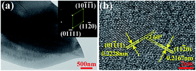 |
| | Fig. 3 (a) TEM image and the SAED pattern and (b) HRTEM image for the x = 0 bulk. | |
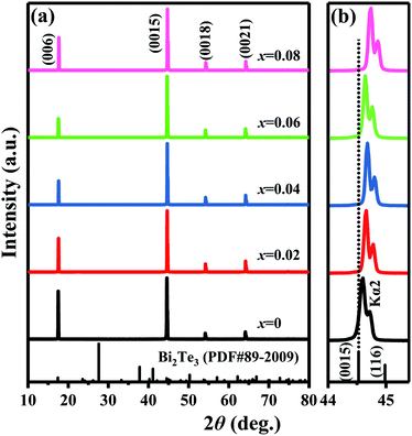
Fig. 4 shows the XRD patterns of cleavage planes for Bi2Te3−x (x = 0, 0.02, 0.04, 0.06, 0.08) single crystals. Only (00l) diffraction peaks can be observed in all the XRD patterns, indicating that the Bi2Te3−x single crystal whose crystallographic c axis is perpendicular to the cleavage plane were synthesized. The field emission scanning electron microscope (FESEM) images in Fig. S3† exhibit a layered micro-structure with an average thickness about 1 μm, and the energy dispersive spectrometer (EDS) mapping indicates that compositional distribution of Bi and Te is very uniform for x = 0 single crystal with an atomic ratio of Bi:Te = 59.69:40.31. In order to analyse the variation of lattice constants and point defects, the rhombohedral Bi2Te3 (Rm, PDF#89–2009) was chosen as a reference. To analyse the influences of insufficient Te on the lattice variation of the host Bi2Te3 phase, the 2θ angle of the strongest diffraction peak (0015) (abbreviated as 2θ(0015)) is highlighted in Fig. 4b. The shoulder peak next to (0015) diffraction peak comes from the diffraction of Cu Kα2 line.68 The 2θ(0015), interplanar spacing of the strongest diffraction peak (0015) (abbreviated as d(0015)) and lattice constant of c axis are shown in Table 3. The 2θ(0015) shifts from 44.60° to 44.68° when x increases from 0 to 0.04 and is higher than that (44.53°) of the standard card (Bi2Te3, PDF#89–2009), which corresponds to the decrease of lattice constant c from 30.45 Å to 30.40 Å. The 2θ(0015) decreases to 44.64° at x = 0.06, which has a trend of returning to 44.53° of the standard card, but turns to higher angle (44.74°) by further increasing x to 0.08. At the same time, the lattice constant c increases to 30.42 Å at x = 0.06, then reduces to 30.36 Å at x = 0.08.
 |
| | Fig. 4 XRD patterns of cleavage planes for Bi2Te3−x (x = 0, 0.02, 0.04, 0.06, 0.08) single crystal at (a) 10–80° and (b) 44–45.4°. | |
Table 3 The 2θ angle (2θ(0015)), the interplanar spacing (d(0015)) of the strongest diffraction peak (0015) and lattice constant c for Bi2Te3−x (x = 0, 0.02, 0.04, 0.06, 0.08) samples
| Sample |
PDF#89-2009 |
x = 0 |
x = 0.02 |
x = 0.04 |
x = 0.06 |
x = 0.08 |
| 2θ(0015) (°) |
44.53 |
44.60 |
44.66 |
44.68 |
44.64 |
44.74 |
| d(0015) (Å) |
2.0331 |
2.0300 |
2.0275 |
2.0265 |
2.0281 |
2.0240 |
| c (Å) |
30.50 |
30.45 |
30.41 |
30.40 |
30.42 |
30.36 |
The native point defects in the intrinsic p-type Bi2Te3 include V_Bi, V_Te and Bi_Te,23,24 which can be described as eqn (3)–(5), where y and z are the content of volatilization for Bi and Te during the sintering process. According to Table 2 and eqn (3), the volatilization of Bi can produce negatively charged vacancy  and extra holes (h˙), causing a large decrement of lattice constants for Bi2Te3. The volatilization of Te can generate positively charged vacancy
  and extra electrons (e′) as described in eqn (4). The formation of
  is easier than
  during the sintering process because of the lower energy of evaporation for Te (52.55 kJ mol−1) compared with Bi (104.80 kJ mol−1). So, eqn (4) plays a dominant role, which is coincided quite well with the calculation of formation energy in Table 1. However, the close electronegativity between Bi (2.02) and Te (2.01) makes it easy for Bi to jump to the Te-sites, forming antisite defects along with h˙ generated as shown in eqn (5). What's more,
  and
and  can cancel each other out with a ratio of 2:3, as described in eqn (5).
Hence, the increased 2θ(0015) at 0 ≤ x ≤ 0.04 is attributed to the substitution of Te2− (r = 2.21 Å) by Bi3+ (r = 0.96 Å) which can shrink the lattice of Bi2Te3 as shown in Tables 2 and 3 and increase the h˙ concentration as shown in Fig. 6a. When x = 0.06, eqn (5) still plays a dominant role in Bi2Te3 and increases n∥. However, a small amount of Bi may fill into  and fix h˙ as described in eqn (6) and enlarge the lattice of Bi2Te3 as shown in Fig. 4b. With the further lack of Te, the effect of eqn (5) is enhanced while the function of eqn (6) is limited, resulting in the shrinkage of Bi2Te3 lattice in Fig. 4b and the enhancement of n∥ in Fig. 6a. According to the above analysis, the point defect Bi_Te plays a dominant role in all Bi2Te3 bulks and leads to the decrease of lattice constant c as shown in Table 3, which is corresponding to the reduction of lattice constant c from DFT calculation as shown in Table 2.
| |
 | (3) |
| |
 | (4) |
| |
 | (5) |
| |
 | (6) |
3.4 TE transport properties
Fig. 5 shows the TE transport properties of x = 0 bulk along the in-plane and out-plane. σ∥ of x = 0 in Fig. 5a decreases from 3.87 × 10⁴ S m−1 (300 K) to 3.38 × 10⁴ S m−1 (342 K), and then increases to 7.02 × 10⁴ S m−1 (573 K) in the whole measured temperature ranging from 300 K to 573 K. σ⊥ has the same variation with σ∥. The lower σ⊥ compared to σ∥ is attributed to a lower carrier mobility (μ⊥) for the interlayer direction. α∥ and α⊥ in Fig. 5b decrease with an increase of temperature. α∥ changes from positive to negative between 400 K and 500 K, meaning the transformation of p-type to n-type semiconductor, while α⊥ is positive in the whole measured temperature. The anisotropy of α may be attributed to the ratio of the mobility of holes to the mobility of electrons is different along the in-plane and out-plane, which is also reported by Situmorang69 and Dennis.70 A highest PF∥ 3.37 mW m−1 K−2 is obtained at 300 K as shown in Fig. S4a.† The anisotropy of TE properties for Bi2Te3 corresponds well with the calculation results in Fig. 2.
 |
| | Fig. 5 Temperature dependence of TE properties along the in-plane (∥) and out-plane (⊥) for x = 0 bulk. (a) Electrical conductivity (σ), (b) Seebeck coefficient (α), (c) total thermal conductivity (κ) and the sum of lattice thermal conductivity and bipolar thermal conductivity (κlat + κbip), and (d) figure of merit (ZT). | |
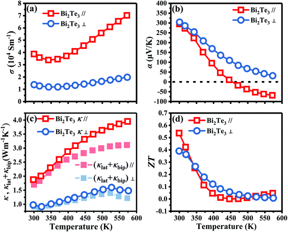
As shown in Fig. 5c, κ∥ and κ⊥ at 300 K are 1.88 and 0.98 W m−1 K−1, respectively. The solid points in Fig. 5c indicate that the sum of lattice thermal conductivity (κlat) and bipolar thermal conductivity (κbip) makes a significant contribution to the total κ. Owing to the dominance of electrical properties rather than the thermal properties, a highest ZT∥ 0.54 is obtained at 300 K as shown in Fig. 5d. The unsatisfactory ZT mainly attributes to the low σ deriving from the inferior n, and also a high κ. Therefore, further research on optimizing of n by increasing antisite defects was conducted through adjusting the Te content, which is a simple and effective approach. On the other hand, the increased point defects can enhance the scattering of phonons and reduce κ. A higher TE performance is expected to obtain by simply adjusting the amount of Te. Hereafter, a series of p-type Bi2Te3−x (x = 0, 0.02, 0.04, 0.06, 0.08) bulks were prepared by TGGM and the TE transport properties of in-plane with a subscript of ∥ will be discussed.
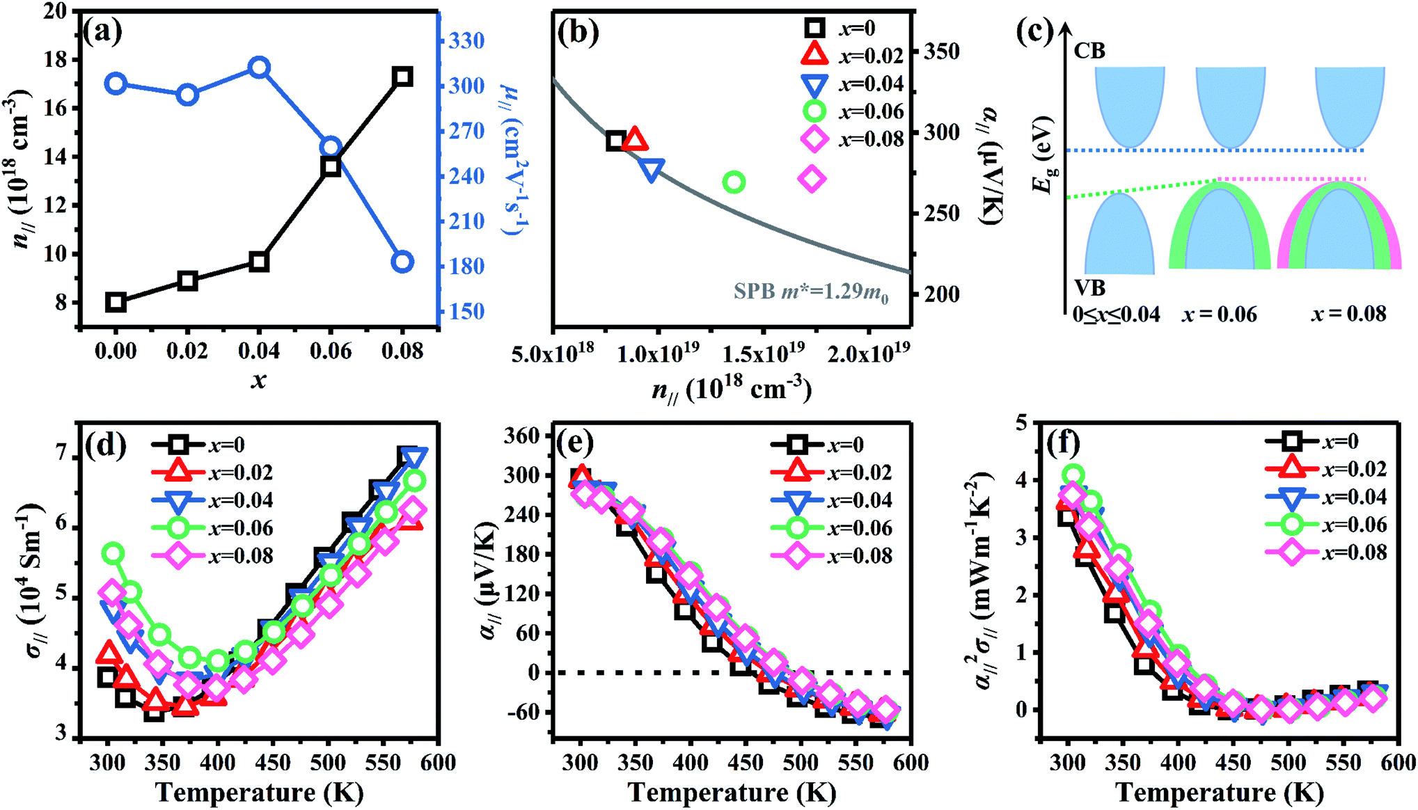
Fig. 6 shows the electrical transport properties for Bi2Te3−x (x = 0, 0.02, 0.04, 0.06, 0.08) single crystals along the in-plane. The n∥ and μ∥ in Fig. 6a show an inverse variation. The n∥ of x = 0 bulk is 8.01 × 1018 cm−3 and slowly increases to 8.89 × 1018 cm−3 (x = 0.02) and 9.68 × 1018 cm−3 (x = 0.04). When the amount of Te is further reduced, the n∥ is significantly enhanced to 1.36 × 1019 cm−3 (x = 0.06) and 1.73 × 1019 cm−3 (x = 0.08). The μ∥ is ca. 294.32–312.53 cm2 V−1 s−1 at 0 ≤ x ≤ 0.04 and decreases to 259.40 cm2 V−1 s−1 (x = 0.06) and 183.28 cm2 V−1 s−1 (x = 0.08). The reduction of μ∥ may be caused by the change of effective masses (m*) as expressed in eqn (7):2
| |
 | (7) |
where
e is the electron charge and
τ is the carrier scattering time.
Eqn (7) indicates that an enhanced
m* will result in a reduced
μ. What's more,
m* can be simply estimated by the Pisarenko relationship between
α and
n based on the single parabolic band (SPB) model according to
eqn (8):
71| |
 | (8) |
where
kB is the Boltzmann constant and
h is the Planck constant. On the basis of
eqn (8), the
α is proportional to
m* and inversely to
n. As shown in
Fig. 6b, the theoretical Pisarenko curve with
m* of 1.29
m0 and the experimental data at room temperature are depicted by the gray line and marks, respectively. The experimental data at 0 ≤
x ≤ 0.04 agree every well with the theoretical Pisarenko curve and follow a SPB behavior. The reduced
α∥ of 0 ≤
x ≤ 0.06 bulks in
Fig. 6b at 300 K is dominated by the significantly increased
n∥ rather than the variated
m* (
x = 0.06). Although the
n∥ is enhanced at
x = 0.08, the
α∥ holds a similar value with
x = 0.06 due to the further increased
m*. According to PDOS in
Fig. 1e and f, Te atoms contribute most near the VBM and the large lack of Te (0.06 ≤
x ≤ 0.08) in this work may play as a dopant and cause the change of band structure which could increase
m*. The
Eg is also estimated using the maximum Seebeck coefficient (
αmax) and the corresponding temperature (
T) as shown in
eqn (9):
71,72
 |
| | Fig. 6 Electrical transport properties for Bi2Te3−x (x = 0, 0.02, 0.04, 0.06, 0.08) single crystal along the in-plane. (a) Carrier concentration (n∥) and mobility (μ∥), (b) dependence between the α∥ and n∥ (the Pisarenko curve) at 300 K, (c) schematic representation of the band structure, (d) electrical conductivity (σ∥), (e) Seebeck coefficient (α∥), and (f) power factor (α∥2σ∥). | |
The calculated Eg is ca. 0.17 eV for 0 ≤ x ≤ 0.04 and reduces to 0.16 eV for 0.06 ≤ x ≤ 0.08, resulting an increased n. The schematic of the variation for band structure and Eg is shown in Fig. 6c. The widened valence band and narrowed Eg can enhance the m* and n, respectively, as shown in Fig. 6a and b σ∥ of all bulks shows a similar temperature dependence as increasing temperature in Fig. 6d. The σ∥ increases from 3.87 × 10⁴ S m−1 (x = 0) to 5.64 × 10⁴ S m−1 (x = 0.06) and then decreases to 5.08 × 10⁴ S m−1 (x = 0.08) at 300 K, which is the results of the combination of n∥ and μ∥ according to σ = neμ. All bulks in Fig. 6e have a positive α∥ at room temperature indicating a p-type semi-conductive behavior, but show a transformation from p-type to n-type between 400 K and 500 K. As increasing x, α∥ decreases from 294.89 μV K−1 at x = 0 to 269.30 μV K−1 at x = 0.06 due to the significantly increased n∥ in Fig. 6a. Owing to the high σ∥ (5.64 × 10⁴ S m−1) and α∥ (269.30 μV K−1), a maximum PF∥ 4.09 mW m−1 K−2 is obtained at 300 K for x = 0.06 as shown in Fig. 6f, which has an enhancement of 21% compared with the intrinsic Bi2Te3 at the same temperature.
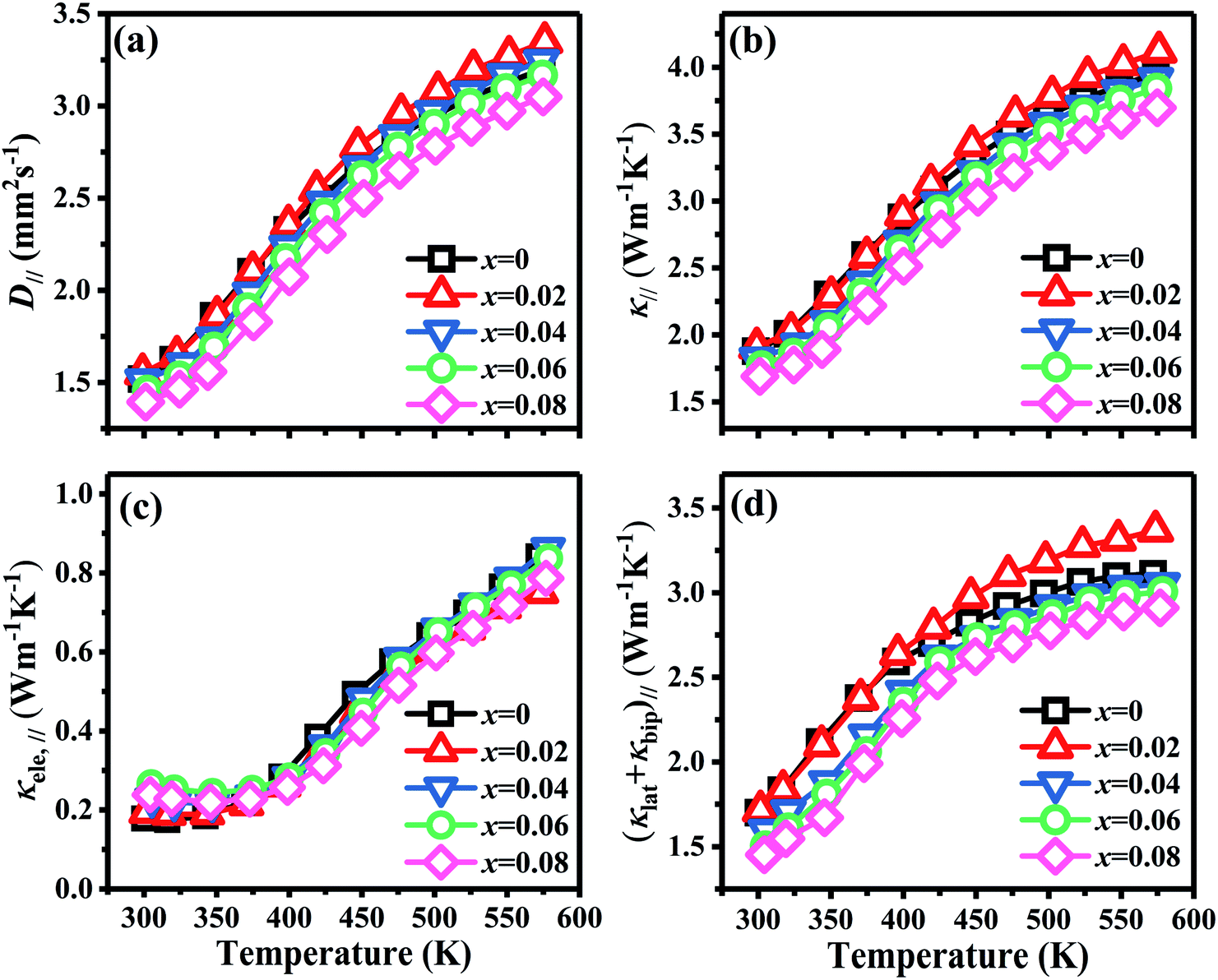
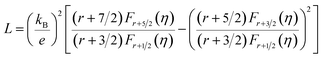
Fig. 7 shows the temperature dependence of thermal transport properties for Bi2Te3−x (x = 0, 0.02, 0.04, 0.06, 0.08) single crystals along the in-plane. The thermal diffusivity (D∥) of all bulks monotonously increases as increasing the temperature from 300 K to 573 K in Fig. 7a. D∥ decreases from 1.52 mm2 s−1 for x = 0 to 1.39 mm2 s−1 for x = 0.08 at 300 K. κ∥ of all bulks in Fig. 7b presents the similar varying trend with D∥ as increasing the temperature. κ is the sum of the κele (electronic thermal conductivity), the κlat (lattice thermal conductivity) and the κbip (bipolar thermal conductivity). And κele can be estimated by the Wiedemann–Franz relation: κele = LσT, where L is the Lorenz number, T is the absolute temperature, respectively. The L can be calculated basing on SPB model using eqn (10)–(12):50
| |
 | (10) |
| |
 | (11) |
| |
 | (12) |
where
r,
Fn(
η) and
η are the scattering parameter, the Fermi integral and reduced Fermi energy, respectively. The varying trend of calculated
κele, ∥ in
Fig. 7c is similar to that of
σ∥ (
Fig. 6d). The highest
κele, ∥ is 0.86 W m
−1 K
−1 for
x = 0.04 at 573 K, while the lowest (
κlat +
κbip)
∥ is 1.45 W m
−1 K
−1 obtained at
x = 0.08 at 300 K, indicating that (
κlat +
κbip)
∥ plays a dominant role in thermal transport properties for all bulks. (
κlat +
κbip)
∥ decreases from 1.70 W m
−1 K
−1 to 1.45 W m
−1 K
−1 as
x increasing from 0 to 0.08 as shown in
Fig. 7d. The reduction of (
κlat +
κbip)
∥ is attributed to the enhancement of point defects which can enhance the scattering of phonons.
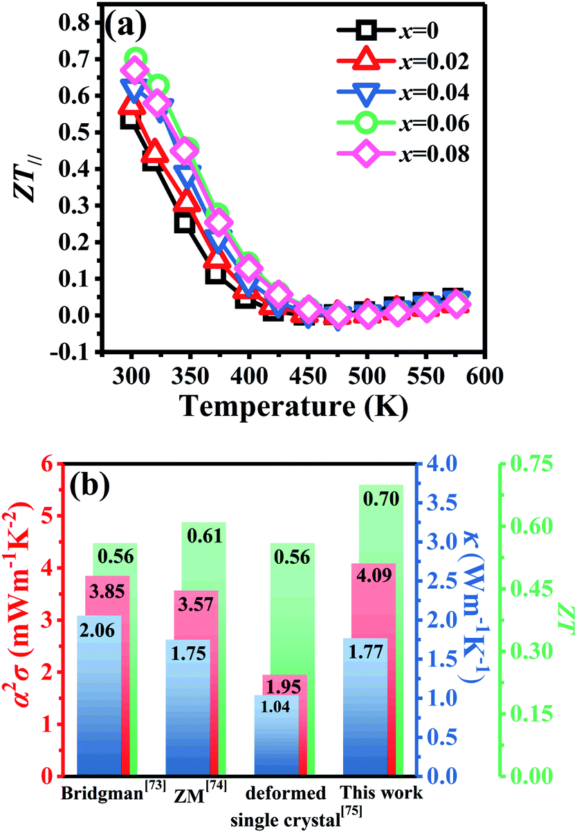
Fig. 8a shows the temperature dependence of
ZT∥ for Bi
2Te
3−x (
x = 0, 0.02, 0.04, 0.06, 0.08) single crystals along the in-plane. The deteriorated
α∥ results in a reduction of
ZT∥ with increasing temperature. However, owing to the high PF
∥ in
Fig. 6f and low
κ∥ in
Fig. 7b, the
x = 0.06 bulk attains the highest
ZT∥ value of 0.70 at 300 K, which is 30% higher than that (0.54) of the intrinsic Bi
2Te
3, indicating that producing point defects is effective to enhance the TE properties of Bi
2Te
3 single crystals.
Fig. 8b shows a comparison of the TE properties at 300 K for p-type Bi
2Te
3-based bulks prepared by different methods. The result shows that the TE properties of Bi
2Te
3 single crystals prepared by TGGM described in this work is comparable with other early reported values.
73–75 This result indicates that TGGM is a simple and effective method to prepare Bi
2Te
3-based single crystals.
 |
| | Fig. 7 Temperature dependence of thermal transport properties for Bi2Te3−x (x = 0, 0.02, 0.04, 0.06, 0.08) single crystal along the in-plane. (a) Thermal diffusivity (D∥), (b) total thermal conductivity (κ∥), (c) electronic thermal conductivity (κele, ∥), and (d) the sum of lattice thermal conductivity and bipolar thermal conductivity ((κlat + κbip)∥). | |
 |
| | Fig. 8 (a) Temperature dependence of figure of merit (ZT∥) for Bi2Te3−x (x = 0, 0.02, 0.04, 0.06, 0.08) single crystals along the in-plane and (b) comparison of TE properties with early reports. | |
4. Conclusions
In Bi2Te3 single crystals, the calculated electronic structure indicates that Te atoms play a dominant role near valence band maxima (VBM), whereby the change of Te atoms may broaden the band structure and enhance m*. The calculated formation energy under the Te-lack condition indicates that Bi can easily enter into Te-sites to form antisite defects and provide holes. The effects of point defects on TE properties were investigated detailedly by preparing a series of p-type Bi2Te3−x (x = 0, 0.02, 0.04, 0.06, 0.08) single crystals via TGGM. The lack of Te increases antisite defects and broadens the band structure which can increase n∥ and m*, respectively, apart from an increased PF∥ 4.09 mW m−1 K−2 for x = 0.06 composition, also contributing the lowest κ∥ 1.69 W m−1 K−1 at x = 0.08 achieved by the increased scattering of phonons. Owing to the simultaneous optimization of electrical transport properties and thermal conductivity, a highest ZT∥ 0.70 was obtained for x = 0.06 composition at 300 K, which is 30% higher than that (0.54) of the intrinsic Bi2Te3.
Conflicts of interest
There are no conflicts to declare.
Acknowledgements
This work was supported by National Key Research and Development Program of China (Grant No. 2018YFB0703600) and the National Natural Science Foundation of China (Grant No. 11474176).
Notes and references
- L. E. Bell, Science, 2008, 321, 1457–1461 CrossRef CAS PubMed.
- F. J. Disalvo, Science, 1999, 285, 703–706 CrossRef CAS PubMed.
- S. B. Riffat and X. Ma, Appl. Therm. Eng., 2003, 23, 913–935 CrossRef.
- H. J. Goldsmid, Introduction to Thermoelectricity, Springer Series in Materials Science, Verlag Berlin Heidelberg, 2010 Search PubMed.
- H. J. Goldsmid, Thermoelectric refrigeration, Springer, 2013 Search PubMed.
- J. Pei, L. J. Zhang, B. P. Zhang, P. P. Shang and Y. C. Liu, J. Mater. Chem. C, 2017, 5, 12492–12499 RSC.
- Y. Pei, A. D. Lalonde, N. A. Heinz, X. Shi, S. Iwanaga, H. Wang, L. Chen and G. J. Snyder, Adv. Mater., 2011, 23, 5674–5678 CrossRef CAS PubMed.
- J. P. Heremans, V. Jovovic, E. S. Toberer, A. Saramat, K. Kurosaki, A. Charoenphakdee, S. Yamanaka and G. J. Snyder, Science, 2008, 321, 554–557 CrossRef CAS PubMed.
- J. P. Heremans, B. Wiendlocha and A. M. Chamoire, Energy Environ. Sci., 2012, 5, 5510–5530 RSC.
- Y. Pei, X. Shi, A. Lalonde, H. Wang, L. Chen and G. J. Snyder, Nature, 2011, 473, 66–69 CrossRef CAS PubMed.
- L. Zheng, W. Li, S. Lin, J. Li, Z. Chen and Y. Pei, ACS Energy Lett., 2017, 2, 563–568 CrossRef CAS.
- W. Li, L. Zheng, B. Ge, S. Lin, X. Zhang, Z. Chen, Y. Chang and Y. Pei, Adv. Mater., 2017, 29, 1605887 CrossRef PubMed.
- J. F. Li, W. S. Liu, L. D. Zhao and M. Zhou, NPG Asia Mater., 2012, 2, 152–158 CrossRef.
- X. Su, P. Wei, H. Li, W. Liu, Y. Yan, P. Li, C. Su, C. Xie, W. Zhao, P. Zhai, Q. Zhang, X. Tang and C. Uher, Adv. Mater., 2017, 29, 1602013 CrossRef PubMed.
- W. Kim, J. Zide, A. Gossard, D. Klenov, S. Stemmer, A. Shakouri and A. Majumdar, Phys. Rev. Lett., 2006, 96, 045901 CrossRef PubMed.
- W. M. Yim and F. D. Rosi, Solid-State Electron., 1972, 15, 1121–1140 CrossRef CAS.
- M. Hong, Z. G. Chen and J. Zou, Chin. Phys. B, 2018, 27, 048403 CrossRef.
- S. Nakajima, J. Phys. Chem. Solids, 1963, 24, 479–485 CrossRef CAS.
- Z. Johan, P. Picot and F. Ruhlmann, Can. Mineral., 1987, 25, 625–638 CAS.
- B. L. Huang and M. Kaviany, Phys. Rev. B: Condens. Matter Mater. Phys., 2008, 77, 125209 CrossRef.
- H. J. Goldsmid and R. W. Douglas, Br. J. Appl. Phys., 1954, 5, 386–390 CrossRef.
- Y. Pan, T. R. Wei, C. F. Wu and J. F. Li, J. Mater. Chem. C, 2015, 3, 10583–10589 RSC.
- T. Zhu, L. Hu, X. Zhao and J. He, Adv. Sci., 2016, 3, 1600004 CrossRef PubMed.
- L. Hu, T. Zhu, X. Liu and X. Zhao, Adv. Funct. Mater., 2014, 24, 5211–5218 CrossRef CAS.
- J. J. Shen, L. P. Hu, T. J. Zhu and X. B. Zhao, Appl. Phys. Lett., 2011, 99, 124102 CrossRef.
- Y. Pan and J. F. Li, NPG Asia Mater., 2016, 8, e275 CrossRef CAS.
- R. Zhai, L. Hu, H. Wu, Z. Xu, T. J. Zhu and X. B. Zhao, ACS Appl. Mater. Interfaces, 2017, 9, 28577–28585 CrossRef CAS PubMed.
- S. I. Kim, K. H. Lee, H. A. Mun, H. S. Kim, S. W. Hwang, J. W. Roh, D. J. Yang, W. H. Shin, X. S. Li, Y. H. Lee, G. J. Snyder and S. W. Kim, Science, 2015, 348, 109–114 CrossRef CAS PubMed.
- B. Poudel, Q. Hao, Y. Ma, Y. Lan, A. Minnich, B. Yu, X. Yan, D. Wang, A. Muto, D. Vashaee, X. Chen, J. Liu, M. S. Dresselhaus, G. Chen and Z. Ren, Science, 2008, 320, 634–638 CrossRef CAS PubMed.
- Y. Ma, Q. Hao, B. Poudel, Y. Lan, B. Yu, D. Wang, G. Chen and Z. Ren, Nano Lett., 2008, 8, 2580–2584 CrossRef CAS PubMed.
- Y. Zheng, Q. Zhang, X. Su, H. Xie, S. Shu, T. Chen, G. Tan, Y. Yan, X. Tang, C. Uher and G. J. Snyder, Adv. Energy Mater., 2015, 5, 1401391 CrossRef.
- A. Soni, Z. Yanyuan, Y. Ligen, M. K. K. Aik, M. S. Dresselhaus and Q. Xiong, Nano Lett., 2012, 12, 1203–1209 CrossRef CAS PubMed.
- H. W. Jeon, H. P. Ha, D. B. Hyun and J. D. Shim, J. Phys. Chem. Solids, 1991, 52, 579–585 CrossRef CAS.
- H. J. Goldsmid, Proc. Phys. Soc., 1958, 71, 633–646 CrossRef CAS.
- T. Plecháček, J. Navrátil, J. Horák and P. Lošt’ák, Philos. Mag., 2004, 84, 2217–2228 CrossRef.
- S. K. Feng, S. M. Li and H. Z. Fu, Chin. Phys. B, 2014, 23, 117202 CrossRef.
- B. Jariwala, D. Shah and N. M. Ravindra, J. Electron. Mater., 2015, 44, 1509–1516 CrossRef CAS.
- D. Liu, X. Li, P. M. Borlido, S. Botti, R. Schmechel and M. Rettenmayr, Sci. Rep., 2017, 7, 43611 CrossRef PubMed.
- A. T. Duong, V. Q. Nguyen, G. Duvjir, V. T. Duong, S. Kwon, J. Y. Song, J. K. Lee, J. E. Lee, S. Park, T. Min, J. Lee, J. Kim and S. Cho, Nat. Commun., 2016, 7, 13713 CrossRef CAS PubMed.
- J. Choi, S. Choi, J. Choi, Y. Park, H.-M. Park, H. W. Lee, B. C. Woo and S. Cho, Phys. Status Solidi B, 2004, 241, 1541–1544 CrossRef CAS.
- D. A. Tuan, J. Choi, Y. Shin, S. Cho, H. M. Park, W. Kim, C. Hwang and D. D. Dung, J. Korean Phys. Soc., 2012, 61, 1675–1678 CrossRef CAS.
- G. K. H. Madsen, J. Carrete and M. J. Verstraete, Comput. Phys. Commun., 2018, 231, 140–145 CrossRef CAS.
- G. Kresse and J. Furthmuller, Phys. Rev. B: Condens. Matter Mater. Phys., 1996, 54(16), 11169–11186 CrossRef CAS.
- G. Kresse and J. Furthmüller, Comput. Mater. Sci., 1996, 6, 15–50 CrossRef CAS.
- J. P. Perdew, K. Burke and M. Ernzerhof, Phys. Rev. Lett., 1996, 77, 3865 CrossRef CAS PubMed.
- P. E. Blöchl, Phys. Rev. B: Condens. Matter Mater. Phys., 1994, 50, 17953 CrossRef.
- S. Grimme, J. Antony, S. Ehrlich and S. Krieg, J. Chem. Phys., 2010, 132, 154104 CrossRef PubMed.
- S. Grimme, S. Ehrlich and L. Goerigk, J. Comput. Chem., 2011, 32, 1456–1465 CrossRef CAS PubMed.
- W. Setyawan and S. Curtarolo, Comput. Mater. Sci., 2010, 49, 299–312 CrossRef.
- D. M. Rowe, CRC Handbook of Thermoelectrics, CRC Press, 1995 Search PubMed.
- K. Peng, B. Zhang, H. Wu, X. Cao, A. Li, D. Yang, X. Lu, G. Wang, X. Han, C. Uher and X. Zhou, Mater. Today, 2018, 21, 501–507 CrossRef CAS.
- C. G. Van De Walle and J. Neugebauer, J. Appl. Phys., 2004, 95, 3851–3879 CrossRef CAS.
- A. Hashibon and C. Elsässer, Phys. Rev. B: Condens. Matter Mater. Phys., 2011, 84, 144117 CrossRef.
- J. M. Zhang, W. Ming, Z. Huang, G. B. Liu, X. Kou, Y. Fan, K. L. Wang and Y. Yao, Phys. Rev. B: Condens. Matter Mater. Phys., 2013, 88, 235131 CrossRef.
- D. West, Y. Y. Sun, H. Wang, J. Bang and S. B. Zhang, Phys. Rev. B: Condens. Matter Mater. Phys., 2012, 86, 121201 CrossRef.
- T. J. Scheidemantel, C. Ambrosch-Draxl, T. Thonhauser, J. V. Badding and J. O. Sofo, Phys. Rev. B: Condens. Matter Mater. Phys., 2003, 68, 125210 CrossRef.
- P. Larson, Phys. Rev. B: Condens. Matter Mater. Phys., 2003, 68, 155121 CrossRef.
- I. G. Austin, Proc. Phys. Soc., 1958, 72, 545–552 CrossRef CAS.
- J. Black, E. M. Conwell, L. Seigle and C. W. Spencer, J. Phys. Chem. Solids, 1957, 2, 240–251 CrossRef CAS.
- T. Inamoto and M. Takashiri, J. Appl. Phys., 2016, 120, 125105 CrossRef.
- S. J. Youn and A. J. Freeman, Phys. Rev. B: Condens. Matter Mater. Phys., 2001, 63, 085112 CrossRef.
- B. Ryu and M. W. Oh, J. Korean Ceram. Soc., 2016, 53, 273–281 CrossRef CAS.
- S. K. Mishra, S. Satpathy and O. Jepsen, J. Phys.: Condens. Matter, 1997, 9, 461–470 CrossRef CAS.
- B. Ryu, B. S. Kim, J. E. Lee, S. Joo, B. Min, H. W. Lee and S. Park, J. Korean Phys. Soc., 2016, 68, 115–120 CrossRef CAS.
- P. Larson, S. D. Mahanti and M. G. Kanatzidis, Phys. Rev. B: Condens. Matter Mater. Phys., 2000, 61, 8162–8171 CrossRef CAS.
- N. F. Hinsche, B. Y. Yavorsky, I. Mertig and P. Zhan, Phys. Rev. B: Condens. Matter Mater. Phys., 2011, 84, 165214 CrossRef.
- M. W. Oh, J. H. Son, B. S. Kim, S. D. Park, B. K. Min and H. W. Lee, J. Appl. Phys., 2014, 115, 133706 CrossRef.
- Y. Liu, J. Chen, H. Deng, G. Hu, D. Zhu and N. Dai, Sci. Rep., 2016, 6, 32661 CrossRef CAS PubMed.
- M. Situmorang, Phys. Status Solidi B, 1986, 134, K83–K88 CrossRef CAS.
- J. H. Dennis, Adv. Energy Convers., 1961, 1, 99–105 CrossRef CAS.
- A. F. May and G. J. Snyder, in Introduction to Modeling Thermoelectric Transport at High Temperatures in Thermoelectrics and its Energy Harvesting, ed. D. M. Rowe, CRC Press, 2012 Search PubMed.
- D. Guo, C. Hu and C. Zhang, Mater. Res. Bull., 2013, 48, 1984–1988 CrossRef CAS.
- H. Chi, W. Liu, K. Sun, X. Su, G. Wang, P. Lošt'ák, V. Kucek, Č. Drašar and C. Uher, Phys. Rev. B: Condens. Matter Mater. Phys., 2013, 88, 045202 CrossRef.
- C. W. Hwang, D. B. Hyun, H. P. Ha and T. S. Oh, J. Mater. Sci., 2001, 36, 3291–3297 CrossRef CAS.
- S. Grasso, N. Tsujii, Q. Jiang, J. Khaliq, S. Maruyama, M. Miranda, K. Simpson, T. Mori and M. J. Reece, J. Mater. Chem. C, 2013, 1, 2362–2367 RSC.
Footnote |
| † Electronic supplementary information (ESI) available. See DOI: 10.1039/c9ra01738k |
|
| This journal is © The Royal Society of Chemistry 2019 |
Click here to see how this site uses Cookies. View our privacy policy here. 
 Open Access Article
 This Open Access Article is licensed under a Creative Commons Attribution-Non Commercial 3.0 Unported Licence
 *a,
Peng-Peng Shangb,
Zhihang Shana,
Zhiyue Zhanga,
Haiyun Gua and
Kaibin Wena
*a,
Peng-Peng Shangb,
Zhihang Shana,
Zhiyue Zhanga,
Haiyun Gua and
Kaibin Wena
 ,
,  and
and  of holes along different principal axes were calculated as defined in eqn (1):50,51

 ,
,  and
and  of holes along the different principal axes were calculated to be 0.31 m0, 0.04 m0 and 0.04 m0, respectively, indicating that the TE properties of p-Bi2Te3 may be anisotropic.

 and extra holes (h˙), causing a large decrement of lattice constants for Bi2Te3. The volatilization of Te can generate positively charged vacancy
  and extra electrons (e′) as described in eqn (4). The formation of
  is easier than
  during the sintering process because of the lower energy of evaporation for Te (52.55 kJ mol−1) compared with Bi (104.80 kJ mol−1). So, eqn (4) plays a dominant role, which is coincided quite well with the calculation of formation energy in Table 1. However, the close electronegativity between Bi (2.02) and Te (2.01) makes it easy for Bi to jump to the Te-sites, forming antisite defects along with h˙ generated as shown in eqn (5). What's more,
  and
and  can cancel each other out with a ratio of 2
 and fix h˙ as described in eqn (6) and enlarge the lattice of Bi2Te3 as shown in Fig. 4b. With the further lack of Te, the effect of eqn (5) is enhanced while the function of eqn (6) is limited, resulting in the shrinkage of Bi2Te3 lattice in Fig. 4b and the enhancement of n∥ in Fig. 6a. According to the above analysis, the point defect Bi_Te plays a dominant role in all Bi2Te3 bulks and leads to the decrease of lattice constant c as shown in Table 3, which is corresponding to the reduction of lattice constant c from DFT calculation as shown in Table 2.