
 Open Access Article
 This Open Access Article is licensed under a
 Creative Commons Attribution 3.0 Unported Licence
The energy band structure analysis and 2 μm Q-switched laser application of layered rhenium diselenide
Yongping Yao†
b,
Xiaowen Li†c,
Rengang Songab,
Na Cuib,
Shande Liu *ab,
Huiyun Zhangb,
Dehua Lib,
Qiangguo Wangb,
Yan Xu*ab and
Jingliang Hed
*ab,
Huiyun Zhangb,
Dehua Lib,
Qiangguo Wangb,
Yan Xu*ab and
Jingliang Hed
aCollege of Electrical, Engineering and Automation, Shandong University of Science and Technology, Qingdao, 266590, China. E-mail: pepsl_liu@163.com; x1y5@163.com
bCollege of Electronic and Information Engineering, Shandong University of Science and Technology, Qingdao 266590, China
cKey Laboratory of Micro-nano Measurement-Manipulation and Physics, Ministry of Education, Department of Applied Physics, Beihang University, Beijing 100191, China
dState Key Laboratory of Crystal Materials, Shandong University, Jinan 250100, China
First published on 8th May 2019
Abstract
Layered rhenium diselenide (ReSe2) has triggered strong interest because of its outstanding optical and electrical properties. In this paper, we prepared a high-quality multilayer ReSe2 saturable absorber with a liquid-phase exfoliation method and characterized its saturable absorption properties around 2 μm. During the Q-switching regime, a maximum average output power of 1.7 W was obtained. A shortest pulse width of 925.8 ns was measured and the corresponding single pulse energy and peak power were 17.6 μJ and 19.0 W, respectively. The results indicate that layered ReSe2 is a promising alternative as a nonlinear optical modulator near the 2 μm region.
1. Introduction
Short laser pulses, especially in the eye-safe range of 2 μm,1 have constituted an active research topic in recent years because of their wide variety of applications in the fields of atmospheric gas analysis,2 wind lidar,3 laser surgery,4 and so on. Passive Q-switching (PQS) and mode-locking lasers are the essential technology for generating short laser pulses with pulse width ranging from the nanosecond to femtosecond timescale. In such passive Q-switching lasers, the saturable absorber (SA) is the key element and thus the characteristics of output laser beams strongly depend on the nature of the SA materials. Up to now, semiconductor saturable absorber mirrors (SESAMs),5 Cr:ZnS6, Cr:ZnSe7, carbon nanomaterials,8,9 topological insulators (TI)10,11 and black phosphorus (BP),12 have been recognized as reliable SAs for 2 μm lasers. However, the utilization of SESAMs is restricted by reasons of the complicated and expensive fabrication process as well as narrow absorption bandwidth. The Cr-doped crystals, like Cr:ZnS and Cr:ZnSe, have played pivotal roles at 2 μm region lately.13 Nevertheless, the lack of quality and high-cost are the key factor which constrain them further development. The extraordinary performances such as high carrier mobility, easy-preparation, cost-effective, remarkable electrical and thermal conductivity make the graphene attractive candidate as SAs during the PQS regime. But the low absorption efficiency may limit its applications. Hence, more efforts should be made to explore novel nonlinear optical materials for SAs in the 2 μm region.Owing to possessing excellent saturable absorption properties and environmental stability, transition metal dichalcogenides (TMDs), which have layered structure of the X–M–X form (where M denotes a transition metal and X denotes a chalcogen), have been achieved encouraging results at 2–3 μm laser operations.14–19 Rhenium diselenide (ReSe2), one of the relatively unexplored members of the TMDs family, has attracted a significant attention because of its unusual electronic and optical behaviors.20–24 It crystallizes in a distorted octahedral (1T) diamond-chain structure at the triclinic symmetry. It demonstrates anisotropic response arising from its in-plane anisotropic structure. Rhenium atom contain an extra electron in the d-orbitals,25,26 which is different from other 2H phase TMDs (e.g., MoS2, WS2). ReSe2 films can be easily exfoliated from its bulk crystal because of the relatively weaker van der Waals forces between interlayers. The recovery time of ReSe2 on the order of 10 ps, which is beneficial for the ultrafast pulse generation. In addition, the layered ReSe2 samples show no obvious signs of degradation while exposed to exterior circumstance for several weeks in our study. All the characteristics mentioned above indicate that the layered ReSe2 is an excellent material for nonlinear optical modulate and it has been applied as SA at 1–2 μm regions.27–29 In 2019, Li et al. reported a ReSe2 Q-switched Tm:YLF laser, however, the laser pulse width and pulse repetition rate were only 1.61 μs and 28.78 kHz, respectively.29 According to excellent properties of the ReSe2 material, the laser pulse characteristics at 2 μm would be further improved.
In this paper, a high-quality large-area multilayer ReSe2 SA was successfully prepared and the saturable absorption properties at 2 μm region were investigated by the open-aperture Z-scan method. Based on ReSe2 as SA, a stable all-solid-state Q-switched Tm:YAP crystal laser was realized. Under an absorbed pump power of 8.5 W, a continuous-wave (CW) output power of 2.9 W was generated, corresponding to a slope efficiency of 44%. In the ReSe2 Q-switching regime, a maximum average output power of 1.7 W was obtained, giving a slope efficiency of 37%. The shortest pulse duration of 925.8 ns was generated at a repetition rate of 89.4 kHz, resulting in the maximum single pulse energy and peak power of 17.6 μJ and 19.0 W, respectively.
2. Theoretical analysis of the energy band structure
A monolayer supercell of ReSe2 with 16 Re atoms and 32 Se atoms and the same structures with one and two Se atomic vacancies are constructed. The ratios (R) between Re and Se atoms for the three structures are 1![[thin space (1/6-em)]](https://www.rsc.org/images/entities/char_2009.gif) :2, 1:1.937 and 1:1.875. The first principle calculation of band structure is based on the Vienna ab initio simulation package (VASP).30 The Perdew–Burke–Ernzerhof (PBE) functional within the generalized gradient approximation (GGA) is adopted to account for the exchange and correlation part.31 A plane wave basis set with an energy cutoff of 550 eV and the PAW pseudopotential implemented in VASP are applied. The Brillouin zone is sampled by a Monkhorst–Pack k-point mesh of 21 × 21 × 1. In order to avoid the interactions among ReSe2 layers, the vacuum space thickness along the c axis is set to 20 Å.
:2, 1:1.937 and 1:1.875. The first principle calculation of band structure is based on the Vienna ab initio simulation package (VASP).30 The Perdew–Burke–Ernzerhof (PBE) functional within the generalized gradient approximation (GGA) is adopted to account for the exchange and correlation part.31 A plane wave basis set with an energy cutoff of 550 eV and the PAW pseudopotential implemented in VASP are applied. The Brillouin zone is sampled by a Monkhorst–Pack k-point mesh of 21 × 21 × 1. In order to avoid the interactions among ReSe2 layers, the vacuum space thickness along the c axis is set to 20 Å.
The calculated band structures corresponding to the atomic structures mentioned above are shown in Fig. 1(a–c) respectively. From Fig. 1(a), it can be seen that the monolayer supercell ReSe2 with no vacancy has a bandgap of ∼1.22 eV, which is in good agreement with previous calculations of ReSe2.25 While in Fig. 1(b) and (c), the bandgaps of the structures with one and two Se atomic vacancies are ∼0.75 eV and ∼0.50 eV respectively. With the increase of Se atomic vacancies, the bandgap of monolayer ReSe2 decreases from 1.22 eV to 0.50 eV, mainly due to the reconstruction of atoms around the vacancies perturbs the periodic potential. The corresponding absorption wavelength edge for the structures mentioned above extends from 1 μm to 2.48 μm. To identify the existence of the vacancies in the ReSe2 sample, the energy-dispersive X-ray spectroscopy (EDS) was measured. Fig. 2(a) presents the ratio of Re to Se was 1.877, which confirmed that some Se vacancies existed in the ReSe2 sample.
 | ||
| Fig. 1 Theoretical band structures for (a) R = 1:2, (b) R = 1:1.937, and (c) R = 1:1.875. | ||
 | ||
| Fig. 2 (a) EDS image and the corresponding Re to Se radio of the ReSe2 sample, (b) fabrication process of ReSe2-SA. | ||
These calculation results of monolayer ReSe2 are analogous to that of monolayer ReS2 as in ref. 18. Moreover, the bandgap of certain ReSe2 configuration is smaller than that of ReS2 with the same vacancy concentration which mainly attribute to the distortion of Re–Se bond is larger than that of Re–S bond. It can be concluded that the introduction of Se vacancies in monolayer ReSe2 makes it a promising candidate as a broad band saturable absorber.
3. Fabrication and optical characteristics of the ReSe2-SA
As shown in Fig. 2(b), the ReSe2-SA was prepared with LPE method, which has been extensively applied in BP and other 2D materials17–19,32 fabrication. This method enables large-scale exfoliation and uniform dispersion in the exfoliation medium. First, the bulk ReSe2 with purity of 99.995%, purchased from HQ Graphene Inc, was ground to powder in a mortar. Then, the ReSe2 powder was dispersed into ethyl alcohol followed by 4 hours sonication. To avoid feature changes of the ReSe2 under high temperature, the ultrasonic process was operated at a suitable interval and ice was added during the ultrasonic process. After that, the as-prepared ReSe2 solution was centrifuged at 4000 rpm for 10 min with the aim of removing the large-size ReSe2 sheets and the supernatant was collected for standby. Finally, the processed ReSe2 solution was spin coated on an output mirror (T = 5% @ 1.9–2.1 μm), and dried under an infrared oven lamp.In order to investigate the thickness and distribution of the ReSe2 flakes, the atomic force microscopy (AFM, Veeco Dimension Icon) was employed to study the morphology of the as-prepared ReSe2-SA. Fig. 3(a) shows an AFM scan image of the sample in a large area, because of the weak interlayer coupling of the ReSe2. The average thickness of the transferred layers on the treated SAM is approximately 10 nm, as presented in Fig. 3(b), corresponding to the layer number of ∼14 since the height of monolayer ReSe2 is 0.7 nm.24 The Raman spectra of ReSe2-SA was measured by a Raman microscope with a 532 nm laser as the excitation source, as shown in Fig. 3(c). Due to the weak lattice coupling between the layers, these vibrational intense of the low-frequency modes are stronger and the low-frequency modes are easier to be observed. Three typical Raman peaks at 119 cm−1, 161 cm−1 and 174 cm−1, respectively, were observed, which is consistent with the previous reported results.22,27,29
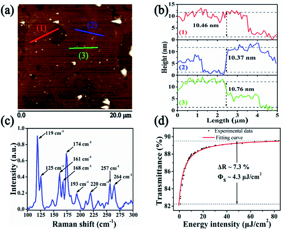 | ||
| Fig. 3 (a) AFM image of ReSe2-SA, (b) height variations, (c) Raman spectra of the ReSe2-SA, and (d) nonlinear transmission versus energy intensity. | ||
The saturable absorption properties of ReSe2-SA were also characterized with an open aperture Z-scan method based on a home-made SESAM mode-locked 3 ps Tm:YAP laser at 1940 nm with a repetition rate of 92.5 MHz. The transmittances of the ReSe2-SA at different incident fluences were measured and fitted by the following formula:
| T(F) = Aexp(−ΔT/(1 + F/Fsat) + αns) | (1) |
4. Experimental
To investigate the saturable absorption properties of ReSe2 in 2 μm region, a compact concave-plano cavity with a length of 24 mm was employed, and the experimental setup is shown in Fig. 4. An high quality a-cut Tm:YAP crystal with both sides high-transmission (HT) coated at 793 nm and 1980 nm was employed as the gain medium. The pump source was a 793 nm fiber coupled LD with a core diameter of 200 μm and a numerical aperture (N.A.) of 0.22. The pump beam was collimated into the Tm:YAP crystal with a spot radius of 100 μm through a 1:1 focusing system. The mirror M1 was a concave mirror with a curvature radius of 300 mm coated for anti-reflection (AR) at 780–810 nm on the entrance surface, and high-reflectivity (HR) at 1.9–2.1 μm on the cavity surface. The output coupler M2 was a flat mirror with a transmission of 5% at around 2 μm. On behalf of removing the heat, the Tm:YAP crystal was wrapped with an indium foil and mounted in a copper block sustained at 17 °C by circulating water. In the measurement of laser output power, a dichroic beamsplitter was applied to dissipate the leaking pump light from the laser cavity.
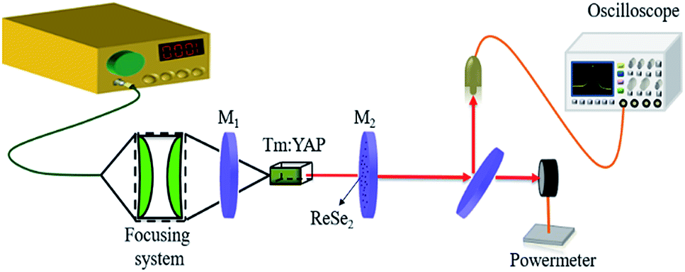 | ||
| Fig. 4 Experimental configuration of PQS Tm:YAP laser. | ||
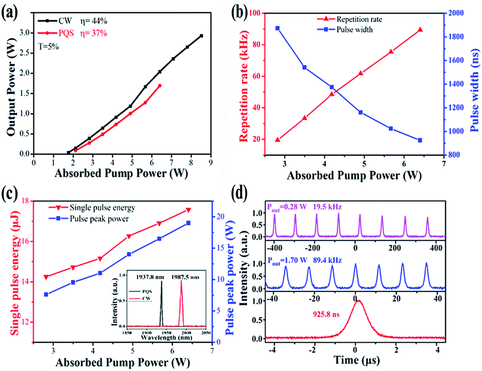
First, CW laser operation regime was achieved by using an output mirror (OM, T = 5%) without the ReSe2-SA. To protect the gain medium, the maximum absorbed pump power was limited to 8.5 W. A maximum CW output power of 2.9 W was obtained with a slope efficiency of 44%. Then, by substituting ReSe2 SAM for the plane OM and carefully aligning its position, the PQS operation of the Tm:YAP laser at 2 μm was realized. At the absorbed pump power of 6.4 W, the highest PQS average output power of 1.7 W was achieved, corresponding to a slope efficiency of 37%. While increasing pump power, the ReSe2 sample got damaged. Fig. 5(a) shows the output power of the CW and PQS laser operations versus the absorbed pump power, respectively. Compared to the CW laser operation, the PQS laser threshold was slightly raised from 1.68 W to 2.55 W and the slope efficiency was dropped from 44% to 37% on account of insertion loss.
 | ||
| Fig. 5 Laser properties versus absorbed pump power: (a) CW and PQS output power (b) pulse repetition rate and pulse duration, (c) single pulse energy and peak power; inset: laser spectra, and (d) pulse train and single pulse profile. | ||
The Q-switched pulse trains and profiles were detected by a fast InGaAs photodetector (Newport, Model 818-BB-51) with a rise time of 35 ps and recorded with a digital oscilloscope (Tektronix DPO 7104C, 1 GHz bandwidth, 20 Gs s−1 sampling rates). Fig. 5(b) presents the pulse repetition rate and width as a function of absorbed pump power. In the stable PQS regime, the pulse repetition rate and width varied from 19.5 kHz to 89.4 kHz and 1.8 μs to 925.8 ns, respectively. Under the highest absorbed pump power, the maximum pulse energy was reached to 17.6 μJ, corresponding to the maximum peak power of 19 W. The relationships between the pulse energy and peak power on the absorbed pump power are described in Fig. 5(c). The measured spectrum was inset in Fig. 5(c), it obviously illustrates that the central wavelength of CW laser is 1987.5 nm while it is 1937.8 nm for the Q-switched laser. The blueshift phenomenon were might be due to the high intracavity loss introduced by the ReSe2-SA. The typical pulse width of 925.8 ns and pulse repetition rate of 89.4 kHz are shown in Fig. 5(d). Fig. 6 shows the radio frequency (RF) spectrum of the output laser, and the signal-to-noise ratio (SNR) of the first beat was 30 dB at 89.4 kHz, indicating that the Q-switched laser pulse was relatively stable.
 | ||
| Fig. 6 The radio frequency spectra of the Q-switched pulses. | ||
Table 1 summarizes the 2 μm PQS Tm:YAP laser results ever achieved by employing nanomaterials as SAs. The BP Q-switched 2 μm laser in ref. 33 had higher peak power, pulse energy and shorter pulse width. However, the shortcoming of instability in air limited the application of BP in generating long-time stable pulsed laser. Compared with the other Nano-SAs, such as graphene, MoTe2, MoS2 and ReS2, our results could be considered superior than that. We believe that a better laser performance would be achieved by further optimizing the parameters of laser cavity and the characteristics of ReSe2-SA.
| Materials | SA | Pout (mW) | Slope efficiency | Pulse width (ns) | PRR (kHz) | Peak power (W) | Pulse energy (μJ) |
|---|---|---|---|---|---|---|---|
| Tm:YAP9 | Graphene | 362 | 6.8% | 735 | 42.4 | 11.6 | 8.5 |
| Tm,Ho:YAP17 | MoS2 | 270 | 5% | 435 | 55 | 11.3 | 4.9 |
| Tm:YAP19 | MoTe2 | 1210 | 34% | 380 | 144 | 22.2 | 8.4 |
| Tm:YAP33 | BP | 3100 | 48% | 181 | 81 | 218 | 39.5 |
| Tm:YAP34 | ReS2 | 245 | 19% | 415 | 67.7 | 8.72 | 0.36 |
| Tm:YAP (this work) | ReSe2 | 1700 | 37% | 925 | 89.4 | 19.0 | 17.6 |
5. Conclusions
In summary, the band structure of the ReSe2 with different ratios of Re and Se was calculated by VASP and the results were that Se atomic defects have the tendency to reduce the bandgap. The few-layered ReSe2-SA was prepared by LPE method and the saturable absorption effect was characterized around 2 μm. Using the as-prepared ReSe2-SA, a PQS 2 μm Tm:YAP laser was demonstrated for the first time, to the best of our knowledge. A maximum PQS average output power of 1.7 W was obtained, corresponding to an optical-to-optical and a slope conversion efficiency of 26.6% and 37%, respectively. The shortest pulse duration of 925.8 ns was realized with a pulse repetition rate of 89.4 kHz, resulting in the maximum single pulse energy and peak power of 17.6 μJ and 19.0 W, respectively. The results indicate that the feasibility of layered ReSe2 as SA for achieving high-efficient 2 μm pulsed lasers.Conflicts of interest
There are no conflicts to declare.Acknowledgements
This work was supported by the Key Research and Development Program of Shandong Province (2018GGX102005), the National Key Research and Development Program of China (2017YFA0701000), the Natural Science Foundation of Qingdao (18-2-2-11-jch),the NSFC programs (61775123) and the SDUST Research Fund (2019TDJH103).Notes and references
- T. Yokozawa and H. Hara, Appl. Opt., 1996, 35, 1424–1426 CrossRef CAS PubMed.
- P. Werle and F. Slemr, et al., Opt. Lasers Eng., 2002, 37, 101–114 CrossRef.
- V. Wulfmeyer, M. Randall and A. Brewer, et al., Opt. Lett., 2000, 25, 1228–1230 CrossRef CAS PubMed.
- H. L. Wang, W. Cai and F. Wang, et al., Opt. Quantum Electron., 2016, 48, 11 CrossRef.
- U. Keller, Nature, 2003, 424, 831–838 CrossRef CAS PubMed.
- M. Segura, M. Kadankov and X. Mateos, et al., Opt. Express, 2012, 20, 3394–3400 CrossRef CAS PubMed.
- T. Y. Tsai and M. Birnbaum, Appl. Opt., 2001, 40, 6633–6637 CrossRef CAS PubMed.
- J. Liu, Y. G. Wang and Z. S. Qu, et al., Opt. Laser Eng., 2012, 44, 960–962 CrossRef CAS.
- J. Hou, B. T. Zhang and J. L. He, et al., Appl. Opt., 2014, 53, 4968–4971 CrossRef CAS PubMed.
- Z. Luo, C. Liu and Y. Huang, et al., IEEE J. Sel. Top. Quantum Electron., 2014, 20, 0902708 Search PubMed.
- Y. Sun, C. Lee and J. Xu, et al., Photonics Res., 2014, 3, 97–101 CrossRef.
- J. Sotor, G. Sobon and M. Kowalczyk, et al., Opt. Lett., 2015, 40, 3885–3888 CrossRef CAS PubMed.
- D. Sebbag, A. Korenfeld and U. Ben-Ami, et al., Opt. Lett., 2015, 40, 1250–1253 CrossRef CAS PubMed.
- R. I. Woodward, R. C. T. Howe and T. H. Runcorn, et al., Opt. Express, 2015, 15, 20051–20061 CrossRef PubMed.
- M. Lin, Q. Peng and W. Hou, et al., Opt. Laser Eng., 2019, 109, 90–93 CrossRef CAS.
- C. Cong, J. Shang and Y. Wang, et al., Adv. Opt. Mater., 2017, 6, 1700767 CrossRef.
- C. Luan, X. Zhang and K. Yang, et al., IEEE J. Sel. Top. Quantum Electron., 2017, 23, 1600105 Search PubMed.
- X. Su, H. Nie and Y. Wang, et al., Opt. Lett., 2017, 42, 3502–3505 CrossRef CAS PubMed.
- B. Yan, B. Zhang and H. Nie, et al., Opt. Express, 2018, 26, 18505–18512 CrossRef CAS PubMed.
- L. Hart, S. Dale and S. Hoye, et al., Nano Lett., 2016, 16, 1381–1386 CrossRef CAS PubMed.
- F. Cui, X. Li and Q. Feng, et al., Nano Res., 2017, 10, 2732–2742 CrossRef CAS.
- D. Wolverson, S. Crampin and A. S. Kazemi, et al., ACS Nano, 2014, 8, 11154–11164 CrossRef CAS PubMed.
- H. Wang, E. Liu and Y. Wang, et al., Phys. Rev. B, 2017, 96, 165418 CrossRef.
- H. Zhao, J. Wu and H. Zhong, et al., Nano Res., 2015, 8, 3651–3661 CrossRef CAS.
- H. Zhong, S. Gao and J. Shi, et al., Phys. Rev. B: Condens. Matter Mater. Phys., 2015, 92, 115438 CrossRef.
- C. Fang, G. Wiegers and C. Haas, et al., J. Phys.: Condens. Matter, 1997, 9, 4411–4424 CrossRef CAS.
- L. Du, G. Jiang and L. Miao, et al., Opt. Mater. Express, 2018, 8, 926–935 CrossRef CAS.
- Z. Li, N. Dong and Y. Zhang, et al., APL Photonics, 2018, 3, 080802 CrossRef.
- L. Chun, Y. Leng and J. Huo, Chin. Opt. Lett., 2019, 17, 011402 CrossRef.
- G. Kresse and J. Hafner, Phys. Rev. B: Condens. Matter Mater. Phys., 1993, 47, 558–561 CrossRef CAS.
- J. Perdew and K. Burke, et al., Phys. Rev. Lett., 1996, 77, 3865–3868 CrossRef CAS PubMed.
- P. Yasaei, B. Kumar and T. Foroozan, et al., Adv. Mater., 2015, 27, 1887–1892 CrossRef CAS PubMed.
- H. K. Zhang, J. L. He and Z. W. Wang, et al., Opt. Mater. Express, 2016, 6, 2328–2335 CrossRef CAS.
- X. C. Su, B. T. Zhang and Y. R. Wang, et al., Photonics Res., 2018, 6, 498–505 CrossRef CAS.
Footnote |
| † Yongping Yao and Xiaowen Li contributed equally to this work. |
| This journal is © The Royal Society of Chemistry 2019 |