
 Open Access Article
 This Open Access Article is licensed under a Creative Commons Attribution-Non Commercial 3.0 Unported Licence
Multiple-engineering controlled growth of tunable-bandgap perovskite nanowires for high performance photodetectors†
Kuankuan Ren ab,
Jian Wangc,
Kong Liuab,
Yanbin Huangab,
Yang Sunab,
Muhammad Azamab,
Peng Jinc,
Zhijie Wang*ab,
Shengchun Qu*ab and
Zhanguo Wangab
ab,
Jian Wangc,
Kong Liuab,
Yanbin Huangab,
Yang Sunab,
Muhammad Azamab,
Peng Jinc,
Zhijie Wang*ab,
Shengchun Qu*ab and
Zhanguo Wangab
aKey Laboratory of Semiconductor Materials Science, Beijing Key Laboratory of Low Dimensional Semiconductor Materials and Devices, Institute of Semiconductors, Chinese Academy of Sciences, Beijing, 100083, China. E-mail: wangzj@semi.ac.cn; qsc@semi.ac.cn
bCenter of Materials Science and Optoelectronics Engineering, University of Chinese Academy of Sciences, Beijing 100049, China
cResearch Center of Ultra-Precision Optoelectronic Instrument, Harbin Institute of Technology, Harbin 150080, China
First published on 25th June 2019
Abstract
Controllable growth of perovskite nanowires is very important for various applications in optical and electrical devices. Although significant progress has been achieved in the solution method, a deep understanding of the mechanics of growing perovskite nanowires is still lacking. Herein, we developed an electrochemical method for growing the perovskite nanowires and studied the growth processes systematically. The initial nucleation and crystal growth could be controlled by simply varying the additive solvents, thus leading to two stable size ratio distributions of the perovskite nanowires. Further, with compositional engineering, the bandgap of the perovskites could be tuned from 1.59 eV to 3.04 eV. All the as-grown perovskite nanowires displayed a unique structure with high crystallization quality, contributing to a very high responsivity of 2.1 A W−1 and a large on/off ratio of 5 × 10³ for the photodetectors based on the CH3NH3PbBr3 nanowires. All of these findings demonstrate that the optimized solution method offers a new approach to synthesize perovskite nanowires for applications in photoelectric devices.
Hybrid organic–inorganic perovskite materials have changed the existing landscape in photovoltaic research owing to their exceptional optoelectronic performance parameters, such as long carrier lifetimes, long carrier diffusion lengths, high absorption coefficient and high carrier mobility.1–5 These fascinating properties boosted the latest certified power conversion efficiency of the perovskite solar cells up to 23.7%, inspiring researchers greatly to develop applications for perovskite devices.6,7 Therefore, abundant studies explored the applications of perovskite light emitting diodes (LED), lasers and photodetectors.8–13 Most of these devices are primarily based on polycrystalline perovskite thin films, single crystals or nanomaterials. Particularly, the perovskite nanomaterials have become a new research field for optoelectronic applications due to their unique morphologies and extraordinary performances. The corresponding perovskite nanodevices display outstanding quantum yields, high photosensitivity, photoelectric conversion efficiency and long-term stability,14–17 surpassing those of original material systems. Therein, perovskites nanowires, as the building blocks of optoelectronic integrated devices, have aroused extensive research interests due to their well-defined structures.18–21
The properties of the nanowires are highly dependent on growth techniques. Up to now, various fabrication technologies have been developed for growing perovskite nanowires, including chemical vapor deposition22–24 and template-assisted synthesis methods,25–27 which are based on high temperature processes or extra template assistance. However, perovskite nanowires can be converted directly from the perovskite thin films or supersaturated perovskite precursor solutions by evaporating the additional solvent without any template in easy-controlled solution methods.28–31 Although their corresponding devices show promising performances, the nanowires seem to show rough surfaces or large boundaries that limit further performance improvement. There is also an optional solution method, where the perovskite nanowires can be grown by reacting lead acetate (PbAc2) or lead halide (PbX2, X = I, Br, Cl) thin films with methylammonium halides (CH3NH3Y, Y = I, Br, Cl) in isopropanol solution.8,32,33 These nanowires exhibited smooth surfaces and high crystallinity. Nevertheless, most of these studies focus only on one kind of halide perovskite growth. Even other halide perovskites can be transformed by ion-exchange reactions, which also suffer from poor morphology retention.32 It is increasingly necessary to develop a suitable method for the growth of all kinds of halide perovskites. Besides, there is also a lack of systematic research on the dimension controlled growth of full halide perovskite nanowires. For producing the full kind of halide perovskites, the initial lead salt film also needs to be changed.
Herein, we have developed a solution method based on the electrochemical growth of lead oxide (PbO2) to replace the drop-cast lead salt film as the reaction precursor. By adding additive solvents, compositional or temperature engineering for controlling the growing processes, pure halide CH3NH3PbX3 (X = Br, Cl, I) and mixed halide perovskite nanowires were synthesized with adjusted diameter distribution. The as-grown perovskite nanowires showed good growing repeatability and high crystallinity. Finally, the photodetectors based on these perovskite nanowires exhibited high responsivity and a large on/off ratio.
In the first step, we deposited a PbO2 film on the ITO substrate in the prepared aqueous solution. After that, the perovskite nanowires were synthesized by immersing the electrochemically deposited PbO2 film in different CH3NH3X isopropanol solutions. By controlling the concentration, additive solvents or the growth temperature in the reaction environment, perovskite nanostructures with different size distributions could be grown. All the shapes of the grown perovskite samples and their detailed growth conditions are shown in Table 1. During the growth of the CH3NH3PbBr3 nanowires, Fig. 1 shows that the highest concentration of CH3NH3Br led to shorter and thicker nanowires, which are surrounded by many large nanocrystals. However, longer and thinner nanowires were obtained with lower concentrations of CH3NH3Br. More importantly, a smooth perovskite crystalline layer was formed in areas without any nanostructure coverage. The crystalline layer might act as a barrier for the reaction of CH3NH3Br with PbO2, thus reducing the nucleation rate and sites for the perovskite wires, and could further promote the anisotropic growth of nanowires. These effects are also in agreement with previous reports,8 which reveal that the initial perovskite layer can inhibit the continual diffusion of CH3NH3+ ions to react with the lead salts. The powder XRD (X-ray diffraction) spectra in Fig. S1† showed the position of the characteristic diffraction peaks at 14.9°, 21.2°, 30.2° and 33.8°, which can be indexed to the (001), (011), (002) and (021) crystal planes, respectively. There was no peak at 36.4° during the growth of perovskites except for the initially deposited PbO2 thin film, indicating full conversion into CH3NH3PbBr3 at different concentrations of CH3NH3Br. To illustrate the growth mechanism of the synthesized perovskite nanowires, the effect of growth time on morphology was investigated. Fig. S2† displays the final SEM images of the perovskite nanowires grown at different reaction times at the concentration of 10 mg mL−1 CH3NH3Br/isopropanol. These initial nuclei grow to form perovskite nanowires, nanorods or nanocubes during the first 20 minutes. Thus, initial nucleation may be the key shape-determinant step for CH3NH3PbBr3 morphology. With the reaction time further increasing from 1 h to 4 h, the diameters increased slowly due to the dissolution–recrystallization processes. Consequently, the nanowires dominated the CH3NH3PbBr3 sample with high crystalline order. Considering the above experimental results and previous studies,34–36 the potential growth processes can be written as follows:
| CH3NH3Br ↔ CH3NH2 + HBr | (1) |
| PbO2 + 4HBr → PbBr2 + 2H2O + Br2 | (2) |
| PbBr2 + CH3NH3Br → CH3NH3PbBr3 | (3) |
| PbO2 + 5CH3NH3Br → CH3NH3PbBr3 + 4CH3NH2 + 2H2O + Br2 | (4) |
| No. | Solute | Solvents | Perovskite | Nanostructures | SEM |
|---|---|---|---|---|---|
| 1 | MABr (20, 10, 5, 2 mg mL−1) | ISP | MAPbBr3 | NW, NC, NP | Fig. 1 and S1 |
| 2 | MABr (10 mg mL−1) | ISP + H2O | MAPbBr3 | NW | Fig. S3 |
| 3 | MABr (10 mg mL−1) | ISP + DMF | MAPbBr3 | NW, NC | Fig. 2 |
| 4 | MABr (10 mg mL−1) | ISP + DMF | MAPbBr3 | NC | Fig. 3 |
| 5 | MABr (10 mg mL−1) | ISP + DMSO | MAPbBr3 | NP, NW | Fig. S7 |
| 6 | MAI (20, 10, 5 mg mL−1) | ISP | MAPbI3 | NC | Fig. S9 |
| 7 | MAI (10 mg mL−1) | ISP + DMF | MAPbI3 | NW | Fig. 4a, b and S12 |
| 8 | MAI (10 mg mL−1) | ISP + DMSO | MAPbI3 | NW | Fig. 4c, d and S11 |
| 9 | MACl (6 mg mL−1) | ISP + DMF | MAPbCl3 | NW | Fig. 5b |
| 10 | MACl (6 mg mL−1) | ISP + DMSO | MAPbCl3 | NW | Fig. 5c |
| 11 | MACl (6 mg mL−1) | ISP (heating) | MAPbCl3 | NW | Fig. 5d |
| 12 | MACl1−xIx (18 mg mL−1) | ISP | MAPbCl3−xBrx | NP | Fig. S13 |
| 13 | MACl1−yBry (7.2, 8, 8.8 mg mL−1) | ISP | MAPbCl3−yBry | NW | Fig. S14 |
| 14 | MABr1−zIz (10 mg mL−1) | ISP | MAPbBr3−zIz | NC, NW | Fig. S15 |
 | ||
| Fig. 1 The SEM images of perovskite CH3NH3PbBr3 nanostructures grown at different concentrations of CH3NH3Br in the isopropanol solution. (a) 20 mg mL−1, (b) 10 mg mL−1, (c) 5 mg mL−1, (d) 2 mg mL−1. | ||
Briefly, CH3NH3Br firstly decomposes to methylamine (CH3NH2) and hydrogen bromide (HBr) in the isopropanol solvent with a reversible equilibrium (eqn (1)). The released HBr reacts quickly with PbO2 to form lead bromide (PbBr2) on dipping the PbO2 film into the above-mentioned CH3NH3Br solution (eqn (2)). Thus, it facilitates the shift of eqn (1) towards the positive direction to keep the reaction balance, leading to a positive decomposition of CH3NH3Br for providing HBr to reduce Pb4+ to Pb2+. As the reaction goes on, PbBr2, in turn, reacts quickly with the excess CH3NH3Br solute and eventually grows into CH3NH3PbBr3 due to the low activation energy required in this conversion process (eqn (3)). Consistent with our experimental results, no typical diffraction peaks of PbBr2 could be detected in the PXRD patterns (Fig. S1†). The total reaction equations are summed up in eqn (4), which shows that water molecules (H2O) are the byproducts of the final perovskite formation. To elucidate the role of H2O in the perovskite growth process, additional water molecules were added in the CH3NH3Br isopropanol solution. Fig. S3† shows that the nanocubes occupied a large ratio of the nanostructures at a low concentration of H2O and the nanowires grew only at the intervals of the nanocubes. At a high concentration of H2O, all the nanostructure growth processes were inhibited, resulting in the formation of a CH3NH3PbBr3 film. The PXRD patterns in Fig. S4† show two new peaks of PbBr2 appearing at 17.7° and 35.9° when the H2O content reached up to 80 μL, indicating the decomposition of the perovskite CH3NH3PbBr3.37 However, an appropriate amount of H2O is also beneficial to the crystal growth of perovskite, as previous articles have reported.38 These results indicated that, if we could control the reaction processes in eqn (4), the growth of perovskite nanostructures could be manipulated. Fortunately, we found methods to change the reaction environment by adding an additional solvent to the precursor solution.
Fig. 2a–f show the SEM images of the CH3NH3PbBr3 nanowires grown with different added volumes of DMF in 1 mL isopropanol solution of CH3NH3Br (10 mg mL−1). The growth time was set at 4 h to ensure a complete reaction of PbO2 with CH3NH3Br. Fig. 2g shows that the average length of the nanowire increased from a few microns to 20 microns as the DMF concentration increased. Fig. 2h shows that all the diffraction peaks could be well indexed to the as-synthesized perovskite CH3NH3PbBr3, indicating good crystallization. The morphology of the CH3NH3PbBr3 nanowires varied greatly with the change in DMF concentration, which illustrates that DMF is a crucial factor for the final morphology of the perovskite nanostructures. As the DMF concentration increased, the nanowires exhibited a larger dimension, lower density and broader size distribution. The nanowires even presented two stable size ratio distributions (length ∼ 3 μm with width ∼ 100 nm and length ∼ 20 μm with width ∼ 800 nm) when the DMF volume increased to 50 μL. This phenomenon has been rarely reported so far. Synthesizing perovskite nanowires of sizes smaller than 100 nm via this method is more difficult than that via the colloidal synthetic methods.39,40 These results could be attributed to the dissolution–recrystallization processes facilitated by DMF, which controls the nucleation and seed growth stages, based on the kinetic theory.28 Due to the high solubility of perovskite in DMF, the initial nucleation of the perovskite was inhibited, thus moderating the perovskite crystal growth processes. However, when the perovskite in the mixed solutions reached supersaturation, DMF could not only provide the source materials for nanowire growth but also induce the formation of new nucleation sites. Thus, a broader size distribution of the nanowires was obtained. In addition, the formation of nanowires smaller than 100 nm in size was due to the new nucleation sites, which are discussed in detail below. The new nucleation sites could have hindered nanowire growth by consuming all the newly formed perovskites, thus leading to the formation of the perovskite film (Fig. S5†).
 | ||
| Fig. 2 The SEM images of the perovskite CH3NH3PbBr3 nanowires grown with different added volumes of DMF in 1 mL isopropanol. (a) 10 μL, (b) 20 μL, (c) 50 μL, (d) 80 μL, (e) 100 μL, (f) the magnified image of a selected area in (e). (g) The corresponding length distributions and (h) PXRD patterns. | ||
In order to confirm the above-mentioned hypothesis that DMF affects the final morphology of the CH3NH3PbBr3 nanowires, the nanowires grown at different reaction times were investigated. During the initial formation of CH3NH3PbBr3, the initial nucleation sites were scattered on the surface of the PbO2 film (Fig. 3a). The number of nucleation sites was significantly reduced compared with that without DMF (Fig. S2†), which confirms our assumption that the DMF can inhibit the initial nucleation of the perovskite nanostructures. When the growth time increased from 1 min to 30 min, the nanocubes tended to grow quickly with a lower density at the expense of sacrificing the small grains; some nanowires also started to grow from the nanocubes (Fig. 3a–c). As the reaction time further increased to 60 min, the nanowires grew longer and thicker with a high density (Fig. 3d). Very thin nanowires had also begun to form in some areas (Fig. S6†). These results are well consistent with our above explanation that DMF can induce new nucleation sites when the perovskite reaches supersaturation in mixed solutions, thus leading to the formation of thinner nanowires after reacting for several tens of minutes. The corresponding diameter distributions were counted, as shown in Fig. 3e and f. All the diameter distributions presented good Gaussian curves, where the mean diameter increased from 450 nm to 900 nm along with the increase in the reaction time. Besides, to illustrate that the role of DMF is not unique, we also investigated the effect of DMSO on the growth of the perovskite CH3NH3PbBr3. As the DMSO concentration increased, the morphology of CH3NH3PbBr3 transformed from nanowires to nanoplates (Fig. S7†), and the PXRD patterns also confirmed the change as the diffraction peak at 21.2° disappeared apparently (Fig. S8†). The direction of thickness growth was consistent with the dominant (001) series of crystal planes in the XRD patterns.41 The CH3NH3PbBr3 film was also formed when the content of DMSO increased to 200 μL, although a new peak belonging to PbBr2 emerged at 35.2°. On further controlling the crystallization process of the perovskite by adjusting the amount of the extra additive DMSO, high-quality single crystal perovskite CH3NH3PbBr3 films could be obtained.
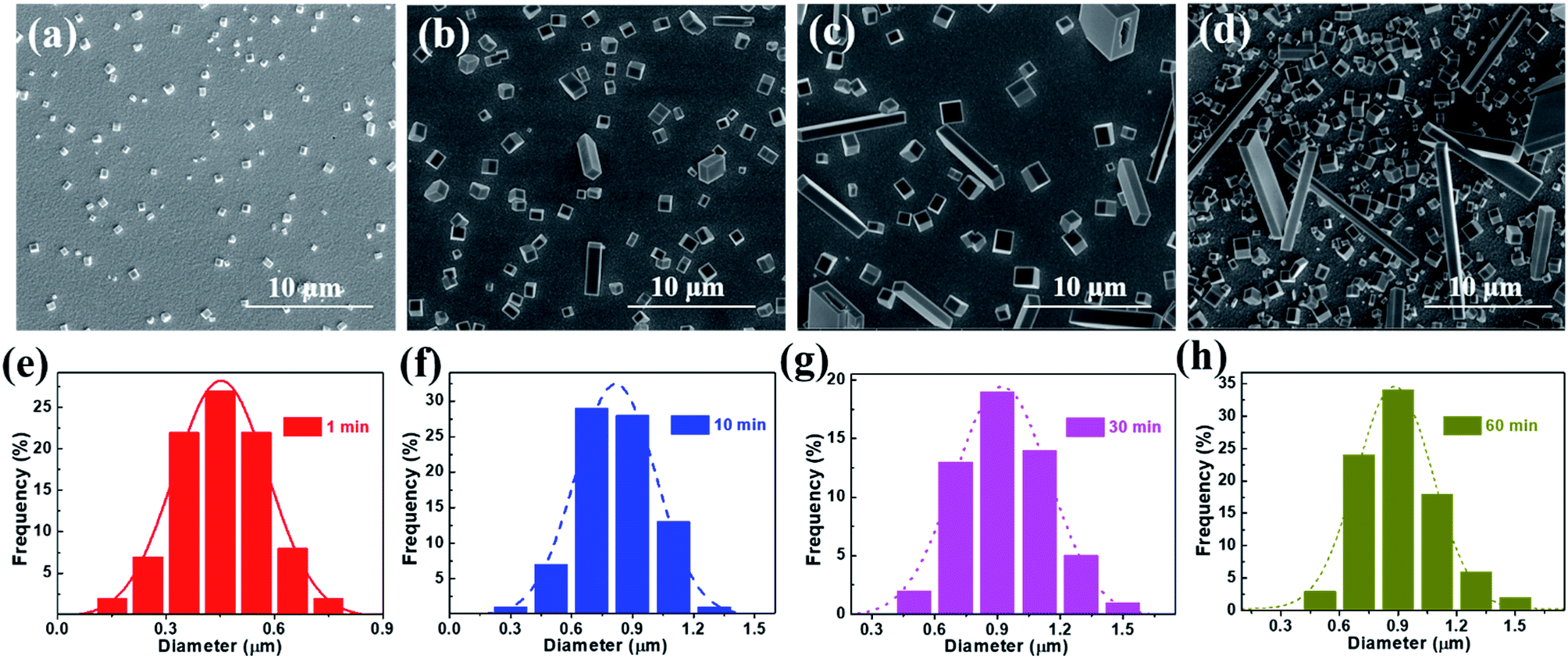 | ||
| Fig. 3 The nanostructures of perovskite CH3NH3PbBr3 grown at various reaction times: (a) 1 min, (b) 10 min, (c) 30 min and (d) 60 min. The precursor CH3NH3Br/ISP solution was at a stable concentration of 10 mg mL−1 with 100 μL DMF additive. The corresponding diameter distributions during the initial nucleation and crystal growth of the perovskite are shown in (e)–(h), respectively. The various colored (dashed) lines are the Gaussian fitting curves of the statistical histograms. | ||
To illustrate the universality of our approach, we extended it to synthesize various compositional perovskite nanowires just by replacing CH3NH3Br with other halide precursors as the starting solute. Although in the initial step, the perovskite CH3NH3PbI3 could be only grown into cube-like nanostructures at different concentrations of CH3NH3I (Fig. S9†), ultralong (hundred microns) white-phase CH3NH3PbI3 nanowires could be formed when DMF was added in the MAI/ISP solution (Fig. 4a). This is consistent with previous studies,42,43 which report that CH3NH3I–PbI2–DMF intermediate phases can be formed in the mixed solution despite different initial lead salt films. After annealing at 100 °C for 15 min, the color of the perovskite gradually changed from white to black. Fig. 4b shows the morphology of the grown perovskite without any changes after annealing, illustrating that pure perovskite CH3NH3PbI3 nanowires can be formed from CH3NH3I–PbI2–DMF intermediate phases. Besides, Fig. 4c and d show that DMSO has the same effect as DMF; that is, the nanowires could be transformed from the intermediate phase of CH3NH3I–PbI2–DMSO after annealing. The PXRD patterns in Fig. S10† confirmed the intermediate phases of CH3NH3I–PbI2–DMF and CH3NH3I–PbI2–DMSO formed after the corresponding solvents were added.
 | ||
| Fig. 4 The SEM images of perovskite CH3NH3PbI3 nanowires (a) grown with 30 μL DMF added into 1 mL isopropanol solution and (b) the corresponding samples after annealing at 100 °C for 15 minutes. The perovskite CH3NH3PbI3 nanowires (c) grown with 10 μL DMSO added into the isopropanol solution and (d) the corresponding samples after annealing at 100 °C for 15 minutes. The concentration of MAI/ISP solution was 10 mg mL−1. | ||
The presence of CH3NH3PbI3 characteristic peaks (red lines) illustrated the synthesis of perovskite CH3NH3PbI3 after annealing. Although a little peak of PbI2 emerged at 12.7°,8 the pure perovskite CH3NH3PbI3 nanowires could be formed by optimizing the growth parameters. Fig. S11 and S12† show that the intermediate phases of CH3NH3PbI3 could be synthesized at different concentrations of DMF and DMSO, respectively. Considering that the annealing processes did not affect the final morphology of the perovskite products, we believed that the corresponding pure perovskite CH3NH3PbI3 nanowires could be obtained after annealing.
For CH3NH3PbCl3, no change in the PbO2 film could be observed when we immersed the PbO2 film in CH3NH3Cl isopropanol solution for more than ten hours (Fig. 5a). This result illustrated that they could not react with each other due to the high nucleation energy required at room temperature. However, when an extra additive of 50 μL DMF or DMSO was added in the CH3NH3Cl isopropanol solution, the perovskite CH3NH3PbCl3 nanowires could be grown within hours. The extra additive solvents could act as a catalyst, which provides an intermediary process for the growth of CH3NH3PbCl3. As shown in Fig. 5b and c, the CH3NH3PbCl3 nanowires grew on the substrate with a large pitch distribution. Fig. 5d shows that the CH3NH3PbCl3 nanowires could also grow at a high reaction temperature within dozens of minutes, indicating that the nucleation barrier could be overcome effectively. The broader size distributions of the nanowires can be attributed to the simultaneous occurrence of nucleation and crystal growth processes.
 | ||
| Fig. 5 The SEM images of the perovskite CH3NH3PbCl3 nanostructures grown at different reactive environments. (a) Room temperature without DMF in isopropanol solution, (b) 50 μL DMF in 1 mL isopropanol solution, (c) 50 μL DMSO in 1 mL isopropanol solution, and (d) 80 °C. The concentration of MACl/ISP solution was 6 mg mL−1. | ||
According to our previous research,44 mixed halides play an important role in the growth of perovskite nanostructures. We have shown that the CH3NH3PbCl3−xIx nanoplates can be grown at a specific concentration ratio. When we immersed the PbO2 film in the solution with 1![[thin space (1/6-em)]](https://www.rsc.org/images/entities/char_2009.gif) :1 concentration ratio of CH3NH3Cl and CH3NH3I, nanoplates could be generated (Fig. S13†). The mixed halide perovskite CH3NH3PbCl3−yBry and CH3NH3PbBr3−zIz nanowires could be grown at different halide ratios of CH3NH3I:CH3NH3Br and CH3NH3Br:CH3NH3Cl in isopropanol solution, respectively (Fig. S14 and S15†). The PXRD patterns in Fig. 6a display that the major characteristic diffraction peaks of the multiple component perovskites can shift from 15.6° to 14° as the halide changes from chloride to iodide gradually, illustrating that the mixed halide perovskites grew with expected crystal structures. These results are in agreement with similar reports.45–47 On increasing the x value of CH3NH3I1−xBrx and CH3NH3Br1−xClx in the reactive isopropanol solution, the x in the synthesized perovskite CH3NH3PbI3−xBrx and CH3NH3PbBr3−xClx will be increased too. Thus, perovskites with different compositions can be obtained. This wide component control of perovskites led to broad wavelength tunability. As shown in Fig. 6b, the fluorescence emission spectra of the as-grown perovskites could change from near-infrared (779 nm) to blue (408 nm), covering the full visible region. The corresponding optical bandgap (Eg) could be calculated approximately, according to the equation Eg = 1240/λ,48 where λ is the central wavelength of the emission spectrum. From the derived peak positions of λ, the Eg values were estimated in the range of 3.04–1.59 eV, which correlated well with previous studies.49
:1 concentration ratio of CH3NH3Cl and CH3NH3I, nanoplates could be generated (Fig. S13†). The mixed halide perovskite CH3NH3PbCl3−yBry and CH3NH3PbBr3−zIz nanowires could be grown at different halide ratios of CH3NH3I:CH3NH3Br and CH3NH3Br:CH3NH3Cl in isopropanol solution, respectively (Fig. S14 and S15†). The PXRD patterns in Fig. 6a display that the major characteristic diffraction peaks of the multiple component perovskites can shift from 15.6° to 14° as the halide changes from chloride to iodide gradually, illustrating that the mixed halide perovskites grew with expected crystal structures. These results are in agreement with similar reports.45–47 On increasing the x value of CH3NH3I1−xBrx and CH3NH3Br1−xClx in the reactive isopropanol solution, the x in the synthesized perovskite CH3NH3PbI3−xBrx and CH3NH3PbBr3−xClx will be increased too. Thus, perovskites with different compositions can be obtained. This wide component control of perovskites led to broad wavelength tunability. As shown in Fig. 6b, the fluorescence emission spectra of the as-grown perovskites could change from near-infrared (779 nm) to blue (408 nm), covering the full visible region. The corresponding optical bandgap (Eg) could be calculated approximately, according to the equation Eg = 1240/λ,48 where λ is the central wavelength of the emission spectrum. From the derived peak positions of λ, the Eg values were estimated in the range of 3.04–1.59 eV, which correlated well with previous studies.49
 | ||
| Fig. 6 (a) The PXRD patterns of the multiple compositional perovskite nanostructures grown at different halide ratios in the precursor solution. (b) Widely tunable fluorescence emission wavelength from the as-grown mixed halide perovskites. | ||
To investigate the optoelectronic properties of the perovskite nanowires synthesized by our method, photodetectors based on the CH3NH3PbBr3 nanowires were fabricated on a gold interdigital electrode, which was deposited on the quartz substrate with 60 nm in thickness under a designed macro mask plate. Fig. 7a shows the optical microscopy image of a real perovskite nanowire photodetector, where the nanowire is well located in the gap between the two separate electrodes. Upon illuminating with a 450 nm laser, the photocurrent shows an almost linear and symmetrical variation versus the voltage at different lasing power densities (Fig. 7b), indicating good ohmic contact between the perovskite and the gold electrode. Ohmic contact implies that the junction barrier between the gold electrode and perovskite is small, indicating that the hot electrons may also contribute to the high responsivity in photodetection.50 Under the applied voltage of 2 V, the photocurrent could reach 48 nA with light illumination at a power density of 83.3 mW cm−2. The dark current was as small as 0.01 nA, which could be extracted from the black line shown in Fig. 7b. Thus, the on/off ratio was calculated to be ∼5 × 10³, which is larger than those of the perovskite photodetectors reported recently.51,52 Fig. 7c plots the photocurrent and photoresponsivity against the light power under the same voltage of 2 V. The photocurrent shows a nearly linear upward trend with increasing light power, suggesting that the photoinduced carriers are proportional to the incident photons, which indicates fewer traps or defects in the obtained perovskite nanowires. The corresponding photoresponsivity R can be extracted from the equation R = Iph/PS, where Iph is the photocurrent, P is the incident light power, and S is the effective absorbing area of the photodetectors. Accordingly, the calculated R shows a decreasing trend from 2.1 to 0.6 A W−1 when the incident power increased from 2 to 25 mW. This may be because the carrier recombination was enhanced at high illumination power. As observed in the measurement process, the green fluorescence of the nanowire was very obvious under high irradiation. Even so, the photoresponsivity of the photodetectors could reach up to 2.1 A W−1, which is superior to those of the previously reported perovskite detectors.51–54 Besides the on/off ratio and responsivity characterization of the photodetector, the specific detectivity (D*) also acts as an important parameter that reflects the ability to detect weak light signals. Assuming that shot noise dominates the dark current, D* can be estimated from the expression D* = RS1/2/(2qId)1/2, where q is the unit charge and Id is the dark current.55 Thus, the maximum specific detectivity was then estimated to be 1.2 × 10¹² jones (jones = cm Hz1/2 W−1). For revealing the time response characteristics of the perovskite photodetectors, time-dependent photocurrent was measured, as shown in Fig. 7d. As soon as the photodetector was illuminated, the current rose drastically with a narrow peak due to the sudden excitation of carriers, which departed quickly and caused the photocurrent to stabilize.56 On blocking the light source, the current declined drastically. Similar current values cycled several times without much change under the light on and off conditions, displaying the good switching and repeatable performances of the photodetector. A high-resolution single cycle time response curve is shown in Fig. S16,† displaying a rise time of less than 0.9 s and a decay time of less than 0.2 s for the perovskite photodetector. Moreover, Fig. S17† also shows that the perovskite CH3NH3PbI3 nanowire photodetector is photoresponsive to the 450 nm laser, although the detection performance is inferior to that of the perovskite CH3NH3PbBr3 photodetector. This may be due to the rough surface and poor crystal quality of the perovskite CH3NH3PbI3 nanowires that were transformed from the intermediate phase.
 | ||
| Fig. 7 Optoelectronic property characterization of the perovskite CH3NH3PbBr3 nanowire photodetectors with 450 nm light irradiation. (a) Optical image of a perovskite nanowire photodetector. (b) Dark current and photocurrents of the perovskite nanowire photodetectors at various power densities. (c) Photocurrent and photoresponsivity measured at different illumination powers with a voltage of 2 V. (d) Time-dependent photocurrent curves of the perovskite nanowire photodetectors at a voltage of 10 V. | ||
Conclusions
In summary, we demonstrate that tunable bandgap perovskite nanowires can be synthesized by reacting the electrochemically deposited PbO2 film with the CH3NH3X (X = Br, I, Cl) or mixed halide solutes in isopropanol solution. By controlling the nucleation and growth processes with multiple engineering techniques, the structures and diameter distributions of the perovskite nanowires can be manipulated effectively. Although the nanowires grown by this method are cluttered on the substrate, we think this problem can be solved by the graphic deposition of lead oxide in the future. Looking forward, this simple electrochemically assisted controllable solution method could provide a new route for producing high-quality nanomaterials, especially perovskite nanomaterials, which are promising materials for applications in optoelectronic devices. For instance, the photodetectors we fabricated based on the CH3NH3PbBr3 nanowires exhibit a high responsivity of 2.1 A W−1 and an on/off ratio of 5 × 10³.Conflicts of interest
There are no conflicts to declare.Acknowledgements
This work was mostly supported by the Key Research Program of Frontier Science, Chinese Academy of Sciences (Grant No. QYZDB-SSW-SLH006), the National Key Research and Development Program of China (Grant No. 2017YFA0206600), the National Natural Science Foundation of China (Contract No. 61674141, 61504134 and 21503209). Z. W. also appreciates the support from Hundred Talents Program (Chinese Academy of Sciences).Notes and references
- Q. Dong, Y. Fang, Y. Shao, P. Mulligan, J. Qiu, L. Cao and J. Huang, Science, 2015, 347, 967–970 CrossRef CAS PubMed.
- T. M. Brenner, D. A. Egger, L. Kronik, G. Hodes and D. Cahen, Nat. Rev. Mater., 2016, 1, 15007 CrossRef CAS.
- Y. Liu, Z. Yang, D. Cui, X. Ren, J. Sun, X. Liu, J. Zhang, Q. Wei, H. Fan, F. Yu, X. Zhang, C. Zhao and S. F. Liu, Adv. Mater., 2015, 27, 5176–5183 CrossRef CAS PubMed.
- P. Yu, J. Wu, S. Liu, J. Xiong, C. Jagadish and Z. M. Wang, Nano Today, 2016, 11, 704–737 CrossRef CAS.
- U. Khan, Y. Zhinong, A. A. Khan, A. Zulfiqar and N. Ullah, Nanoscale Res. Lett., 2019, 14, 116 CrossRef PubMed.
- Anonymous, Nat. Energy, 2019, 4, 1 CrossRef.
- J. M. Buriak, P. V. Kamat, K. S. Schanze, A. P. Alivisatos, C. J. Murphy, G. C. Schatz, G. D. Scholes, P. J. Stang and P. S. Weiss, Chem. Mater., 2017, 29, 8915–8917 CrossRef CAS.
- H. Zhu, Y. Fu, F. Meng, X. Wu, Z. Gong, Q. Ding, M. V. Gustafsson, M. T. Trinh, S. Jin and X. Y. Zhu, Nat. Mater., 2015, 14, 636–642 CrossRef CAS PubMed.
- S. Bai, M. Cao, Y. Jin, X. Dai, X. Liang, Z. Ye, M. Li, J. Cheng, X. Xiao, Z. Wu, Z. Xia, B. Sun, E. Wang, Y. Mo, F. Gao and F. Zhang, Adv. Energy Mater., 2014, 4, 1301460 CrossRef.
- Y. Cao, N. Wang, H. Tian, J. Guo, Y. Wei, H. Chen, Y. Miao, W. Zou, K. Pan, Y. He, H. Cao, Y. Ke, M. Xu, Y. Wang, M. Yang, K. Du, Z. Fu, D. Kong, D. Dai, Y. Jin, G. Li, H. Li, Q. Peng, J. Wang and W. Huang, Nature, 2018, 562, 249–253 CrossRef PubMed.
- K. Lin, J. Xing, L. N. Quan, F. P. G. de Arquer, X. Gong, J. Lu, L. Xie, W. Zhao, D. Zhang, C. Yan, W. Li, X. Liu, Y. Lu, J. Kirman, E. H. Sargent, Q. Xiong and Z. Wei, Nature, 2018, 562, 245–248 CrossRef CAS PubMed.
- Y. Fang, Q. Dong, Y. Shao, Y. Yuan and J. Huang, Nat. Photonics, 2015, 9, 679–686 CrossRef CAS.
- S. Yakunin, D. N. Dirin, Y. Shynkarenko, V. Morad, I. Cherniukh, O. Nazarenko, D. Kreil, T. Nauser and M. V. Kovalenko, Nat. Photonics, 2016, 10, 585–589 CrossRef CAS.
- Y. Zhang, J. Liu, Z. Wang, Y. Xue, Q. Ou, L. Polavarapu, J. Zheng, X. Qi and Q. Bao, Chem. Commun., 2016, 52, 13637–13655 RSC.
- J. H. Im, J. Luo, M. Franckevicius, N. Pellet, P. Gao, T. Moehl, S. M. Zakeeruddin, M. K. Nazeeruddin, M. Gratzel and N. G. Park, Nano Lett., 2015, 15, 2120–2126 CrossRef CAS PubMed.
- K. Hong, Q. V. Le, S. Y. Kim and H. W. Jang, J. Mater. Chem. C, 2018, 6, 2189–2209 RSC.
- S. T. Ha, R. Su, J. Xing, Q. Zhang and Q. Xiong, Chem. Sci., 2017, 8, 2522–2536 RSC.
- X. Xu, X. Zhang, W. Deng, J. Jie and X. Zhang, Small Methods, 2018, 2, 1700340 CrossRef.
- W. Tian, C. Zhao, J. Leng, R. Cui and S. Jin, J. Am. Chem. Soc., 2015, 137, 12458–12461 CrossRef CAS PubMed.
- R. X. Yan, D. Gargas and P. D. Yang, Nat. Photonics, 2009, 3, 569–576 CrossRef CAS.
- F. P. García de Arquer and E. H. Sargent, Nat. Electron., 2018, 1, 380–381 CrossRef.
- S. T. Ha, X. Liu, Q. Zhang, D. Giovanni, T. C. Sum and Q. Xiong, Adv. Opt. Mater., 2014, 2, 838–844 CrossRef CAS.
- K. Park, J. W. Lee, J. D. Kim, N. S. Han, D. M. Jang, S. Jeong, J. Park and J. K. Song, J. Phys. Chem. Lett., 2016, 7, 3703–3710 CrossRef CAS PubMed.
- X. Wang, M. Shoaib, X. Wang, X. Zhang, M. He, Z. Luo, W. Zheng, H. Li, T. Yang, X. Zhu, L. Ma and A. Pan, ACS Nano, 2018, 12, 6170–6178 CrossRef CAS PubMed.
- Q. Zhou, J. G. Park, R. Nie, A. K. Thokchom, D. Ha, J. Pan, S. I. Seok and T. Kim, ACS Nano, 2018, 12, 8406–8414 CrossRef CAS.
- A. Waleed, M. M. Tavakoli, L. Gu, Z. Wang, D. Zhang, A. Manikandan, Q. Zhang, R. Zhang, Y. L. Chueh and Z. Fan, Nano Lett., 2017, 17, 523–530 CrossRef CAS.
- M. J. Ashley, M. N. O'Brien, K. R. Hedderick, J. A. Mason, M. B. Ross and C. A. Mirkin, J. Am. Chem. Soc., 2016, 138, 10096–10099 CrossRef CAS PubMed.
- P. Zhu, S. Gu, X. Shen, N. Xu, Y. Tan, S. Zhuang, Y. Deng, Z. Lu, Z. Wang and J. Zhu, Nano Lett., 2016, 16, 871–876 CrossRef CAS PubMed.
- E. Horvath, M. Spina, Z. Szekrenyes, K. Kamaras, R. Gaal, D. Gachet and L. Forro, Nano Lett., 2014, 14, 6761–6766 CrossRef CAS PubMed.
- L. Gao, K. Zeng, J. Guo, C. Ge, J. Du, Y. Zhao, C. Chen, H. Deng, Y. He, H. Song, G. Niu and J. Tang, Nano Lett., 2016, 16, 7446–7454 CrossRef CAS PubMed.
- W. Deng, X. Zhang, L. Huang, X. Xu, L. Wang, J. Wang, Q. Shang, S. T. Lee and J. Jie, Adv. Mater., 2016, 28, 2201–2208 CrossRef CAS PubMed.
- A. B. Wong, M. Lai, S. W. Eaton, Y. Yu, E. Lin, L. Dou, A. Fu and P. Yang, Nano Lett., 2015, 15, 5519–5524 CrossRef CAS PubMed.
- Y. Fu, F. Meng, M. B. Rowley, B. J. Thompson, M. J. Shearer, D. Ma, R. J. Hamers, J. C. Wright and S. Jin, J. Am. Chem. Soc., 2015, 137, 5810–5818 CrossRef CAS PubMed.
- J. A. Koza, J. C. Hill, A. C. Demster and J. A. Switzer, Chem. Mater., 2016, 28, 399–405 CrossRef CAS.
- H. Chen, Adv. Funct. Mater., 2017, 27, 1605654 CrossRef.
- J. H. Huang, K. J. Jiang, X. P. Cui, Q. Q. Zhang, M. Gao, M. J. Su, L. M. Yang and Y. Song, Sci. Rep., 2015, 5, 15889 CrossRef CAS PubMed.
- Y. X. Chen, Q. Q. Ge, Y. Shi, J. Liu, D. J. Xue, J. Y. Ma, J. Ding, H. J. Yan, J. S. Hu and L. J. Wan, J. Am. Chem. Soc., 2016, 138, 16196–16199 CrossRef CAS PubMed.
- J. You, Y. Yang, Z. Hong, T.-B. Song, L. Meng, Y. Liu, C. Jiang, H. Zhou, W.-H. Chang, G. Li and Y. Yang, Appl. Phys. Lett., 2014, 105, 183902 CrossRef.
- M. B. Teunis, A. Jana, P. Dutta, M. A. Johnson, M. Mandal, B. B. Muhoberac and R. Sardar, Chem. Mater., 2016, 28, 5043–5054 CrossRef CAS.
- C. Wang, Y. Zhang, A. Wang, Q. Wang, H. Tang, W. Shen, Z. Li and Z. Deng, Chem. Mater., 2017, 29, 2157–2166 CrossRef CAS.
- W. Zhang, L. Peng, J. Liu, A. Tang, J. S. Hu, J. Yao and Y. S. Zhao, Adv. Mater., 2016, 28, 4040–4046 CrossRef CAS PubMed.
- A. A. Petrov, N. Pellet, J.-Y. Seo, N. A. Belich, D. Y. Kovalev, A. V. Shevelkov, E. A. Goodilin, S. M. Zakeeruddin, A. B. Tarasov and M. Graetzel, Chem. Mater., 2016, 29, 587–594 CrossRef.
- A. A. Petrov, I. P. Sokolova, N. A. Belich, G. S. Peters, P. V. Dorovatovskii, Y. V. Zubavichus, V. N. Khrustalev, A. V. Petrov, M. Grätzel, E. A. Goodilin and A. B. Tarasov, J. Phys. Chem. C, 2017, 121, 20739–20743 CrossRef CAS.
- K. Ren, L. Huang, S. Yue, S. Lu, K. Liu, M. Azam, Z. Wang, Z. Wei, S. Qu and Z. Wang, J. Mater. Chem. C, 2017, 5, 2504–2508 RSC.
- N. K. Kumawat, A. Dey, A. Kumar, S. P. Gopinathan, K. L. Narasimhan and D. Kabra, ACS Appl. Mater. Interfaces, 2015, 7, 13119–13124 CrossRef CAS PubMed.
- A. Sadhanala, S. Ahmad, B. Zhao, N. Giesbrecht, P. M. Pearce, F. Deschler, R. L. Hoye, K. C. Godel, T. Bein, P. Docampo, S. E. Dutton, M. F. De Volder and R. H. Friend, Nano Lett., 2015, 15, 6095–6101 CrossRef CAS PubMed.
- A. Sadhanala, F. Deschler, T. H. Thomas, S. E. Dutton, K. C. Goedel, F. C. Hanusch, M. L. Lai, U. Steiner, T. Bein, P. Docampo, D. Cahen and R. H. Friend, J. Phys. Chem. Lett., 2014, 5, 2501–2505 CrossRef CAS PubMed.
- J. Dai, H. Zheng, C. Zhu, J. Lu and C. Xu, J. Mater. Chem. C, 2016, 4, 4408–4413 RSC.
- D. M. Jang, K. Park, D. H. Kim, J. Park, F. Shojaei, H. S. Kang, J. P. Ahn, J. W. Lee and J. K. Song, Nano Lett., 2015, 15, 5191–5199 CrossRef CAS PubMed.
- P. Yu, L. V. Besteiro, Y. Huang, J. Wu, L. Fu, H. H. Tan, C. Jagadish, G. P. Wiederrecht, A. O. Govorov and Z. Wang, Adv. Opt. Mater., 2018, 7, 1800995 CrossRef.
- S. Zhuo, J. Zhang, Y. Shi, Y. Huang and B. Zhang, Angew. Chem., Int. Ed. Engl., 2015, 54, 5693–5696 CrossRef CAS PubMed.
- J. Ding, S. Du, Z. Zuo, Y. Zhao, H. Cui and X. Zhan, J. Phys. Chem. C, 2017, 121, 4917–4923 CrossRef CAS.
- F. Chen, C. Xu, Q. Xu, Y. Zhu, F. Qin, W. Zhang, Z. Zhu, W. Liu and Z. Shi, ACS Appl. Mater. Interfaces, 2018, 10, 25763–25769 CrossRef CAS PubMed.
- F. Wang, J. Mei, Y. Wang, L. Zhang, H. Zhao and D. Zhao, ACS Appl. Mater. Interfaces, 2016, 8, 2840–2846 CrossRef CAS PubMed.
- D. Wang, J. Meng, X. Zhang, G. Guo, Z. Yin, H. Liu, L. Cheng, M. Gao, J. You and R. Wang, Chem. Mater., 2018, 30, 3819–3826 CrossRef CAS.
- D. Liu, Z. Hu, W. Hu, P. Wangyang, K. Yu, M. Wen, Z. Zu, J. Liu, M. Wang, W. Chen, M. Zhou, X. Tang and Z. Zang, Mater. Lett., 2017, 186, 243–246 CrossRef CAS.
Footnote |
| † Electronic supplementary information (ESI) available: Materials and methods, additional figures and discussions. See DOI: 10.1039/c9ra01689a |
| This journal is © The Royal Society of Chemistry 2019 |