
 Open Access Article
 This Open Access Article is licensed under a Creative Commons Attribution-Non Commercial 3.0 Unported Licence
Effect of interfacial defects on the electronic properties of graphene/g-GaN heterostructures
Zhongxun Deng ,
Xianhui Wang* and
Jie Cui
,
Xianhui Wang* and
Jie Cui
Shanxi Province Key Laboratory of Electrical Materials and Infiltration Technology, School of Materials Science and Engineering, Xi'an University of Technology, Xi'an 710048, Shaanxi, P. R. China. E-mail: xhwang693@xaut.edu.cn
First published on 1st May 2019
Abstract
To gain deep insights into their interactions, the effects of interfacial defects on the structural and electronic properties of graphene/g-GaN heterostructures were investigated by using first-principles calculations. The graphene/g-GaN-VGa heterostructure maintains a p-type Schottky contact in the spin-up channel and the Schottky barrier height (SBH) is decreased to 0.332 eV, but there is not a metal/semiconductor contact in the spin-down channel. However, the n-type SBH is negative for the graphene/g-GaN-VN heterostructure, indicating an ohmic contact. Furthermore, the SBH in the graphene/g-GaN heterostructure can be effectively modulated by the interlayer distance. The research could provide a strategy for the development and fabrication of efficient novel nanoelectronic devices.
1. Introduction
Recently, a great number of two-dimensional (2D) materials as promising candidates for next-generation electronic devices have been discovered and studied due to their outstanding properties.1–8 Graphene, a 2D sp2-hybridized carbon monolayer, is known to have many fascinating electronic and quantum transport properties, such as massless Dirac fermions, high carrier mobility and an intriguing quantum Hall effect, which makes it a potential material in nanoelectronic and related devices.9,10 Unfortunately, the gapless nature of graphene hinders its application in electronic devices.11,12 Despite considerable investigations toward bandgap opening in graphene, most of these methods are difficult to execute or they significantly sacrifice its high carrier mobility.Currently, vertical heterostructures based on 2D van der Waals (vdW) materials, which integrate the properties of their respective components with ideal properties, are considered a promising method to construct nanoelectronic and optoelectronic devices.13–18 Many 2D ultrathin hybrid graphene-based vdW heterostructures have been widely studied experimentally and theoretically, such as graphene/h-BN,19 graphene/BP,20 and graphene/TMDs.21 These graphene-based vdW heterostructures show novel optoelectronic properties far beyond their individual components. Moreover, for vdW heterostructures, most of the 2D materials form ideal substrates for each other to preserve their intrinsic electronic properties due to the lack of dangling bonds and the weak electron coupling between sublayers. For example, GaN thin films on a graphene layer exhibit excellent optical and electric characteristics and show promise for application in optoelectronic and electronic devices.22 Tian and his colleagues reported that a hybrid graphene/GaN phototransistor with a relatively large 15.2 mm2 active area can reach 361 mA W−1 at 10 V with a response time of only ∼5 ms, a much better performance than traditional GaN photodetectors.23 However, GaN in contact with flat graphene exhibits Schottky behavior.24 As we know, in a contact between metals and semiconductors the Schottky barrier is mainly contributed by the difference in Fermi level and associated charge transport. To date, in order to solve the problem of the contact barrier, many approaches have been developed to extend the possible applications of 2D heterostructures, for instance by changing interlayer distance, layer stacking or electric fields.25,26 There is a transition from an n-type to a Schottky type contact at the graphene/GaN interface when the interlayer distance decreases from 4.5 to 2.5 Å.27 Moreover, a band gap of up to 334 meV was obtained in graphene/graphene/GaN when the perpendicular electric field reached 1 V Å−1.28 Subsequently, understanding the interaction between g-GaN and graphene, and engineering the interfacial states are crucial for future applications.
In this work, the effect of structural defects on the interfacial states of graphene/GaN vdW heterostructures was investigated using first-principles calculations. Then, the effect of the interlayer coupling on the electronic properties of graphene/g-GaN heterostructures with defects was explored. For comparison, the effect of interlayer coupling on the electronic properties of graphene/g-GaN heterostructures without defects was also explored. The results exhibited that structural defects have a significant influence on the electronic properties of graphene/g-GaN vdW heterostructures. Moreover, tunable Schottky contacts and barrier can be achieved by modulating the interlayer coupling. The research is significant for the development and fabrication of efficient novel nanoelectronic devices.
2. Computational methods
This work used density functional theory (DFT) with the projected augmented wave (PAW) method, as implemented within the Vienna Ab-Initio Simulation Package (VASP).29–32 The generalized gradient approximation was utilized as the exchange–correlation functional, which can reasonably predict the band gap of GaN.33 The vdW correction proposed by Grimme was included in our calculations due to its good description of long-range vdW interactions.34 A dipole correction is considered in the z direction to remove the fake interaction between the dipole moments because the slab is not symmetric. The heterostructure calculations were performed using 5 × 5 × 1 and 13 × 13 × 1 Monkhorst–Pack K-point meshes for relaxation and electron static calculations, respectively. The Gaussian smearing method along the high symmetry line of Γ(0, 0, 0)–M(0, 1/2, 0)–K(−1/3, 2/3, 0)–Γ(0, 0, 0) and a broadening of 0.2 eV were adopted. The energy cutoff for plane-wave expansion was set to 450 eV. A large vacuum space of 20 Å was added to avoid interaction between adjacent images. All atoms were allowed to be fully relaxed until the atomic Hellmann–Feynman forces were smaller than 0.01 eV Å−1 and the convergence criterion of energy in the self-consistency process was set to 10−5 eV. Visualizations of supercells and structures were attained with the software VESTA.35The binding energy at the interface can be defined as
| Eb = [EGaN/graphene − (EGaN + Egraphene)]/NC, | (1) |
| Δρ = ρGaN/graphene − ρGaN − ρgraphene | (2) |
3. Results and discussion
3.1 Structural properties
Top views of the crystal structures of graphene/g-GaN without or with defects (Ga or N vacancies) are shown in Fig. 1. The calculated lattice constant of the free-standing graphene is 2.496 Å (ag = 2.496 Å), which is consistent with the experimental value.36 The optimized lattice constant of the GaN monolayer is 3.253 Å (aGaN = 3.253 Å), which agrees well with previous reports.37 It is generally known that graphene can be easily generated on a 6H-SiC substrate by epitaxial growth.38,39 Moreover,
  Å for graphene and 4aGaN = 13.012 Å for GaN. To minimize the lattice mismatch between the stacking sheets, a
  cell is adopted as the unit cell of graphene, whose lattice constant is 3.323 Å.40 For all the heterostructures considered in this work, supercells consisting of 3 × 3 unit cells of graphene and 4 × 4 unit cells of GaN without or with defects are adopted, which leads to a small lattice mismatch of 0.3% in the supercell. In the established models, the lattice constant of GaN is fixed and the lattice constant of graphene is changed to adjust the heterostructures. The supercells are then fully relaxed for the atomic geometry.
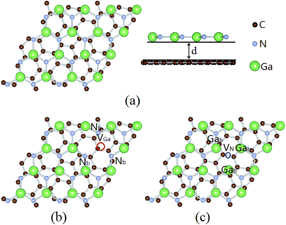 | ||
| Fig. 1 A schematic illustration of the crystal structures of graphene/g-GaN with or without defects: (a) graphene/g-GaN, (b) graphene/g-GaN-VGa, and (c) graphene/g-GaN-VN. | ||
The interlayer spacing (d), bond lengths (LC–C and LGa–N) and binding energy (Eb) for the considered structures are listed in Table 1. For g-GaN with VGa and VN, the interlayer spacing of the heterostructures are 3.287 and 3.225 Å, respectively, which are slightly smaller than that of the graphene/g-GaN heterostructure (3.296 Å). Moreover, their binding energies are 56 and 60 meV, which are the same order of magnitude as those of vdW crystals, such as MoS2/graphene,41 black phosphorene/graphene,42 or arsenene/graphene.43
| System | d (Å) | LC–C (Å) | LGa–N (Å) | Eb (meV C−1) |
|---|---|---|---|---|
| Graphene | 1.422 | |||
| GaN | 1.880 | |||
| Graphene/g-GaN | 3.296 | 1.422 | 1.880 | 54 |
| Graphene/g-GaN-VGa | 3.287 | 1.423 | 1.882 | 56 |
| Graphene/g-GaN-VN | 3.225 | 1.421 | 1.881 | 60 |
3.2 Electronic properties
The band structures of the graphene/g-GaN heterostructure without or with defects in its equilibrium configuration are shown in Fig. 2. From Fig. 2(a), it is evident that both the Dirac cone of graphene and the semiconducting nature of g-GaN are quite well preserved. The linear dispersion characteristic of graphene is retained in bands near the Fermi level. In addition, the Fermi level is located exactly at the Dirac cone, demonstrating that the effects of the interaction and charge transfer are vanishingly small. Compared with the band gap of 2.20 eV for free-standing GaN,44,45 the band gap of 1.893 eV for the g-GaN sublayer decreases when in contact with graphene. Furthermore, the bandgap width depends on the 2p orbit of N atoms in the g-GaN sublayer (Fig. 3(a)). These results suggest that graphene could be a very promising material for the metal electrode, and it could enhance the contact performance while the electronic properties of g-GaN could be sustained. Then, a Schottky barrier could be formed between graphene and g-GaN, which is similar to the coupling of graphene with BP or TMDs. Based on the Schottky–Mott rule, the corresponding Schottky barrier height (SBH) is determined by the energy levels of band edges in the semiconductor and Fermi levels in the metal. Here, the n-type SBH (ΦB,n) is defined as the energy difference between the conduction band minimum (CBM) of the g-GaN sublayer and the Dirac cone of the graphene sublayer, while the p-type SBH (ΦB,p) is defined as the energy difference between the Dirac cone of graphene and the valence band maximum (VBM) of the g-GaN sublayer. For the graphene/g-GaN heterostructure, the Dirac cone is close to the VBM of the g-GaN sublayer. The value of ΦB,p is 0.449 eV, much smaller than the value of 1.444 eV for ΦB,n. Hence, a p-type Schottky contact is formed at the graphene/g-GaN interface.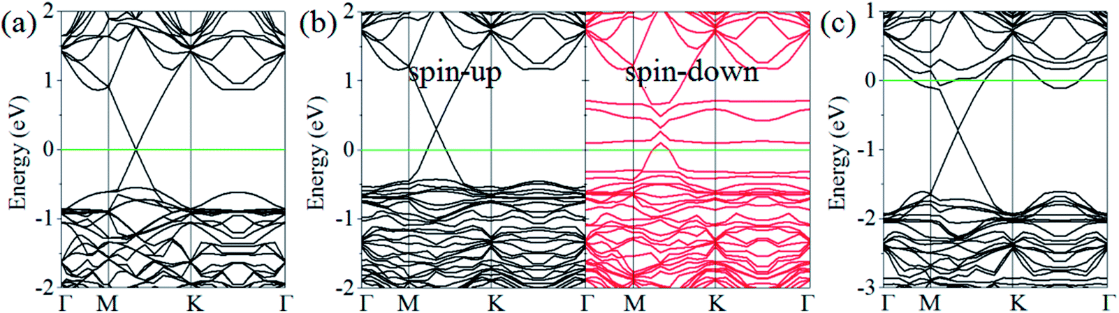 | ||
| Fig. 2 The band structure of graphene/g-GaN with or without defects: (a) graphene/g-GaN, (b) graphene/g-GaN-VGa, and (c) graphene/g-GaN-VN. | ||
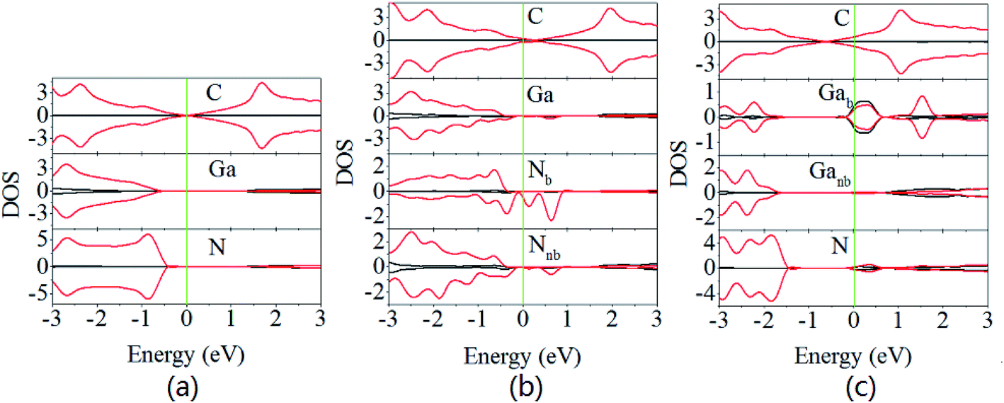 | ||
| Fig. 3 The partial density of states (DOS) of graphene/g-GaN with or without defects: (a) graphene/g-GaN, (b) graphene/g-GaN-VGa, and (c) graphene/g-GaN-VN. The black and red lines represent s and p orbitals of atoms, respectively. | ||
For the graphene/g-GaN-VGa heterostructure shown in Fig. 2(b), the semiconductor nature in the spin-up channel and the metallic character in the spin-down channel are quite well preserved for the GaN-VGa sublayer, while the Dirac cone is destroyed for the graphene sublayer. Moreover, the value of ΦB,p is 0.332 eV, much smaller than the value of 1.706 eV for ΦB,n in the spin-up channel. In addition, dangling bonds are produced on N atoms around the vacancy, inducing defect states between the VBM and CBM in the spin-down channel (Fig. 3(b)). However, g-GaN-VN exhibits an n-type semiconductor character in the graphene/g-GaN-VN heterostructure (Fig. 2(c) and 3(c)) and the value of ΦB,n is −0.158 eV, much smaller than the value of 1.454 eV for ΦB,p. Therefore, an ohmic contact is formed at the graphene/g-GaN-VN heterostructure.
Fig. 4 presents the electrostatic potential of graphene/g-GaN with or without defects. In the graphene/g-GaN heterostructure, the graphene layer has a deeper electrostatic potential than that of g-GaN. The difference between them across graphene/g-GaN is large, indicating a strong electronic field across the heterostructure. When there are Ga vacancies in g-GaN, the difference increases, while it decreases for g-GaN with N vacancies. Moreover, for the graphene/g-GaN and graphene/g-GaN-VGa heterostructures, the charges are depleted on the graphene side, while they are accumulated on the GaN side (Fig. 4(d) and (e)). The charges are depleted on the GaN-VN side, whereas they are accumulated on the graphene side for graphene/g-GaN-VN (Fig. 4(c)). The results of Bader charge population analysis show that the charge transfer from graphene to g-GaN (g-GaN-VGa) is 0.027e (0.059e), while the charge transfer from g-GaN-VN to graphene is 0.051e.
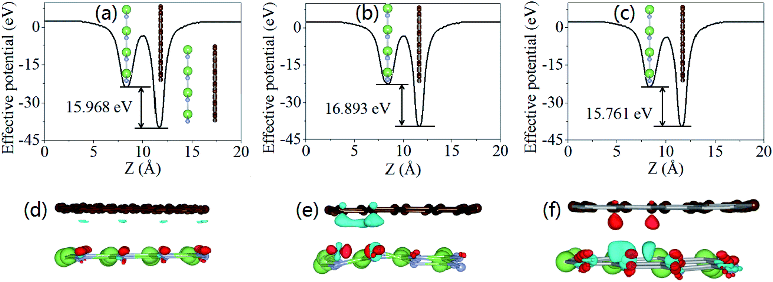 | ||
| Fig. 4 Electrostatic potentials and difference charge density of graphene/g-GaN (a), graphene/g-GaN-VGa (b), and graphene/g-GaN-VN (c). The corresponding differences in charge density are shown in (d)–(f). The red and cyan isosurfaces represent the gain and depletion of electrons, respectively. | ||
The above results show that the graphene/g-GaN, graphene/g-GaN-VGa, and graphene/g-GaN-VN heterostructures are p-type Schottky contact, p-type Schottky contact, and ohmic contact, respectively. Subsequently, for the design of graphene/GaN-based devices, structural defects might be desirable since they always improve the device performance. However, it is relatively well known that defect types are always uncontrolled during the fabrication of the g-GaN monolayer. Therefore, during fabrication of devices based on graphene/g-GaN heterostructures, it is essential to prepare g-GaN with defects, especially VN defects.
3.3 Effects of the interlayer coupling
It is important to explore the effect of interlayer coupling on the electronic properties of the heterostructures. The electronic states of graphene/g-GaN with or without defects with different interlayer distances (d) were calculated. For the graphene/g-GaN heterostructures, the results show that ΦB,p is always smaller than ΦB,n, which indicates that the p-type Schottky contact remains despite the variations in d. As the interlayer distance decreases from 3.143 Å to 2.969 Å, the values of ΦB,p are negative, suggesting that the p-type Schottky contact turns to an ohmic contact (Fig. 5(a)). For the graphene/g-GaN-VGa heterostructure, the electronic structures are almost unchanged and the p-type Schottky contact remains despite the variations in d (Fig. 5(b)). However, for the graphene/g-GaN-VN heterostructure, the values of ΦB,n are changed, but always present as negative, which implies that an ohmic contact with different interlayer distances (Fig. 5(c)).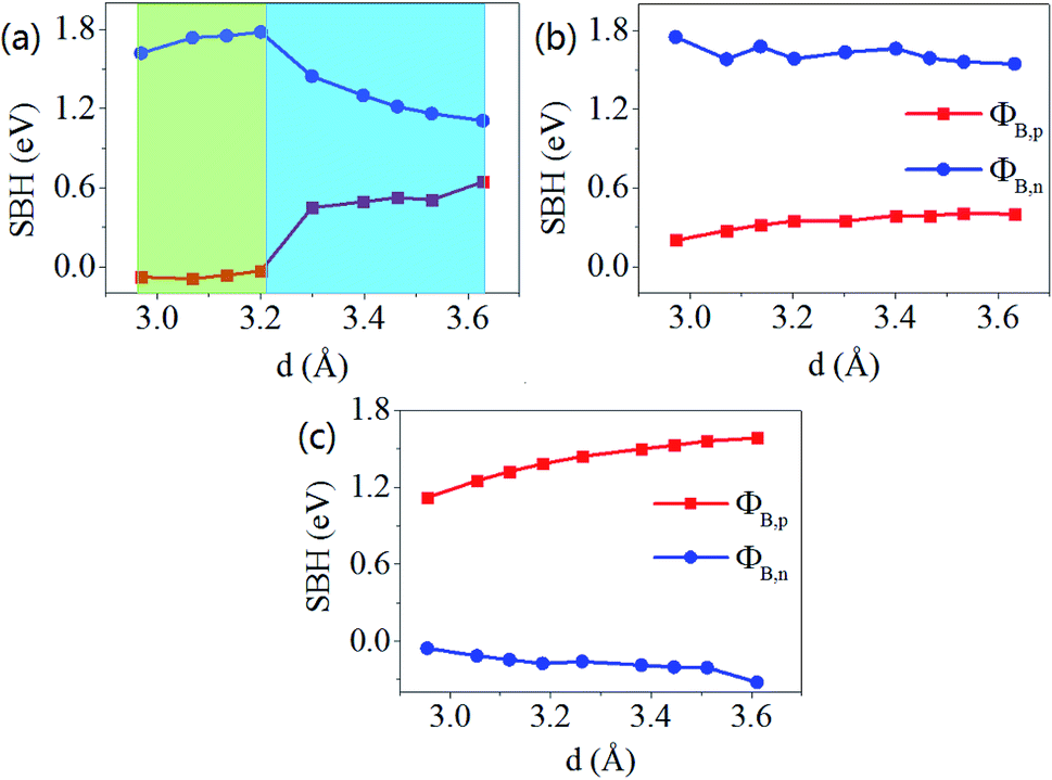 | ||
| Fig. 5 The evolution of the Schottky barrier as a function of the interlayer distance for graphene/g-GaN (a), graphene/g-GaN-VGa (b), and graphene/g-GaN-VN (c). | ||
To better understand the variations in SBH with d in graphene/g-GaN with or without defects, the xy-averaged electrostatic potential in the z direction was calculated, as shown in Fig. 6. In the graphene/g-GaN heterostructure, the system is p-type Schottky contact when d = 3.629 Å. As d decreases, the effect of interlayer coupling between the two sublayers becomes stronger, and more electrons move from graphene to g-GaN, which downward shifts the energy level of graphene close to the VBM of g-GaN, thereby decreasing the p-type SBH, resulting in a transition from a p-type Schottky contact to an ohmic contact at the interface (Fig. 6(a)). The same idea can also be applied to the graphene/g-GaN-VGa heterostructure (Fig. 6(b)). As can be seen from Fig. 6(c), it is evident that more electrons are transferred from GaN-VN to graphene as d decreases from 3.611 Å to 2.969 Å, which moves the energy level of graphene from the VBM down to the CBM of the GaN-VN sublayer, eventually causing the transition from an ohmic contact to a nearly n-type Schottky contact at the interface.
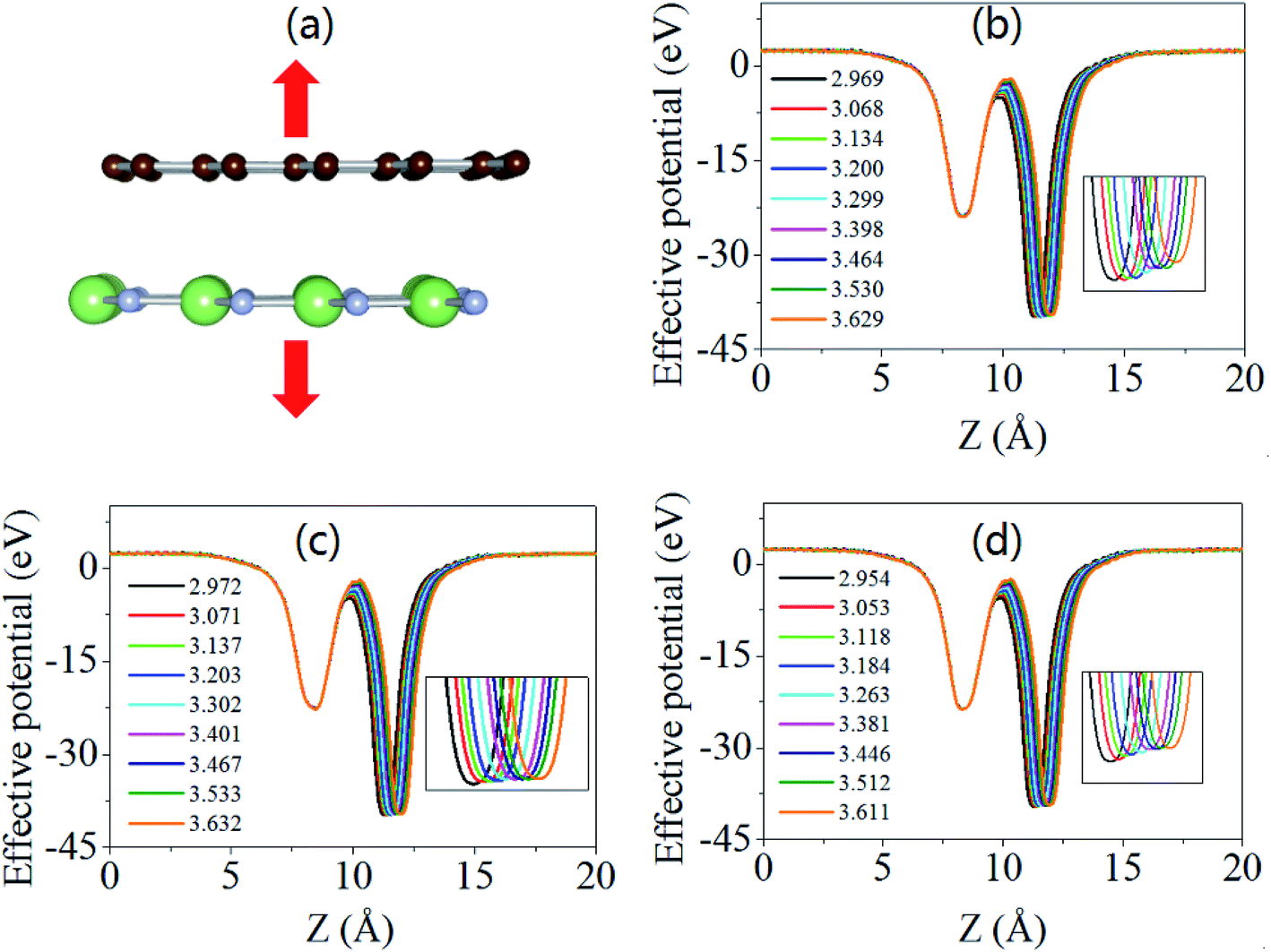 | ||
| Fig. 6 A schematic diagram of vdW heterostructures with out-of-plane strain (a), and the electrostatic potential of graphene/g-GaN (b), graphene/g-GaN-VGa (c), and graphene/g-GaN-VN with various interlayer distances (d). | ||
In addition, it should be noted that, although it is still challenging to change the interlayer distance between graphene and g-GaN in the heterostructures experimentally, some research groups have been exploring how the interlayer distance of 2D layered-material systems could be tuned effectively in practice. For example, Tongay et al. experimentally demonstrated that the interlayer distance (coupling) of WS2/MoS2 heterostructures can be tuned by vacuum thermal annealing.46 Therefore, out-of-plane strain may be experimentally applied in a graphene/g-GaN heterostructure by means of vacuum thermal annealing in the near future, which will further affect the Schottky barrier and related electronic characteristics of graphene/g-GaN-based electronic devices.
4. Conclusions
Systematic first-principles calculations were performed to understand the effects of structural imperfections on the electronic properties of graphene/g-GaN heterostructures. The findings can be summarized as follows:(1) There is weak interaction between graphene and g-GaN with or without defects via vdW forces.
(2) The graphene/g-GaN heterostructure is a p-type Schottky contact with an SBH of 0.499 eV. The graphene/g-GaN-VGa heterostructure is still a p-type Schottky contact in the spin-up channel. However, the SBH is decreased to 0.332 eV. However, the graphene/g-GaN-VN heterostructure has become an ohmic contact with a negative value for ΦB,n.
(3) The large potential drop between graphene and g-GaN implies that a lower charge-injection barrier is formed at the interface. Moreover, the introduction of Ga vacancies in g-GaN can further lower the barrier at the graphene/g-GaN interface, resulting in better device performance.
(4) By varying the interlayer distance, the SBH in the graphene/g-GaN heterostructure can be effectively modulated. Interestingly, for the graphene/g-GaN-VN heterostructure, the ohmic contact remains with various interlayer distances.
Conflicts of interest
There are no conflicts to declare.Acknowledgements
This research was supported by the National Natural Science Foundation of China (Grant No. 51274163 and 51605146), the Key Program of the National Natural Science Foundation of China (Grant No. U1502274), and the Key Science and Technology of Henan Province (Grant No. 172102410046).References
- K. S. Novoselov, A. K. Geim, S. V. Morozov, D. Jiang, Y. Zhang, S. V. Dubons, I. V. Grigorieva and A. A. Firsov, Science, 2004, 306, 666–669 CrossRef CAS PubMed.
- A. K. Geim and K. S. Novoselov, Nat. Mater., 2007, 6, 183 CrossRef CAS PubMed.
- K. Watanable, T. Taniguchi and H. Kanda, Nat. Mater., 2004, 3, 404 CrossRef PubMed.
- Q. L. Fang, X. M. Zhao, Y. H. Huang, K. W. Xu, T. Min, P. K. Chu and F. Ma, Phys. Chem. Chem. Phys., 2018, 20, 553 RSC.
- B. Radisavljevic, A. Radenovic, J. Brivio, V. Giacometti and A. Kis, Nat. Nanotechnol., 2011, 6, 147 CrossRef CAS PubMed.
- Q. L. Fang, Y. H. Huang, Y. P. Miao, K. W. Xu, Y. Li and F. Ma, J. Phys. Chem. C, 2017, 121, 6605 CrossRef CAS.
- H. Liu, A. T. Neal and Z. Zhu, ACS Nano, 2014, 8, 4033 CrossRef CAS PubMed.
- R. Fei and Y. Li, Nano Lett., 2014, 14, 2884 CrossRef CAS PubMed.
- D. B. Farmer, H. Y. Chiu, Y. M. Lin, K. A. Jenkins, F. N. Xia and P. Avouris, Nano Lett., 2009, 9, 4474 CrossRef CAS PubMed.
- Y. B. Zhang, Y. W. Tan, H. L. Stormer and P. Kim, Nature, 2005, 438, 201 CrossRef CAS PubMed.
- M. Spinkle, D. Siegel, Y. Hu, J. Hicks, A. Tejeda, A. Tableb-Ibrahimi, P. Le Fevre, F. Bertran, S. Vizzini, H. Enriquez, S. Chiang, P. Soukiassian, C. Berger, W. A. de Heer, A. Lanzara and E. H. Conrad, Phys. Rev. Lett., 2009, 103, 226803 CrossRef PubMed.
- Y. Q. Wu, Y. M. Lin, A. A. Bol, K. A. Jenkins, F. N. Xia, D. B. Farmer, Y. Zhu and P. Avouris, Nature, 2011, 472, 74–78 CrossRef CAS PubMed.
- Q. L. Fang, X. M. Zhao, Y. H. Huang, K. W. Xu, T. Min, P. K. Chu and F. Ma, J. Mater. Chem. C, 2018, 6, 4523 RSC.
- Y. Q. Zhao, Q. R. Ma, B. Liu, Z. L. Yu, J. L. Yang and M. Q. Cai, Nanoscale, 2018, 10, 8677 RSC.
- Y. Q. Zhao, X. Wang, B. Liu, Z. L. Yu, P. B. He, Q. Wang, M. Q. Cai and H. L. Yu, Org. Electron., 2018, 53, 50 CrossRef CAS.
- Z. L. Yu, Q. R. Ma, Y. Q. Zhao, B. Liu and M. Q. Cai, J. Phys. Chem. C, 2018, 122, 9275 CrossRef CAS.
- Q. L. Fang, X. M. Zhao, Y. H. Huang, K. W. Xu, T. Min and F. Ma, J. Mater. Chem. C, 2019, 7, 3607 RSC.
- X. Z. Deng, Q. Q. Zhao, Y. Q. Zhao and M. Q. Cai, Curr. Appl. Phys., 2019, 19, 279 CrossRef.
- B. Liu, Y. Q. Zhao, Z. L. Yu, L. Z. Wang and M. Q. Cai, J. Colloid Interface Sci., 2018, 513, 667 Search PubMed.
- J. Padilha, A. Fazzio and A. J. da Silva, Phys. Rev. Lett., 2015, 114, 066803 CrossRef CAS PubMed.
- H. V. Phuc, N. N. Hieu, B. D. Hoi, L. T. Phuong and C. V. Nguyen, Surf. Sci., 2018, 668, 23 CrossRef CAS.
- K. Chung, C. H. Lee and G. C. Yi, Science, 2010, 330, 655 CrossRef CAS PubMed.
- H. J. Tian, Q. L. Liu, A. Q. Hu, X. Y. He, Z. H. Hu and X. Guo, Opt. Express, 2018, 26, 5408 CrossRef CAS PubMed.
- H. J. Zhaong, Z. H. Liu, L. Shi, G. Z. Xu, Y. M. Fan, Z. L. Huang, J. F. Wang, G. Q. Ren and K. Xu, Appl. Phys. Lett., 2014, 104, 212101 CrossRef.
- D. Lioyd, X. H. Liu, J. W. Christopher, L. Cantley, A. Wadehra, B. L. Kim, B. B. Goldberg, A. K. Swan and J. S. Bunch, Nano Lett., 2016, 16, 5836 CrossRef PubMed.
- K. D. Pham, N. N. Hieu, H. V. Phuc, I. A. Fedorov, C. A. Duque, B. Amin and C. V. Nguyen, Appl. Phys. Lett., 2018, 113, 171605 CrossRef.
- M. L. Sun, J. P. Chou, Q. Q. Ren, Y. M. Zhao, J. Yu and W. C. Tang, Appl. Phys. Lett., 2017, 110, 173105 CrossRef.
- L. Huang, Q. Yue, J. Kang, Y. Li and J. B. Li, J. Phys.: Condens. Matter, 2014, 26, 295304 CrossRef PubMed.
- G. Kresse and J. Hafner, Phys. Rev. B: Condens. Matter Mater. Phys., 1993, 47, 558 CrossRef CAS.
- G. Kresse and J. Hafner, Phys. Rev. B: Condens. Matter Mater. Phys., 1994, 49, 14251 CrossRef CAS.
- P. E. Blöchl, Phys. Rev. B: Condens. Matter Mater. Phys., 1994, 50, 17953 CrossRef.
- J. P. Perdew, K. Burke and M. Ernzerhof, Phys. Rev. Lett., 1996, 77, 3865–3868 CrossRef CAS PubMed.
- Q. Chen, H. Hu, X. J. Chen and J. L. Wang, Appl. Phys. Lett., 2011, 98, 053102 CrossRef.
- S. Grimme, J. Comput. Chem., 2006, 27, 1787 CrossRef CAS PubMed.
- K. Momma and F. Izumi, J. Appl. Crystallogr., 2008, 41, 653–658 CrossRef CAS.
- L. Liu, P. Jewook, A. S. Devid, F. M. Kevin, W. C. Kendal, W. Deng, B. Leonardo, C. I. Juan, A. P. Li and G. Gu, Science, 2014, 343, 163 CrossRef CAS PubMed.
- K. S. Arunima and G. H. Richard, Appl. Phys. Lett., 2014, 105, 051604 CrossRef.
- N. J. Huo, J. H. Yang, L. Huang, Z. M. Wei, S. S. Li, S. H. Wei and J. B. Li, Small, 2015, 11, 5430 CrossRef CAS PubMed.
- G. C. Constantinescu and N. D. M. Hine, Phys. Rev. B: Condens. Matter Mater. Phys., 2015, 91, 195416 CrossRef.
- Y. X. Deng, Z. Luo, N. J. Conrad, H. Liu, Y. J. Gong, S. Najmaei, P. M. Ajayan, J. Lou, X. F. Xu and P. D. Ye, ACS Nano, 2014, 8, 8292 CrossRef CAS PubMed.
- T. Roy, M. Tosun, X. Cao, H. Fang, D. H. Lien, P. D. Zhao, Y. Z. Chen, Y. L. Chueh, J. Guo and A. Javey, ACS Nano, 2015, 114, 066803 Search PubMed.
- X. Lin, Y. Xu, A. A. Hakro, T. Hasan, R. Hao, B. L. Zhang and H. S. Chen, J. Mater. Chem. C, 2013, 1, 1618 RSC.
- W. Hu, Z. Li and J. Yang, J. Chem. Phys., 2013, 139, 154704 CrossRef PubMed.
- J. J. Guo, Z. P. Zhou, T. X. Wang, Z. S. Lu, Z. X. Yang and C. Liu, Curr. Appl. Phys., 2017, 17, 1714 CrossRef.
- M. L. Sun, J. P. Chou, Q. Q. Ren, Y. M. Zhao, J. Yu and W. C. Tang, Appl. Phys. Lett., 2017, 110, 173105 CrossRef.
- S. Tongay, W. Fan, J. Kang, J. Park, U. Koldemir, J. Suh, D. S. Narang, K. Liu, J. Ji, J. Li, R. Sinclair and J. Wu, Nano Lett., 2014, 12, 3185 CrossRef PubMed.
| This journal is © The Royal Society of Chemistry 2019 |