DOI:
10.1039/C9RA01025D
(Paper)
RSC Adv., 2019,
9, 13664-13676
Promotional effect of silver nanoparticle embedded Ga–Zr-codoped TiO2 as an alternative anode for efficient blue, green and red PHOLEDs†
Received
8th February 2019
, Accepted 24th April 2019
First published on 3rd May 2019
1. Introduction
Over the past three decades increasing attention has been paid to applied research in OLEDs due to their potential application in flat-panel displays. The efficiencies of OLEDs can be influenced by the electrodes, constituent materials and interfaces.1 The hole injection barrier (HIB) in the device ITO/NPB/Alq3/LiF/Al is ≈ 0.6 eV; because of dissociation of metal fluoride, the cathode interface barrier does not exist.2,3 In bare ITO anode devices, the energy barrier between ITO and the hole injection layer (NPB) is high resulting in fewer holes being injected. The balanced injected carriers could enhance exciton formation and improving the luminous efficiency (ηc) of the device. Due to the buffer layer at the ITO:NPB interface accumulation of holes at the interface results in effective recombination and improved efficiencies: the LiF coating between the cathode and ETL enhanced the electron injection from the cathode resulting in excellent performances.4,5 A wide band gap metal oxide semiconductor used as the hole buffer layer (HBL) (HBL; Si3N4,5 SiO2,6 Al2O3,7 MoO3,8 WO3,9 Pr2O3,10 NiO,11 Teflon,12 Ta2O5,13 TiO2 (ref. 14 and 15) etc.) was inserted between ITO and HTL in the interface. The modified ITO surface enhanced the hole injection which promoted the balanced recombination and improved the efficiencies. The operating voltage of OLEDs decreased significantly with increased luminous efficiency (ηc) by using TiO2 as the HIB.15
Though ITO is chemically unstable, harmful to human and unsuitable with flexible substrates, there is increasing demand of ITO because of its utility in various electronic devices. Therefore, efforts have been made for developing indium-free transparent conducting oxides which should exhibit comparable properties as that of ITO. The electrical resistivity of TiO2 thin film can be further improved by doping with B3+, Ga3+, and Al3+: replacing Ti4+ ions in a TiO2 crystal lattice provide an extra electron16–18 which enhanced the optoelectronic properties comparable to that of ITO.19,20 Gallium doped TiO2 thin film with close Ga–O (1.92 Å) and Ti–O (1.86 Å) bond length in Ga-doped TiO2 exhibit high electrochemical stability with minimized crystal. The smooth surface attributed by surfactant effect of Ga3+ (74.5 pm) doping in TiO2 is beneficial for the development of OLED applications.18,20 Compared with group III elements, Zr-doped TiO2 exhibits increasing thin film conductivity: Zr and Ti are having same valence state (4+) with similar atom semidiameters (Ti-2.00 Å; Zr-2.16 Å): both semiconductors are n-type with almost identical properties. Therefore, it is possible for substitution of Ti atom by Zr atom in TiO2 lattice which introduce lattice defects and Zr-doped TiO2 possess high thermo-stabilizing properties.21 Therefore, we aimed to synthesize Ga–Zr-codoped TiO2 for OLED applications. The surface-plasmon of noble-metal nanostructures enhanced the optoelectronic device efficiencies.22–37 The OLED efficiency have been increased by reducing the hole injection barrier through embedding noble-metal nano semiconductors. The interface have been stabilized via tuning HIL38–41 by forming electrical double layer on anode that stabilized the vacuum level.38 To our knowledge is concern, only few reports about efficient red, green and blue OLEDs with TiO2 as cost effective anode material instead of ITO. We aimed to combine the advantages of Ga and Zr elemental doping of TiO2 as a high performance Ga–Zr-codoped TiO2 nanoparticles for OLED applications. We report the efficient red (R), green (G) and blue (B) phosphorescent OLEDs using silver nanoparticles sandwiched between Ga–Zr-codoped TiO2 NPs and glass substrate with Ir(bbt)2(acac), Ir(tfpdni)2(pic) and Ir(fni)3 as red, green and blue emitters, respectively.
2. Experimental
2.1. Characterization
The structure of red, green and blue emitters emissive materials namely Ir(bbt)2(acac), Ir(tfpdni)2(pic) and Ir(fni)3 was confirmed with 1H and 13C NMR and mass spectra, using Bruker 400 MHz spectrometer and Agilent LCMS VL SD, respectively. Potentials were determined from CHI 630A potentiostat electrochemical analyzer. Optical absorption studies were made bu using Lambda 35 PerkinElmer and Lambda 35 spectrophotometer with integrated sphere (RSA-PE-20) instrument. PerkinElmer LS55 fluorescence spectrometer measurement was employed to study emission characteristics. Thermal characteristics of the materials were analysed with decomposition (Td) and glass transition (Tg) temperatures recorded with PerkinElmer thermal analysis system (10 °C min−1; N2 flow rate – 100 ml min−1) and NETZSCH (DSC-204) (10 °C min−1 under N2 atmosphere) instruments, respectively. XPS of nanomaterials were recorded with X-ray photoelectron spectra: ESCA−3 Mark II spectrometer-VG – Al Kα (1486.6 eV) radiation. SEM (scanning electron microscopic images) images and EDS (energy dispersive X-ray spectra) of nanomaterials were recorded by using JEOL JSM-5610 equipped with back electron (BE) detector and FEI Quanta FEG, respectively. The TEM (transmission electron microscopy) image of nanomaterials was obtained from Philips TEM with 200 kV electron beam and SAED (selected area electron diffraction) pattern was obtained from Philips TEM (CCD camera; 200 kV). The XRD of nanomaterials was recorded using Equinox 1000 diffractometer (Cu Kα rays; 1.5406 Å; current – 30 mA; 40 kV).
2.2. Fabrication of HyLEDs
The newly synthesized iridium(III) complexes namely, Ir(bbt)2(acac), Ir(tfpdni)2(pic) and Ir(fni)3 are employed as red, green and blue emitters, respectively. The fabricated OLEDs are having the following configuration: glass/Ag (2 nm)/Ga–Zr-codoped TiO2 (60 nm)/NPB (40 nm)/CBP:Ir(fni)3 (25 nm)/LiF (1 nm)/Al (100 nm) (I); glass/Ag (2 nm)/Ga–Zr-codoped TiO2 (60 nm)/NPB (40 nm)/CBP:Ir(bbt)2(acac) (25 nm)/LiF (1 nm)/Al (100 nm) (III) and glass/Ag (2 nm)/Ga–Zr-codoped TiO2 (60 nm)/NPB (40 nm)/CBP:Ir(tfpdni)2(pic) (25 nm)/LiF (1 nm)/Al (100 nm) (IV). The reference devices with the configuration of ITO/NPB (40 nm)/CBP:Ir(fni)3 (25 nm)/LiF (1 nm)/Al (100 nm) (II); ITO/NPB (40 nm)/CBP:Ir(bbt)2(acac) (25 nm)/LiF (1 nm)/Al (100 nm) (IV) and ITO/NPB (40 nm)/CBP:Ir(tfpdni)2(pic) (25 nm)/LiF (1 nm)/Al (100 nm) (VI) have been fabricated. The fabrication was made by using vacuum deposition (5 × 10⁻⁶ torr) over ITO-coated glass with 20 Ω per square resistance. Organic substances deposition was made on the ITO glass substrates with a rate of 1–2 Å s−1 and LiF was evaporated thermally over organic surface. The EL spectra, luminance characteristics and CIE coordinates measured with recorded with USB-650-VIS-NIR spectrometer (Ocean Optics, Inc, USA). Thickness was determined with quartz crystal thickness monitor and current density (J)–voltage (V) and luminescence (L)–voltage (V) studies were performed using Keithley 2400 source meter.
2.3. Synthesis of Ga–Zr-codoped TiO2
To titanium isopropoxide (1.15 g) in 25 ml methoxy ethanol solution, a mixture of gallium nitrate (1.15 g) and zirconium nitrate (1.15 g) was added. The solution was stirred at 150 °C for 1 h. The sol was after cooling which was dried at 180 °C for 24 h and calcinated (at 500 °C: 6 h: heating rate 10 °C min−1).42,43
2.4. Synthesis of silver nanoparticles (Ag NPs)
The M. elengi fruit pericarp powder was extracted with water and filtered through 0.22 μm cellulose nitrate membrane filter paper. The extract was stirred with aqueous 10 ml 0.01 M AgNO3 at 60 °C for 1 h and Ag NPs solution was stored at 5 °C.44
2.5. Synthesis of 2-(4-(trifluoromethyl)phenyl)-4,5-dimethyl-1-(naphthalen-1-yl)-1H-imidazole (tfpdni)
A mixture of butane-2,3-dione (1 mmol), 4-(trifluoromethyl)benzaldehyde (1 mmol), naphthalen-1-amine (1 mmol) and ammonium acetate (1 mmol) in acetic acid (20 ml) was refluxed (80 °C; 24 h; under N2). After cooling, the reaction mixture was extracted with dichloromethane and column chromatographed using benzene![[thin space (1/6-em)]](https://www.rsc.org/images/entities/char_2009.gif) :ethyl acetate (9:1) as the eluent (Scheme 1). Yield: 63%. Anal. calcd. for C22H17F3N2: C, 72.12; H, 4.68; N, 7.65. Found: C, 71.92; H, 4.23; N, 7.15. 1H NMR (400 MHz, CDCl3): δ 2.28 (s, 6H), 7.34 (m, 4H), 7.43–7.41 (d, 2H), 7.52 (d, 2H), 7.78 (m, 3H). 13C NMR (100 MHz, CDCl3): 4.9, 11.8, 123.82, 124.23, 125.53, 127.37, 127.96, 131.08, 132.49, 134.61, 144.58. MS: m/z. 366.13 [M+] calcd. 364.12.
:ethyl acetate (9:1) as the eluent (Scheme 1). Yield: 63%. Anal. calcd. for C22H17F3N2: C, 72.12; H, 4.68; N, 7.65. Found: C, 71.92; H, 4.23; N, 7.15. 1H NMR (400 MHz, CDCl3): δ 2.28 (s, 6H), 7.34 (m, 4H), 7.43–7.41 (d, 2H), 7.52 (d, 2H), 7.78 (m, 3H). 13C NMR (100 MHz, CDCl3): 4.9, 11.8, 123.82, 124.23, 125.53, 127.37, 127.96, 131.08, 132.49, 134.61, 144.58. MS: m/z. 366.13 [M+] calcd. 364.12.
 |
| | Scheme 1 Synthetic route of Ir(fni)3, Ir(tfpdni)2(pic) and Ir(bbt)2(acac). | |
2.6. Synthesis of iridium(III)-bis(E)-2-(4-(trifluoromethyl)phenyl)-4,5-dimethyl-1-(naphthalen-1-yl)-1H-imidazole-N,C2 picolinate [Ir(tfpdni)2(pic)]
The tfpdni (2.2 mmol) and iridium(III) chloride trihydrate (1 mmol) in 2-ethoxyethanol:H2O (3:1) was refluxed at 120 °C under N2 stream. After cooling the precipitated dimer was purified with hexane washings. The dimer (1 mmol) was treated with picolinic acid (2.2 mmol) and potassium carbonate (2.5 mmol) in 2-ethoxyethanol (15 ml) and refluxed at 120 °C under nitrogen stream.45 The filtered picolinate iridium(III) complex Ir(tfpdni)2(pic) was purified by washings and the purity of Ir(tfpdni)2(pic) complex was checked by HPLC analysis (Fig. S1†) and used as emissive layer without purification by sublimation. Yield: 58%. 1H NMR (400 MHz, CDCl3): δ 2.17 (s, 12H), 7.23 (m, 8H), 7.32 (d, 1H), 7.41 (d, 4H), 7.67 (m, 6H), 7.87 (t, 1H), 8.19 (t, 1H), 8.36 (d, 1H), 9.02 (d, 1H). 13C NMR (100 MHz, CDCl3): 4.2, 10.9, 123.32, 124.19, 124.70, 125.22, 126.27, 126.96, 127.43, 130.18, 131.19, 133.41, 138.06, 143.58, 148.53, 149.62, 173.12. MALDI-TOF MS: m/z. 1041.24 [M+]; calcd. 1041.08.
2.7. Synthesis of 2-(4-fluorostyryl)-1-(naphthalen-1-yl)-1H-imidazole (fni)
A mixture of (E)-3-(4-fluorophenyl)acrylaldehyde (1 mmol), glyoxal (1 mmol), naphthalene-1-amine (1 mmol) and ammonium acetate (1 mmol) in ethanol (20 ml) was refluxed (12 h; under N2 stream). The mixture was cooled, filtered and column chromatographed (benzene:ethyl acetate (9:1) as eluent) (Scheme 1). Yield: 65%. Anal. calcd. for C21H15FN2: C, 80.24; H, 4.81; N, 8.91. Found: C, 80.12; H, 4.45; N, 8.87. 1H NMR (400 MHz, CDCl3): δ 6.89 (s, 2H), 6.92 (d, 2H), 7.29–7.41 (m, 7H), 7.60–7.80 (m, 4H). 13C NMR (100 MHz, CDCl3): 113.82, 116.43, 125.13, 126.37, 128.26, 132.78, 133.49, 135.61, 137.08, 163.06. MS: m/z. 314.36 [M+] calcd. 312.25.
2.8. Synthesis of fac-tris[2-(4-fluorostyryl)-1-(naphthalen-1-yl)-1H-imidazolynato-C2,N1]iridium(III) [Ir(fni)3]
A mixture of 2-(4-fluorostyryl)-1-(naphthalen-1-yl)-1H-imidazole (fni) (7.83 mmol), iridium(III) trisacetylacetonate (1.56 mmol) and glycerol (9 ml) was refluxed (240 °C; N2 stream; 48 h). After cooling, the reaction mixture was extracted with dichloromethane, after evaporation the fac-isomer Ir(fni)3 complex was obtained46,47 and purified by hexane washings. The purity of the complex was checked by HPLC analysis (Fig. S1†) and used as emissive layer without purification by sublimation. Yield: 55%. 1H NMR (400 MHz, CDCl3): δ 6.90 (s, 3H), 6.92 (d, 6H), 7.20–7.32 (d, 21H), 7.40 (d, 3H), 7.60 (m, 9H).·13C NMR (100 MHz, CDCl3): 112.72, 114.43, 124.08, 125.32, 127.16, 130.68, 132.79, 134.41, 136.80, 161.26. MALDI-TOF MS: m/z. 1236.39 [M+]; calcd. 1234.30.
2.9. Synthesis of 2-(benzofuran-2-yl)benzo[d]thiazole (bbt)
To 2-aminobenzenethiol (1 mmol) in dry DMF, benzofuran-2-carboxylic acid (1 mmol) and SOCl2 (10.1 mmol) was added and refluxed at 50 °C for one day. The solvent was removed and the crude solid was washed with a saturated solution of NaHCO3, 1 N HCl and cold water. The crude was column chromatographed (hexane:ethyl acetate (7:3) as eluent). Yield: 54%. Anal. calcd. for C15H9NOS: C, 71.69; H, 3.61; N, 5.57. Found: C, 71.32; H, 3.36; N, 5.25. 1H NMR (400 MHz, CDCl3): δ 6.71 (s, 1H), 7.11–7.22 (t, 2H), 7.41–7.56 (m, 4H), 8.14 (d, 1H), 8.25 (d, 1H). 13C NMR (100 MHz, CDCl3): 102.92, 111.86, 121.27, 121.81, 123.45, 123.90, 124.54, 125.77, 135.35, 153.61, 155.48, 156.10. MS: m/z. 251.04 [M+] calcd. 249.92.
2.10. Synthesis of iridium(III)-bis-2-(benzofuran-2-yl)benzo[d]thiazole-N,C2 acetylacetonate [Ir(bbt)2(acac)]
A mixture of 2-(benzofuran-2-yl)benzo[d]thiazole (bbt) (2.2 mmol) in 2-ethoxyethanol:H2O (3:1) was refluxed with iridium(III) chloride trihydrate (1 mmol) at 120 °C under N2 stream. The formed dimer after hexane washings (1 mmol) was refluxed with ancillary ligand 1,1,1,5,5,5-hexafluoropentane-2,4-dione (2.2 mmol) and potassium carbonate (2.5 mmol) in 2-ethoxyethanol (15 ml) at 120 °C under nitrogen stream.45 The precipitated iridium(III) complex was subjected to hexane and petroleum ether washings (Scheme 1). The purity of the complex was checked by HPLC analysis (Fig. S1†) and used as emissive layer without purification by sublimation. Yield: 58%. 1H NMR (400 MHz, CDCl3): δ 1.48 (d, 1H), 1.73 (d, 1H), 4.04 (s, 2H), 5.1 (s, 1H), 7.01–7.11 (t, 3H), 7.30–7.45 (m, 8H), 8.03 (d, 2H), 8.14 (d, 2H). 13C NMR (100 MHz, CDCl3): 5.2, 65.10, 101.82, 109.96, 111.25, 120.48, 122.54, 122.90, 123.54, 124.67, 134.53, 139.63, 152.16, 154.84, 155.08. MALDI-TOF MS: m/z. 905.05 [M+]; calcd. 904.98.
3. Result and discussion
3.1. Characterisation of electron injection layer
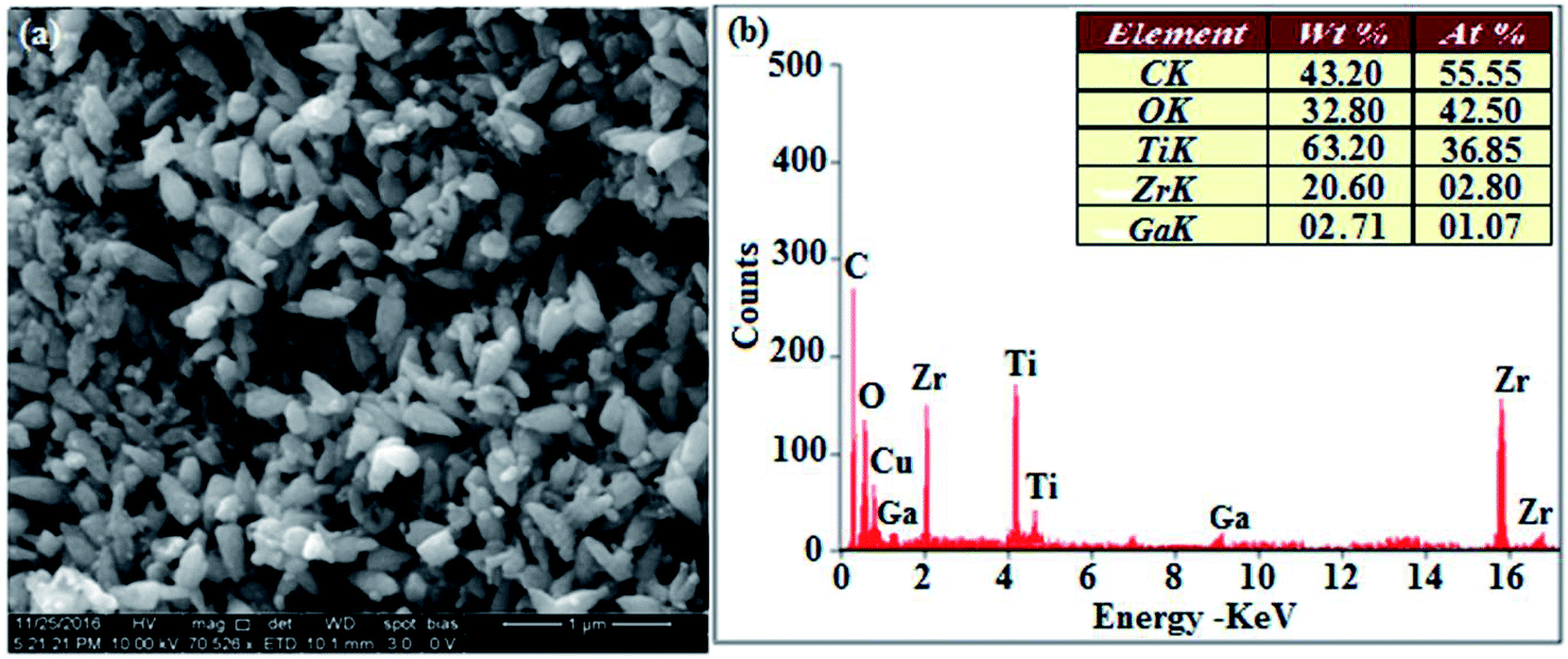
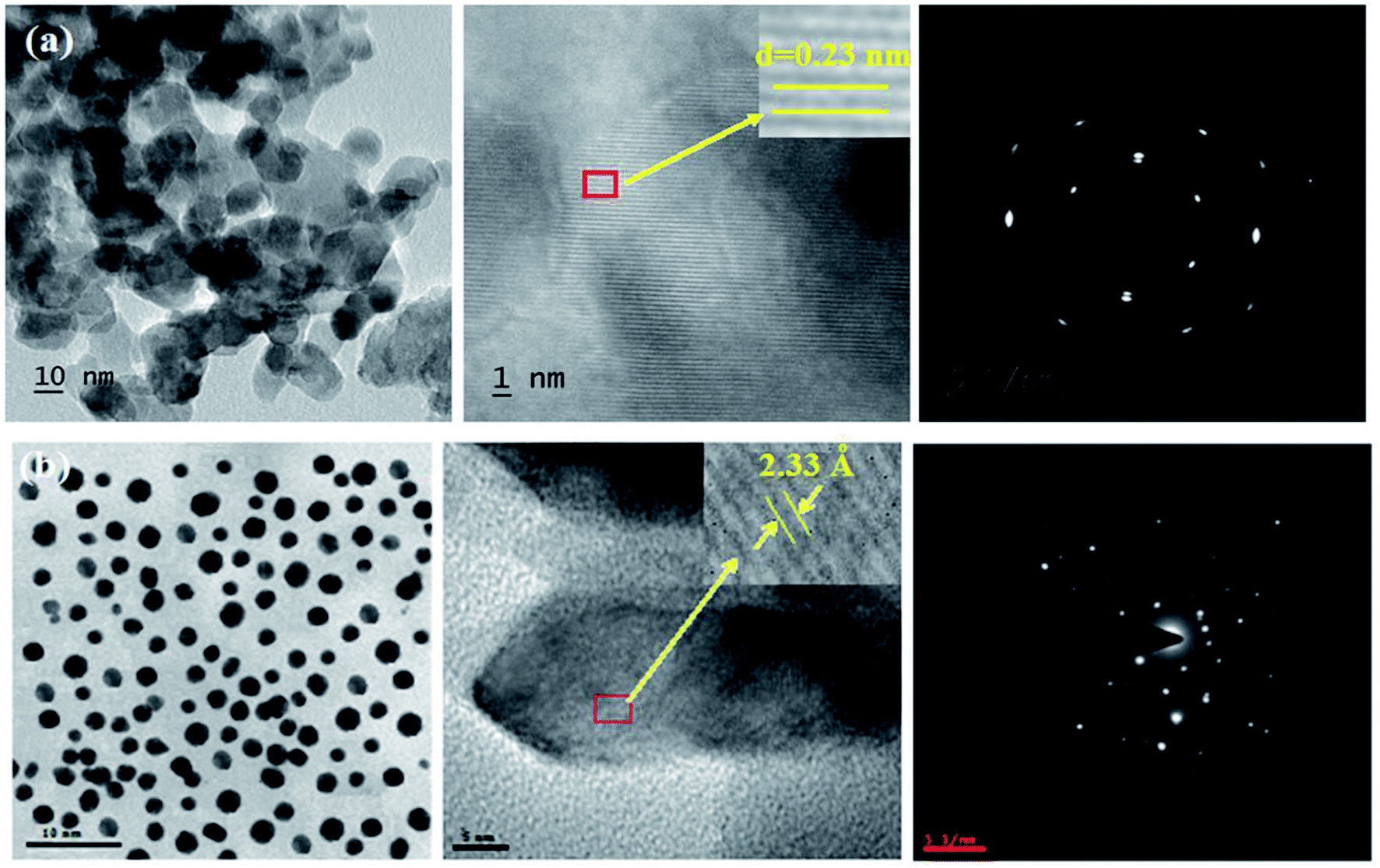
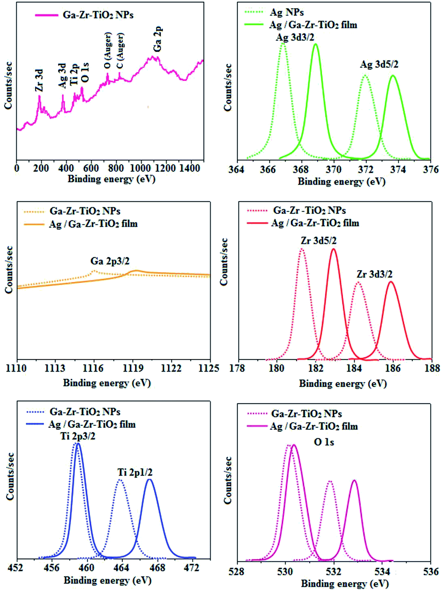
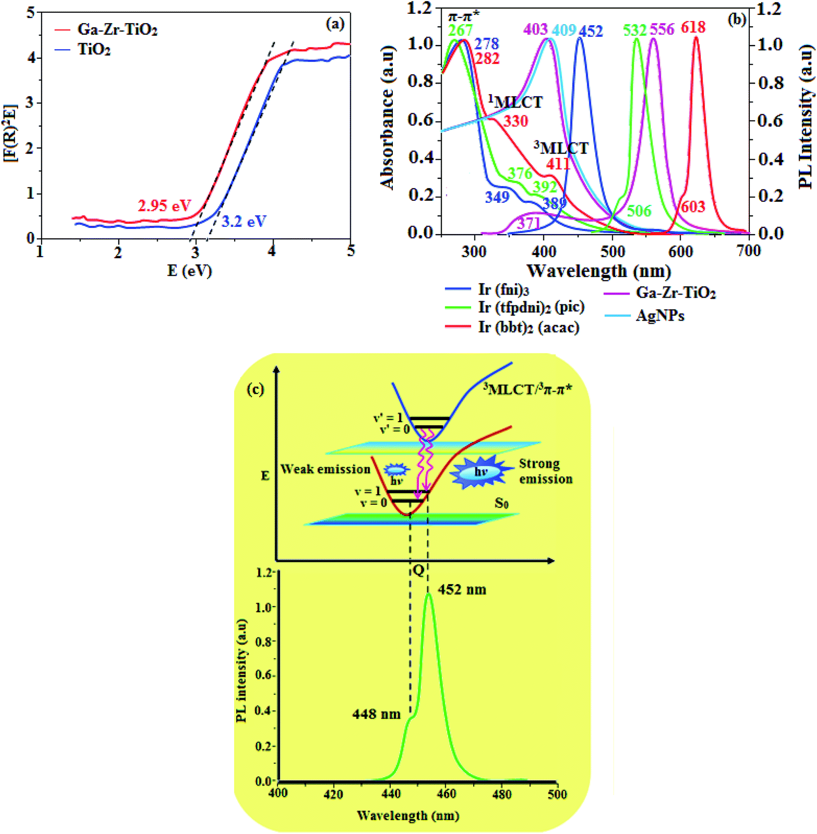
The XRD pattern of Ga–Zr-codoped TiO2 (JCPDS no. 89-4920) and Ag NPs (JCPDS no. 87-0597) is displayed in Fig. 1. The tetragonal crystal structure of Ga–Zr-codoped TiO2 with crystal constants a and b as 4.584 Å and c as 2.953 Å exhibit the intensified orientation in (110) plane. The crystal size of Ga–Zr-codoped TiO2 was deduced as 11.30 nm and surface area as 93.6 m2 g−1.46 From TEM image of Ga–Ti-codoped TiO2 the average size was estimated as 12 nm. The TEM images confirm that Ga–Zr-codoped TiO2 is nanoparticles and are approximately spherical in shape. The rings in SAED image fit with tetragonal and the TEM image shows the clear fringes with spacing of 0.24 nm corresponds with (110) plane of tetragonal TiO2. The scanning electron micrograph (SEM) of Ga–Zr-codoped TiO2 nanoparticles is displayed in Fig. 2 and the EDX of Ga–Zr-codoped TiO2 confirm the constituent elements (Fig. 2). The XRD peaks for Ag NPs at 2θ with interplanar reflections of 38.21° (1 1 1), 44.32° (2 0 0), 64.49° (2 2 0), 77.30° (3 1 1) and 81.44° (2 2 2) corresponds to face centered cubic crystal (FCC) (JCPDS no. 87-0597).47–58 The crystal size of Ag NPs is estimated as 17.32 nm and the surface area as 61.1 m2 g−1. The fringe distance 2.33 Å is calculated with spacing between (111) plane of FCC silver crystal and SAED confirm its crystalline nature. The clear diffraction circles along with bright spots in SAED pattern are identified to (111), (200), (220), (311) and (222) planes of FCC silver which is in correspondence with XRD results. The TEM images confirmed the spherical nature of Ag NPs (Fig. 3). The composition of Ga–Zr-codoped TiO2 and Ag NPs was examined by XPS which reveal Ga, Ti, Zr, O and C peaks (Fig. 4). The Gaussian peaks located at 181.3 (Zr 3d5/2) and 184.2 eV (Zr 3d3/2) and 458.8 (Ti 2p3/2) and 463.7 eV (Ti 2p1/2) confirmed Zr4+ (ref. 59) and Ti4+ (ref. 60) in Ga–Zr-codoped TiO2. The Ga 2p3/2 peak located at 1116.0 eV shows that gallium ions present as Ga3+ in Ga–Zr-codoped TiO2. Because of radii similarity, Ga3+ ions are incorporated into Ti4+ sites leading to a substitution doping.61 The signals at 530.1 (chemisorbed oxygen) and 531.8 (O2− ions in TiO2 matrix) confirmed the presence of oxygen.62,63 The 366.8 (Ag 3d5/2) and 372.0 eV (Ag 3d3/2) signals corresponds with metallic silver:64 525.0 and 530.9 eV signals reveal that O 1s profile is asymmetric in Ag NPs collected from M. elengi fruit pericarp (Fig. S2†). The composition of silver embedded Ga–Zr-codoped TiO2 film reveal that the red shifted peaks were observed for Ag, Ga, Ti, Zr, O and C on comparison with Ga–Zr-codoped TiO2 (Fig. 4). The Gaussian peaks located at 182.8 (Zr 3d5/2) and 185.9 eV (Zr 3d3/2) and 459.1 (Ti 2p3/2) and 467.0 eV (Ti 2p1/2) confirmed Zr4+ (ref. 59) and Ti4+ (ref. 60) in Ga–Zr-codoped TiO2. The Ga 2p3/2 peak located at 1119.0 eV shows Ga ions present as Ga3+ in Ga–Zr-codoped TiO2 (ref. 61) and the signals at 530.3 and 532.8 eV reveal that O 1s profile is asymmetric.62,63 The 368.9 (Ag 3d5/2) and 373.8 eV (Ag 3d3/2) signals corresponds with metallic silver.64 When the hole injection material was deposited its energy level was stabilized due to electric double layer formation and red shifted.65,66 The DRS of sol–gel synthesized Ga–Zr-codoped TiO2 presented in term of F(R) deduced from reflectance (R). The Kubelka–Munk algorithm [F(R) = (1 − R)2/2R] of Ga–Zr-codoped TiO2 is shown in Fig. 5. The absorption edge of TiO2 is 387 nm which corresponds to 3.20 eV band gap. Remarkable red shifts (420 nm) were obtained for doped Ga–Zr-codoped TiO2 thin film.67 UV-visible measurement of synthesized Ag NPs show surface plasmon absorption at 409 nm. Few percentage of co-doping effect induced shocking and causes significant red shift on comparison with single metal dopant effect.68,69 Higher absorption coefficient and well defined edge are desirable for an efficient optical absorber. The PL spectra of in Ga–Zr-codoped TiO2 show emission at 371 and 556 nm (Fig. 5).
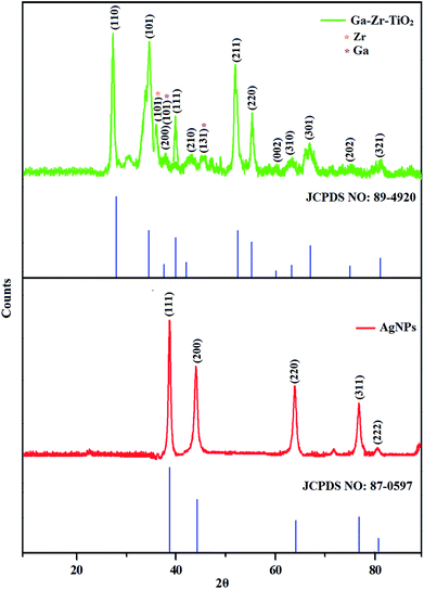 |
| | Fig. 1 X-ray diffraction pattern of Ga–Zr-codoped TiO2 (JCPDS: 89-4920) and Ag NPs (JCPDS: 87-0597). | |
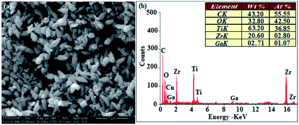 |
| | Fig. 2 HR-SEM image and EDX of Ga–Zr-TiO2. | |
 |
| | Fig. 3 HR-TEM images and SAED pattern of (a) Ga–Zr-codoped TiO2 and (b) Ag NPs. | |
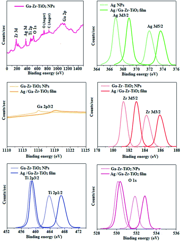 |
| | Fig. 4 X-ray photoelectron spectra (XPS) of Ga–Zr-codoped TiO2 and Ag/Ga–Zr-codoped TiO2 film. | |
 |
| | Fig. 5 (a) DRS Spectra of TiO2 and Ga–Zr-TiO2; (b) normalized absorption and emission spectra of Ir(fni)3, Ir(tfpdni)2(pic) and Ir(bbt)2(acac) and (c) Franck–Condon electronic transitions of Ir(fni)3. | |
3.2. Optical and electrochemical properties of emissive layers
The UV-vis absorption (λabs) spectra of heteroleptic iridium(III) complexes namely, Ir(fni)3, Ir(bbt)2(acac) and Ir(tfpdni)2(pic) in CH2Cl2 along with their corresponding free ligands fni, bbt and tfpdni, respectively (Fig. 5). The intensified absorption peaking of heteroleptic iridium complexes (Ir(tfpdni)2(pic) – 267 nm and Ir(bbt)2(acac) – 282 nm) is at the same energy level of free ligands bbt and tfpdni, arises from π–π* transition of cyclometalated ligands. For homoleptic complex Ir(fni)3, the absorption at 278 nm is ascribed to spin-allowed ligand-centered transition of imidazole fragment. The other two bands (Ir(tfpdni)2(pic) – 376 & 392 nm and Ir(bbt)2(acac) – 330 & 411 nm) [Ir(fni)3 – 349 & 389 nm] are assigned to MLCT transitions [1MLCT ← S0; and 3MLCT ← S0]. The intensity of 3MLCT ← S0 transition is in closest with that of 1MLCT ← S0 transition which shows that 3MLCT ← S0 transition are strongly symmetry allowed by spin–orbit coupling.70–77
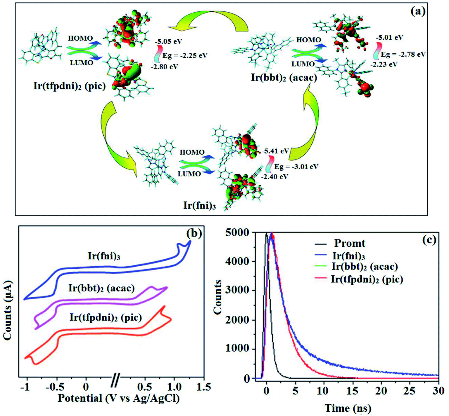
The three emissive complexes Ir(fni)3, Ir(bbt)2(acac) and Ir(tfpdni)2(pic) show strong luminescence both in solution and solid from their triplet manifold. The broad phosphorescence spectra of Ir(bbt)2(acac) and Ir(tfpdni)2(pic) show emission at 618 and 532 nm, respectively [Ir(fni)3 – 448 nm] (Fig. 5) and quantum yield (Φ) was measured as 0.68 and 0.81, respectively [Ir(fni)3 – 0.92]. The Franck–Condon-electronic transitions of emissive layer an displayed in Fig. 5 Ir(fni)3 and Ir(bbt)2(acac) and Ir(tfpdni)2(pic) in Fig. S3.† Generally, phosphorescence spectra from ligand-centered 3π–π* state is in vibronic whereas PL spectra from 3MLCT is in broad shape.78–81 Absence of vibronic emission spectra of iridium complexes [Ir(fni)3, Ir(bbt)2(acac) and Ir(tfpdni)2(pic)] supports the MLCT nature of emission which is confirmed by their phosphorescence life time of Ir(fni)3 (1.3 μs), Ir(bbt)2(acac) (1.8 μs) and Ir(tfpdni)2(pic) (2.7 μs) (Fig. 6). The broad emission spectra reveal that the excited triplet state of Ir(bpima)2(pic) and Ir(fni)3 possess dominant 3MLCT character.
 |
| | Fig. 6 (a) Frontier molecular orbital contour map; (b) cyclic voltammogram and (c) lifetime spectra of Ir(fni)3, Ir(tfpdni)2(pic) and Ir(bbt)2(acac). | |
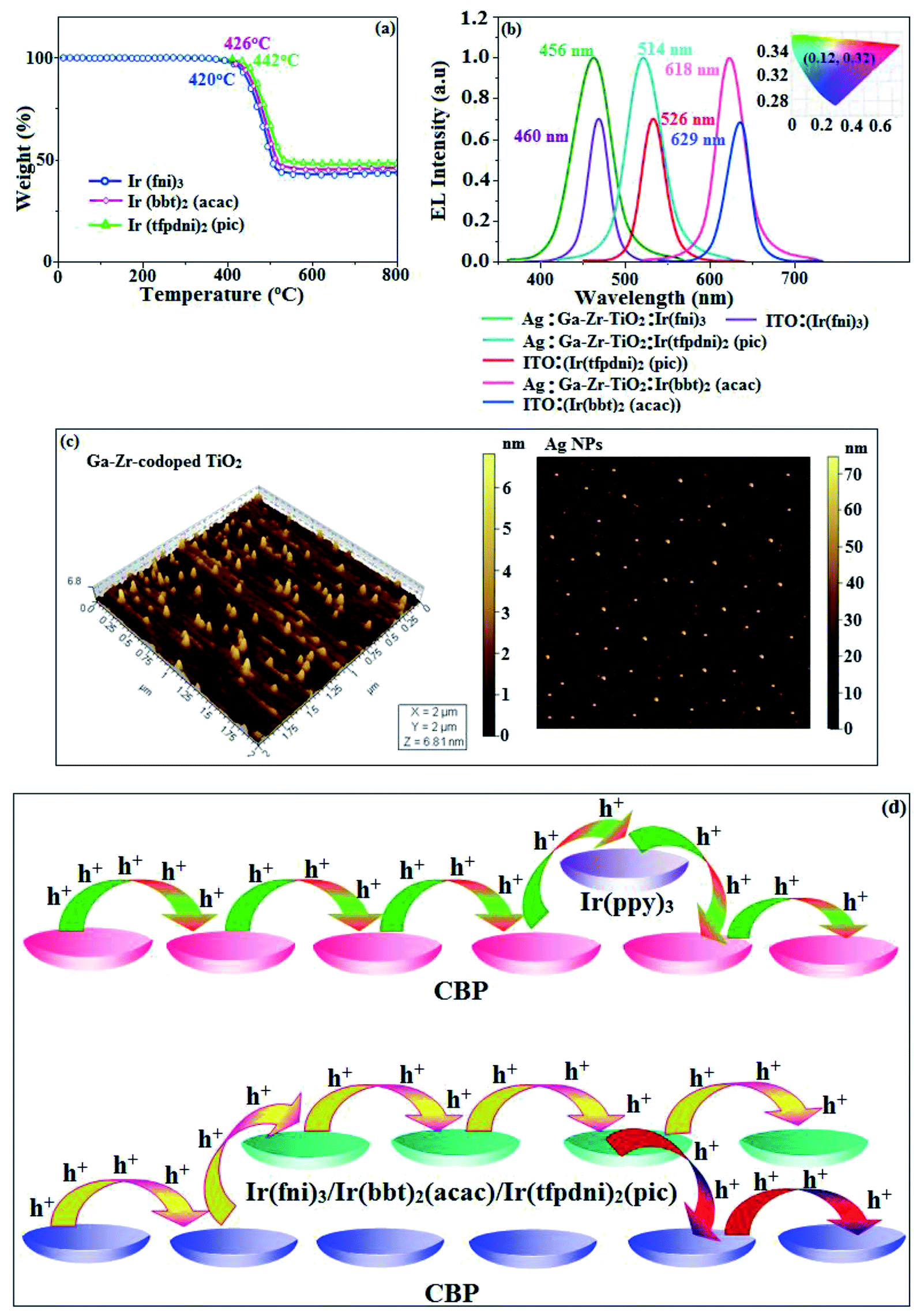
The electrochemical analysis of Ir(fni)3, Ir(bbt)2(acac) and Ir(tfpdni)2(pic) was employed with cyclic voltammetry with ferrocene/ferrocenium couple as internal reference and supporting electrolyte (0.1 M tetra(n-butyl)ammonium hexafluorophosphate: Fig. 6). The electrochemical stability of the complexes Ir(fni)3, Ir(bbt)2(acac) and Ir(tfpdni)2(pic) was confirmed by reversible one-electron oxidation wave. The HOMO energy of Ir(fni)3, Ir(bbt)2(acac) and Ir(tfpdni)2(pic) was measured as −5.41, −5.05 and −5.01 eV respectively,82 was obtained from oxidation potential and Fc/Fc+ redox couple energy [EHOMO (eV) = −(Eox + 4.8)] whereas the LUMO energy of Ir(fni)3, Ir(bbt)2(acac) and Ir(tfpdni)2(pic) was measured as −2.40, −2.80 and −2.23 eV which was deduced from ELUMO = EHOMO − 1239/λonset (Fig. 6 and Table 1). The HOMO orbital of Ir(tfpdni)2(pic) is localized on iridium, trifluoromethylbenzaldehydic and picolinate fragments whereas the LUMO orbital is majorly populated on trifluoromethylbenzaldehydic fragment. The HOMO of Ir(fni)3 is populated on iridium and fluorophenyl acrylaldehydic fragments and in LUMO the electron density is localized on naphthyl, iridium and fluorophenyl acrylaldehydic fragments. The HOMO orbital of Ir(bbt)2(acac) is majorly populated on iridium and 1,1,1,5,5,5-hexafluoropentane-2,4-dione fragments and partially on 2-aminobenzenethiol and benzofuran-2-carboxylic moieties whereas the LUMO orbital is partially populated on entire complex. The thermal characterization (Td) of Ir(fni)3, Ir(bbt)2(acac) and Ir(tfpdni)2(pic) were analyzed by TGA measurements to test its suitability for device fabrication. The TGA of Ir(fni)3, Ir(bbt)2(acac) and Ir(tfpdni)2(pic) exhibits high decomposition temperature (Td5) of 420, 442 and 426 °C, respectively (Fig. 7). The higher decomposition of blue, red and green emissive materials supports the suitability of these materials for fabrication of OLEDs and so it is expected that the synthesized iridium complexes Ir(fni)3, Ir(bbt)2(acac) and Ir(tfpdni)2(pic) will lower the turn on voltage in device performances. From the optimized geometry (Fig. 6) it was concluded that for Ir–Cav bond length is shorter than Ir–Nav bond length, Ir–Nav Ir(fni)3 (Ir–Cav – 2.02 Å < Ir–Nav – 2.10 Å), Ir(bbt)2(acac) (Ir–Cav – 2.01 Å < Ir–Nav – 2.07 Å) and Ir(tfpdni)2(pic) (Ir–Cav – 1.98 Å < Ir–Nav – 2.05 Å).80,83
Table 1 Optical and thermal properties of Ir(fni)3, Ir(bbt)2(acac) and Ir(tfpdni)2(pic)
| Parameters |
Ir(fni)3 |
Ir(tfpdni)2(pic) |
Ir(bbt)2(acac) |
| Photophysical & thermal properties |
| λab (nm) |
278349389 |
267376392 |
282330411 |
| λem (nm) |
448452 |
506532 |
603618 |
| Td5 (°C) |
420 |
426 |
442 |
| Φ |
0.92 |
0.81 |
0.68 |
| HOMO/LUMO (eV) |
−5.41/−2.40 |
−5.01/−2.23 |
−5.05/−2.80 |
| Eg (eV) |
−3.01 |
−2.78 |
−2.25 |
| τ (ns) |
1.3 |
2.7 |
1.8 |
| kr × 108 (s−1) |
7.0 |
3.0 |
3.7 |
| knr × 108 (s−1) |
0.9 |
0.7 |
1.8 |
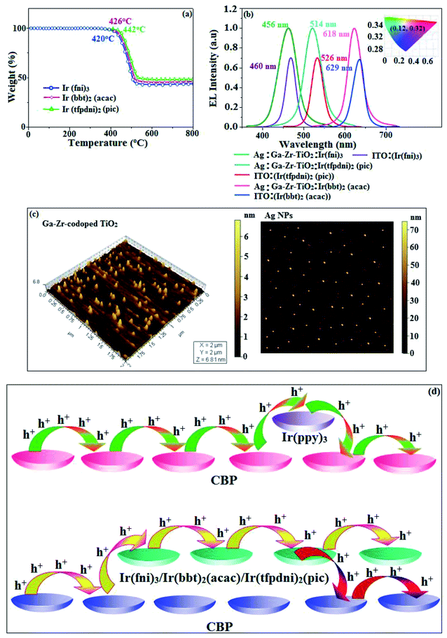 |
| | Fig. 7 (a) TGA graph; (b) EL spectra (inset: CIE coordinates); (c) AFM images of Ir(fni)3, Ir(tfpdni)2(pic) and Ir(bbt)2(acac) and (d) schematic representation of (i) carrier trapping at Ir(ppy)3 and (ii) carrier hopping through CBP and Ir(fni)3/Ir(bbt)2(acac)/Ir(tfpdni)2(pic). | |
3.3. Blue, green and red phosphorescent OLED performances
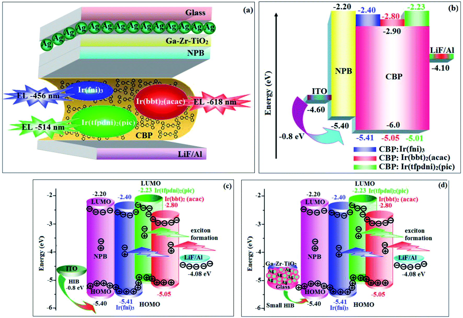
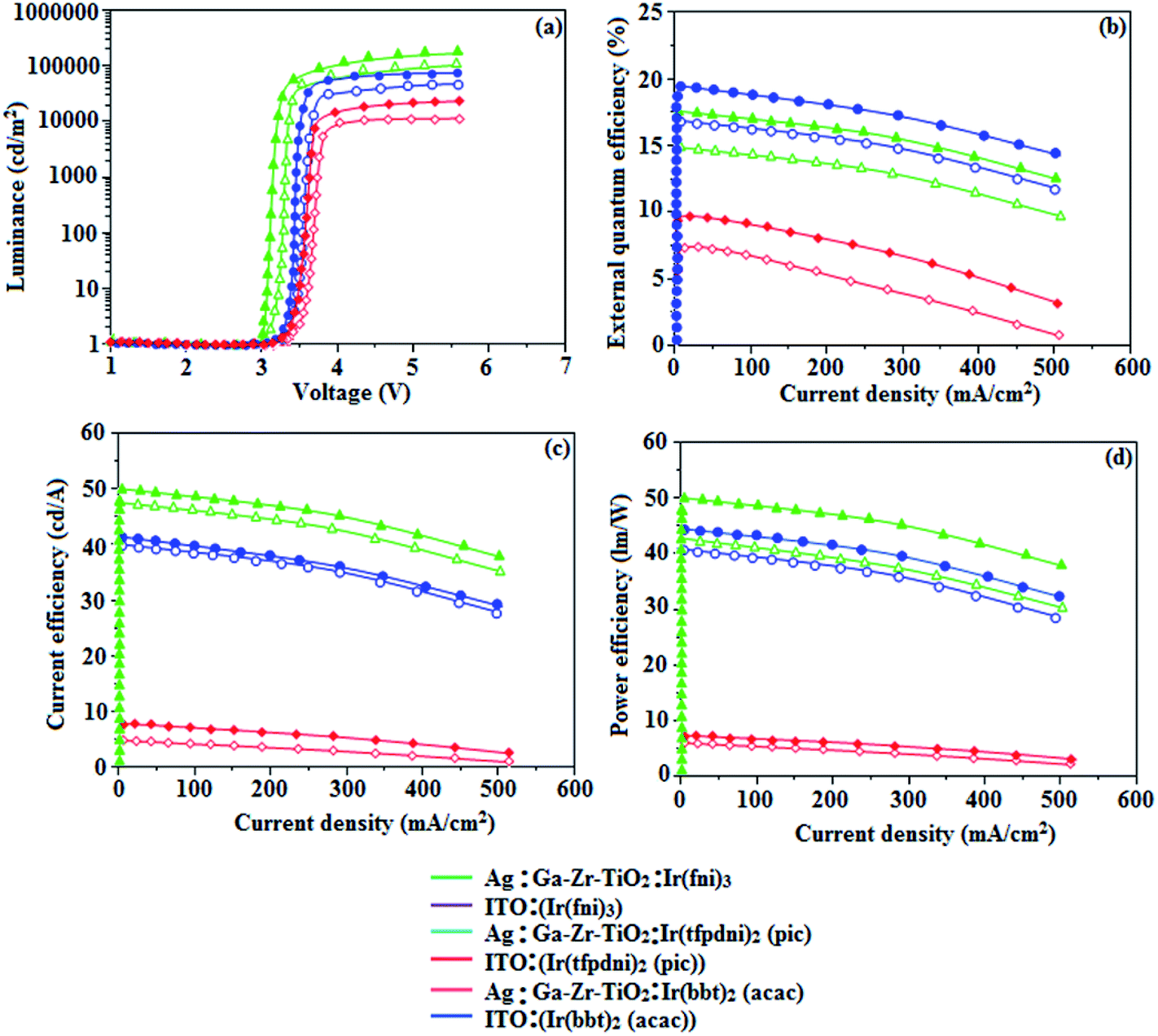
The device fabrication was made using iridium(III) complexes namely Ir(fni)3, Ir(tfpdni)2(pic) and Ir(bbt)2(acac) as blue, green and red emitters, respectively. The fabricated device structures and their energy level diagram are shown in Fig. 8. Furthermore, the N,N′-dicarbazolyl-4,4′-biphenyl (CBP) was employed as host material due to its wide energy gap and bipolar transport capability allowing balanced h+–e− recombination in the emissive layer.83,84 High triplet energy (2.3 eV) of HTM [N,N′-bis(naphthyl)-N,N′-diphenyl-1,1′-biphenyl-4,4′-diamine (NPB)] facilitates high energy exciton confinement.85–89 The RMS (2.11 nm) of silver NPS embedded Ga–Zr-codoped TiO2 is higher than ITO (Fig. 7). The Ag NPs heat conductivity is higher than ITO which induced large grains on Ga–Zr-codoped TiO2 surface. The work function (EF) of Ga–Zr-codoped TiO2 surface with Ag NPs interlayer is expected to be stabilized than EF of ITO. Hence, the interlayer of Ag NPs increase the conductivity and EF on Ga–Zr-codoped TiO2 surface results enhancing the luminance of devices (Table 2). The current density and luminance of the devices increased with the incorporation of silver nanoparticles at the interface of glass:Ga–Zr-codoped TiO2 than reference devices II, IV and VI (Fig. 9). Among the blue devices I (456 nm: Fig. 7) and II (460 nm), device I exhibit maximum luminance (L) of 40512 cd m−2 (ITO – 37623 cd m−2), current efficiency (ηc) of 41.3 cd A−1 (ITO – 40.5 cd A−1) and power efficiency (ηp) of 43.1 lm w−1 (ITO – 39.8 lm w−1) with external quantum efficiency (ηex) of 19.4% (ITO – 16.9%) at driving voltage 3.2 V. Similar observations were found for green and red devices. Newly fabricated green device with emissive layer Ir(tfpdni)2(pic) show intensified emission at 514 nm (Fig. 7) and luminance of 46435 cd m−2 (ITO – 40986 cd m−2), current efficiency (ηc) of 49.7 cd A−1 (ITO – 47.3 cd A−1), power efficiency (ηp) of 48.6 lm w−1 (ITO – 41.4 lm w−1) and external quantum efficiency (ηex) of 17.5% (ITO – 14.9%). The red device (618 nm: Fig. 7) with emissive layer Ir(bbt)2(acac) show luminance of 8936 cd m−2 (ITO – 8043 cd m−2), current efficiency (ηc) of 6.9 cd A−1 (ITO – 4.6 cd A−1), power efficiency (ηp) of 5.7 lm w−1 (ITO – 4.9 lm w−1) and external quantum efficiency (ηex) of 9.3% (ITO – 6.9%) (Fig. 9). The devices I, III and V show intensified emission than reference devices (II, IV & VI) since the hole injection barrier is reduced by stabilizing the EF by the incorporation of Ag NPs at the glass:Ga–Zr-codoped TiO2 interface results voltage reduction with intensified emission than the reference devices II, IV and VI.39 Since the embedded silver nanoparticles at glass:Ga–Zr-codoped TiO2 interface facilitate the holes to diffuse across the junction which results enhanced efficiencies: leakage of holes through emissive layer was decreased results balanced h+–e− recombination in the emissive layer and thus the nonproductive hole current was removed. The larger interface area between the emitter and HTL layer enhanced the charge injection make effective electron–hole recombination results enhanced device performances.89 Moreover the surface-plasmon enhanced emission can strongly promote the external emission of devices I, III and V. At Ga–Zr-codoped TiO2 film, Ag NPs effectively excite such emission and enhanced the device efficiencies (I, II and V). Efficient electroluminescent performances were achieved from the fabricated devices (I, III and V) with silver nanoparticles incorporation at glass:Ga–Zr-codoped TiO2 interface. In CBP:Ir(ppy)3 (25 nm) based devices the carrier current decreases sharply since the carrier may undergo deep trapping at Ir(ppy)3 HOMO orbital. However, in CBP:Ir(fni)3 (25 nm); CBP:Ir(bbt)2(acac) (25 nm); CBP:Ir(tfpdni)2(pic) (25 nm) based devices, the carrier current increased which may be attributed to the effect of direct injection into the dopant HOMO levels and the hopping transport thorough Ir(fni)3/Ir(bbt)2(acac)/Ir(tfpdni)2(pic) and dopant sites (Fig. 7). Overall, the efficiencies of the tested blue, green and red PHOLEDs indicate that the electroluminescent efficiencies of devices based on different anodes are comparable and the electroluminescent performances of OLEDs with various anodes are displayed in Table 3.85–90 The performances of the Ga–Zr-codoped TiO2-based OLEDs were not inferior to those of other previously reported efficiencies. This outstanding performance manifests the great potential of Ga–Zr-codoped TiO2 film as an alternative anode for OLEDs.
 |
| | Fig. 8 Device structure (a) glass/Ag/Ga–Zr-TiO2/NPB/CBP:Ir(fni)3 (or) CBP:Ir(bbt)2(acac) (or) CBP:Ir(tfpdni)2(pic)/LiF/Al; (b) ITO/NPB/CBP:Ir(fpi)3 (or) CBP:Ir(bbt)2(acac) (or) CBP:Ir(tfpdni)2(pic)/LiF/Al and their energy level diagrams (c) and (d). | |
Table 2 Comparative device efficiencies of Ag/Ga–Zr-TiO2 and ITO green, red and blue devices
| Device parameters |
Ir(fni)3 |
Ir(tfpdni)2(pic) |
Ir(bbt)2(acac) |
| Ag/Ga–Zr-TiO2 (I) |
ITO (II) |
Ag/Ga–Zr-TiO2 (III) |
ITO (IV) |
Ag/Ga–Zr-TiO2 (V) |
ITO (VI) |
| Von (V) |
3.2 |
3.2 |
3.0 |
3.0 |
3.3 |
3.3 |
| L (cd m−2) |
40512 |
37623 |
46435 |
40986 |
8936 |
8043 |
| ηex (%) |
19.4 |
16.9 |
17.5 |
14.9 |
9.3 |
6.9 |
| ηc (cd A−1) |
41.3 |
40.5 |
49.7 |
47.3 |
6.9 |
4.6 |
| ηp (lm W−1) |
43.1 |
39.8 |
48.6 |
41.4 |
5.7 |
4.9 |
| CIE (x, y) |
(0.15, 0.10) |
(0.16, 0.10) |
(0.12, 0.32) |
(0.12, 0.33) |
(0.68, 0.30) |
(0.68, 0.32) |
| EL (nm) |
456 |
460 |
514 |
526 |
618 |
629 |
 |
| | Fig. 9 Electroluminescence performances: (a) luminance versus voltage; (b) external quantum efficiency versus current density; (c) current efficiency versus current density and (d) power efficiency versus current density of Ir(fni)3, Ir(tfpdni)2(pic) and Ir(bbt)2(acac). | |
Table 3 External quantum efficiency of OLEDs with various anodes
| Anode |
Emissive materials/color |
EQE (%) |
Reference |
| Zr:ZnO |
Alq3/green |
0.87 |
85 |
| In:ZnO |
Fac-Ir(ppy)3/green |
13.2 |
86 |
| Ga:ZnO |
FIrpic/blue |
1.52 |
87 |
| NPs |
FIrpic/blue |
8.2 |
88 |
| Ga–Ti-ZnO |
Ir(piq)2acac/red |
9.1 |
88 |
| Fac-Ir(ppy)3/green |
14.5 |
89 |
| FIrpic/blue |
19.0 |
89 |
| Ag/Ga–Ti-ZnO |
Ir(bpima)2(pic)/blue |
19.2 |
90 |
| Ir(fpi)3/green |
15.6 |
90 |
| Ag/Ga–Zr-TiO2 |
Ir(fni)3/blue |
19.4 |
This work |
| Ir(tfpdni)2(pic)/green |
17.5 |
This work |
| Ir(bbt)2(acac)/red |
9.3 |
This work |
4. Conclusion
The coupling of surface plasmonic and hole injection ability exerted by Ag NPs enhanced the fabricated device efficiency. Enhanced efficiencies have been obtained by incorporating Ag NPs at glass:Ga–Ti-codoped TiO2 interface to avoid altering the hole mobility on Ga–Ti-codoped TiO2 surface. Among the blue devices I (456 nm) and II (460 nm), device I exhibit maximum luminance (L) of 40512 cd m−2 (ITO – 37623 cd m−2), current efficiency (ηc) of 41.3 cd A−1 (ITO – 40.5 cd A−1) and power efficiency (ηp) of 43.1 lm w−1 (ITO – 39.8 lm w−1) with external quantum efficiency (ηex) of 19.4% (ITO – 16.9%) at driving voltage 3.2 V. Similar observations were found for green and red devices. Newly fabricated green device with emissive layer Ir(tfpdni)2(pic) show intensified emission at 514 nm and luminance of 46435 cd m−2 (ITO – 40986 cd m−2), current efficiency (ηc) of 49.7 cd A−1 (ITO – 47.3 cd A−1), power efficiency (ηp) of 48.6 lm w−1 (ITO – 41.4 lm w−1) and external quantum efficiency (ηex) of 17.5% (ITO – 14.9%). The red device (618 nm) with emissive layer Ir(bbt)2(acac) show luminance of 8936 cd m−2 (ITO – 8043 cd m−2), current efficiency (ηc) of 6.9 cd A−1 (ITO – 4.6 cd A−1), power efficiency (ηp) of 5.7 lm w−1 (ITO – 4.9 lm w−1) and external quantum efficiency (ηex) of 9.3% (ITO – 6.9%). The outcome of present investigation reveals the potential advantages by the use of Ga–Zr-codoped TiO2 as an alternative OLED anode in terms of higher efficiency, low voltage and luminance. The superior characteristics of this tailored silver embedded Ga–Zr-codoped TiO2 anode points toward the replacement of ITO anodes in future OLED applications.
Conflicts of interest
There are no conflicts to declare.
Acknowledgements
One of the author Dr J. Jayabharathi thank the DST (Department of Science and Technology – EMR/2014/000094, F. No. SR/S1/1C-73/2010, F. No. SR/S1/1C-07/2007), DRDO (Defence Research and Development Organization – 213/MAT/10-11), CSIR (Council of Scientific and Industrial Research – No. 01/ (2707)/13EMR-II), UGC (University Grant Commission – 36-21/2008, F. No. 30-71/2004(SR)) and DST-Nano Mission (SR/NM/NS-1001/2016) for financial support.
References
- C. F. Qiu, Z. L. Xie, H. Y. Chen, M. Wong and H. S. Kwok, J. Appl. Phys., 2003, 93, 3253–3258 CrossRef CAS.
- S. M. Tadayyon, H. M. Grandin, K. Griffiths, P. R. Norton, H. Aziz and Z. D. Popovic, Org. Electron., 2004, 5, 157–166 CrossRef CAS.
- P. He, S. D. Wang, S. T. Lee and L. S. Hung, Appl. Phys. Lett., 2003, 82, 3218–3220 CrossRef CAS.
- L. S. Hung, C. W. Tang and M. G. Mason, Appl. Phys. Lett., 1997, 70, 152–154 CrossRef CAS.
- H. Jiang, Y. Zhou, B. S. Ooi, Y. Chen, T. Wee, Y. L. Lam, J. S. Huang and S. Y. Liu, Thin Solid Films, 2000, 363, 25–28 CrossRef CAS.
- Z. B. Deng, X. M. Ding, S. T. Lee and W. A. Gambling, Appl. Phys. Lett., 1999, 74, 2227–2229 CrossRef CAS.
- Y. Kurosaka, N. Tada, Y. Ohmori and K. Yoshino, J. Appl. Phys., 1998, 37, L798–L801 CrossRef.
- H. You, Y. F. Dai, Z. Q. Zhang and D. G. Ma, J. Appl. Phys., 2007, 101, 26105–26113 CrossRef.
- J. Li, M. Yahiro, K. Ishida, H. Yamada and K. Matsushige, Synth. Met., 2005, 151, 141–146 CrossRef CAS.
- H. C. Im, D. C. Choo, T. W. Kim, J. H. Kim, J. H. Seo and Y. K. Kim, Thin Solid Films, 2007, 515, 5099–5102 CrossRef CAS.
- C. F. Qiu, H. Y. Chen, Z. L. Xie, M. Wong and H. S. Kwok, Appl. Phys. Lett., 2002, 80, 3485–3487 CrossRef CAS.
- Y. Qiu, Y. D. Gao and L. D. Wang, Synth. Met., 2003, 130, 235–237 CrossRef.
- H. T. Lu and M. Yokoyama, Solid-State Electron., 2003, 47, 1409–1412 CrossRef CAS.
- Z. F. Zhang, Z. B. Deng and C. J. Liang, Displays, 2003, 24, 231–234 CrossRef CAS.
- Z. H. Huang, X. T. Zeng, E. T. Kang, Y. H. Fuhc and L. Lu, Surf. Coat. Technol., 2005, 198, 357–361 CrossRef CAS.
- J. Kang, H. W. Kim and C. Lee, J. Korean Phys. Soc., 2010, 56, 576–579 CrossRef CAS.
- W. S. Liu, W. K. Chen, S. Y. Wu and K. P. Hsueh, J. Am. Ceram. Soc., 2014, 97, 473–480 CrossRef CAS.
- Z. Z. Li, Z. Z. Chen, W. Huang, S. H. Chang and X. M. Ma, Appl. Surf. Sci., 2011, 257, 8486–8489 CrossRef CAS.
- H. J. Ko, Y. F. Chen, S. K. Hong, H. Wenisch, T. Yao and D. C. Look, Appl. Phys. Lett., 2000, 77, 3761–3763 CrossRef CAS.
- V. Khranovskyy, U. Grossner, V. Lazorenko, G. Lashkarev, B. G. Svensson and R. Yakimova, Superlattices Microstruct., 2006, 39, 275–281 CrossRef CAS.
-
(a) S. M. Chang and R. A. Doong, J. Phys. Chem. B, 2006, 110, 20808–20814 CrossRef CAS PubMed;
(b) J. Luka, M. Klementova, P. Bezdic, S. Bakardjieva, J. Subrt, L. Szatma, Z. Bastl and J. Jirkovsky, Appl. Catal., B, 2007, 74, 83–91 CrossRef.
- K. Okamoto, I. Niki, A. Shvartser, Y. Narukawa and M. A. Scherer, Nat. Mater., 2004, 3, 601–605 CrossRef CAS PubMed.
- M. K. Kwon, J. Y. Kim, B. H. Kim, I. K. Park, C. Y. Cho, C. C. Byeon and S. J. Park, Adv. Mater., 2008, 20, 1253–1257 CrossRef CAS.
- D. M. Koller, A. Hohenau, H. Ditlbacher, N. Galler, F. R. Aussenegg, A. Leitner, J. R. Krenn, S. Eder, S. Sax and E. J. W. List, Appl. Phys. Lett., 2008, 92, 103304–103313 CrossRef.
- S. Liu, F. Meng, W. Xie, Z. Zhang, L. Shen, C. Liu, Y. He, W. Guo and S. Ruan, Appl. Phys. Lett., 2013, 103, 233303–233304 CrossRef.
- J. H. Lee, J. H. Park, J. S. Kim, D. Y. Lee and K. Cho, Org. Electron., 2009, 10, 416–420 CrossRef CAS.
- S. Shi, V. Sadhu, R. Moubah, G. Schmerber, Q. Bao and S. R. P. Silva, J. Mater. Chem. C, 2013, 1, 1708–1712 RSC.
- F. Wang, X. Qiao, T. Xiong and D. Ma, Org. Electron., 2008, 9, 985–993 CrossRef CAS.
- X. W. Zhang, J. Zhang, L. Li, H. P. Lin, X. Y. Jiang, W. Q. Zhu and Z. L. Zhang, Synth. Met., 2010, 160, 788–790 CrossRef CAS.
- Z. Su, L. Wang, Y. Li, G. Zhang, H. Zhao, H. Yang, Y. Ma, B. Chu and W. Li, ACS Appl. Mater. Interfaces, 2013, 5, 12847–12853 CrossRef CAS PubMed.
- Y. Zhou, Y. Yuan, J. Lian, J. Zhang, H. Pang, L. Cao and X. Zhou, Chem. Phys. Lett., 2006, 427, 394–398 CrossRef CAS.
- J. Meyer, S. Hamwi, T. Bülow, H. H. Johannes, T. Riedl and W. Kowalsky, Appl. Phys. Lett., 2007, 91, 113506–113513 CrossRef.
- A. Kumar, P. Tyagi, R. Srivastava, D. S. Mehta and M. N. Kamalasanan, Appl. Phys. Lett., 2013, 102, 203304–203305 CrossRef.
- M. Tang, W. Zhu, L. Sun, J. Yu, B. Qian and T. Xiao, Synth. Met., 2015, 199, 69–73 CrossRef CAS.
- T. Kim, H. Kang, S. Jeong, D. J. Kang, C. Lee, C. H. Lee, M. K. Seo, J. Y. Lee and B. J. Kim, ACS Appl. Mater. Interfaces, 2014, 6, 16956–16965 CrossRef CAS PubMed.
- A. Kumar, R. Srivastava, D. S. Mehta and M. N. Kamalasanan, Org. Electron., 2012, 13, 1750–1755 CrossRef CAS.
- H. Choi, J. P. Lee, S. J. Ko, J. W. Jung, H. Park, S. Yoo, O. Park, J. R. Jeong, S. Park and J. Y. Kim, Nano Lett., 2013, 13, 2204–2208 CrossRef CAS PubMed.
- D. Wang, K. Yasui, M. Ozawa, K. Odoi, S. Shimamura and K. Fujita, Appl. Phys. Lett., 2013, 102, 023302–023303 CrossRef.
- M. Jung, D. M. Yoon, M. Kim, C. Kim, T. Lee, J. H. Kim, S. Lee, S. H. Lim and D. Woo, Appl. Phys. Lett., 2014, 105, 13306–13315 CrossRef.
- F. Liu and J. M. Nunzi, Org. Electron., 2012, 13, 1623–1632 CrossRef CAS.
- P. J. Jesuraj and K. Jeganathan, RSC Adv., 2015, 5, 684–689 RSC.
- Q. Deng, X. Han, Y. Gao and G. Shao, J. Appl. Phys., 2012, 112, 13523–13532 CrossRef.
- S. Ranjbar, K. Saberyan and F. Parsayan, Mater. Chem. Phys., 2018, 214, 337–344 CrossRef CAS.
- R. Vandana Rao and P. Ravi Kiran, Nano Sci. Nano Technol., 2012, 6, 28–31 Search PubMed.
- A. B. Tamayo, B. D. Alleyne, P. I. Djurovich, S. Lamansky, I. Tsyba, N. N. Ho, R. Bau and M. E. Thompson, J. Am. Chem. Soc., 2003, 125, 7377–7387 CrossRef CAS PubMed.
- A. Tsuboyama, H. Iwawaki, M. Furugori, T. Mukaide, J. Kamatani, S. Igawa, T. Moriyama, S. Miura, T. Takiguchi, S. Okada, M. Hoshino and K. Ueno, J. Am. Chem. Soc., 2003, 125, 12971–12979 CrossRef CAS.
- W. H. Eisa, Y. K. Abdel-Moneam, Y. Shaaban, A. A. Abdel-Fattah and A. M. A. Zeid, Mater. Chem. Phys., 2011, 128, 109–113 CrossRef CAS.
- Z. Wang, P. Lu, S. Chen, Z. Gao, F. Shen, W. Zhang, Y. Xu, H. S. Kwok and Y. Ma, J. Mater. Chem., 2011, 21, 5451–5456 RSC.
- H. Huang, Y. Wang, B. Wang, S. Zhuang, B. Pan, X. Yang and L. Wang, J. Mater. Chem. C, 2013, 1, 5899–5908 RSC.
- Z. Gao, Y. Liu, Z. Wang, F. Shen, H. Liu, G. Sun, L. Yao, Y. Lv, P. Lu and Y. Ma, Chem.–Eur. J., 2013, 19, 2602–2605 CrossRef CAS PubMed.
- Z. Wang, Y. Feng, H. Li, Z. Gao, X. Zhang, P. Lu, P. Chen, Y. Ma and S. Liu, Phys. Chem. Chem. Phys., 2014, 16, 10837–10843 RSC.
- Z. Gao, Z. Wang, T. Shan, Y. Liu, F. Shen, Y. Pan, H. Zhang, X. H. Lu, B. Yang and Y. Ma, Org. Electron., 2014, 15, 2667–2676 CrossRef CAS.
- V. E. Z. Lippert, Electrochemistry, 1957, 61, 962–975 Search PubMed.
- C. J. Chiang, A. Kimyonok, M. K. Etherington, G. C. Griffiths, V. Jankus, F. Turksoy and A. P. Monkman, Adv. Funct. Mater., 2013, 23, 739–746 CrossRef CAS.
- R. L. Martin, J. Chem. Phys., 2003, 118, 4775–4777 CrossRef CAS.
- I. A. Wani, J. Ganguly and T. Ahmad, Mater. Lett., 2011, 65, 520–522 CrossRef CAS.
- D. S. Sheny, D. Philip and J. Mathew, Spectrochim. Acta, Part A, 2013, 114, 267–271 CrossRef CAS PubMed.
- Z. Liu, L. Luo, Y. H. Dong, G. J. Weng and J. J. Li, J. Colloid Interface Sci., 2011, 363, 182–186 CrossRef CAS PubMed.
- X. Duana, C. Song, F. Yu, D. Yuan and X. Li, Appl. Surf. Sci., 2011, 257, 4291–4295 CrossRef.
- J. N. Kim, K. S. Shin, D. H. Kim, B. O. Park, N. K. Kim and S. H. Cho, Appl. Surf. Sci., 2003, 206, 119–128 CrossRef CAS.
- V. Bhosle, A. Tiwari and J. Narayan, J. Appl. Phys., 2006, 100, 033713–033716 CrossRef.
- M. Chen, X. Wang, Y. H. Yu, Z. L. Pei, X. D. Bai, C. Sun, R. F. Huang and L. S. Wen, Appl. Surf. Sci., 2000, 158, 134–140 CrossRef CAS.
- H. Wang, S. Baek, J. Song, J. Lee and S. Lim, Nanotechnology, 2008, 19, 75607–75616 CrossRef PubMed.
- N. Serpone, D. Lawless and R. Khairutdinov, J. Phys. Chem., 1995, 99, 16646–16654 CrossRef CAS.
- H. Ishii, K. Sugiyama, E. Ito and K. Seki, Adv. Mater., 1999, 11, 605–625 CrossRef CAS.
- A. Curioni, V. Boero and W. Andreoni, Chem. Phys. Lett., 1998, 294, 263–271 CrossRef CAS.
-
(a) B. X. Mi, P. F. Wang, M. W. Liu, H. L. Kwong, N. B. Wong, C. S. Lee and S. T. Lee, Chem. Mater., 2003, 15, 3148–3151 CrossRef CAS;
(b) J. Jayabharathi, G. Abirama Sundari, V. Thanikachalam, P. Jeeva and S. Panimozhi, RSC Adv., 2017, 7, 38923–38934 RSC.
- X. H. Xia, L. Lu, A. S. Walton, M. Ward, X. P. Han, R. Brydson, J. K. Luo and G. Shao, Acta Mater., 2012, 60, 1974–1985 CrossRef CAS.
- Q. R. Deng, X. H. Xia, M. L. Guo, Y. Gao and G. Shao, Mater. Lett., 2011, 65, 2051–2054 CrossRef CAS.
- J. D. Priest, G. Y. Zheng, N. Goswami, D. M. Eichhorn, C. Woods and D. P. Rillema, Inorg. Chem., 2000, 39, 1955–1963 CrossRef.
- J. Jayabharathi, V. Thanikachalam, K. Saravanan and N. Srinivasan, J. Fluoresc., 2011, 21, 507–519 CrossRef CAS.
- K. Saravanan, N. Srinivasan, V. Thanikachalam and J. Jayabharathi, J. Fluoresc., 2011, 21, 65–80 CrossRef CAS.
- J. Jayabharathi, V. Thanikachalam, N. Srinivasan and K. Saravanan, J. Fluoresc., 2011, 21, 595–606 CrossRef CAS PubMed.
- J. Jayabharathi, V. Thanikachalam and K. Saravanan, J. Photochem. Photobiol., A, 2009, 208, 13–20 CrossRef CAS.
- S. Lamansky, P. Djurovich, V. Murphy, F. H. A. Razzaq, F. Lee, C. Adachi, P. E. Burrows, S. R. Forrest and M. E. Thompson, J. Am. Chem. Soc., 2001, 123, 4304–4312 CrossRef CAS.
- M. G. Colombo, A. Hauser and H. U. Gudel, Inorg. Chem., 1993, 32, 3088–3092 CrossRef CAS.
-
(a) J. Liu, Z. Zeng, X. Cao, G. Lu, L. H. Wang, Q. L. Fan, W. Huang and H. Zhang, Small, 2012, 8, 3517–3522 CrossRef CAS PubMed;
(b) Z. Wang, Y. Feng, S. Zhang, Y. Gao, Z. Gao, Y. Chen, X. Zhang, P. Lu, B. Yang, P. Chen, Y. Mab and S. Liuc, Phys. Chem. Chem. Phys., 2014, 16, 20772–20779 RSC.
- R. J. Holmes, S. R. Forrest, Y. J. Tung, R. C. Kwong, J. J. Brown, S. Garon and M. E. Thompson, Appl. Phys. Lett., 2003, 82, 2422–2424 CrossRef CAS.
- C. H. Chang, Z. J. Wu, Y. H. Liang, Y. S. Chang, C. H. Chiu, C. W. Tai and H. H. Chang, Thin Solid Films, 2013, 548, 389–397 CrossRef CAS.
- Y. Zheng, S. H. Eom, N. Chopra, J. Lee, F. So and J. Xue, Appl. Phys. Lett., 2008, 92, 223301–223303 CrossRef.
- M. Mauro, C. H. Yang, C. Y. Shin, M. Panigati, C. H. Chang, G. D. Alfonso and L. D. Cola, Adv. Mater., 2012, 24, 2054–2058 CrossRef CAS PubMed.
- S. J. Su, T. Chiba, T. Takeda and J. Kido, Adv. Mater., 2008, 20, 2125–2130 CrossRef CAS.
- X. Y. Wu, L. L. Liu, W. C. H. Choy, T. C. Yu, P. Cai, Y. J. Gu, Z. Q. Xie, Y. N. Zhang, L. Y. Du, Y. Q. Mo, S. P. Xu and Y. G. Ma, ACS Appl. Mater. Interfaces, 2014, 6, 11001–11006 CrossRef CAS PubMed.
- C. H. Chang, C. L. Ho, Y. S. Chang, I. C. Lien, C. H. Lin, Y. W. Yang, J. L. Liao and Y. Chi, J. Mater. Chem. C, 2013, 1, 2639–2647 RSC.
- H. Kim, J. S. Horwitz, W. H. Kim, S. B. Qadri and Z. H. Kafafi, Appl. Phys. Lett., 2003, 83, 3809–3811 CrossRef CAS.
- J. W. Kang, W. I. Jeong, J. J. Kim, H. K. Kim, D. G. Kim and G. H. Lee, Electrochem. Solid-State Lett., 2007, 10, J75–J78 CrossRef CAS.
- L. Wang, J. S. Swensen, E. Polikarpov, D. W. Matson, C. C. Bonham, W. Bennett, D. J. Gaspar and A. B. Padmaperuma, Org. Electron., 2010, 11, 1555–1560 CrossRef CAS.
- H. Lee, I. Park, J. Kwak, D. Y. Yoon and C. Lee, Appl. Phys. Lett., 2010, 96, 153306–153313 CrossRef.
- C. H. Chang, W. S. Liu, S. Y. Wu, J. L. Huang, C. Y. Hung, Y. L. Chang, Y. C. Wu, W. C. Chen and Y. C. Wu, Phys. Chem. Chem. Phys., 2014, 16, 19618–19624 RSC.
- J. Jayabharathi, E. Sarojpurani, V. Thanikachalam and P. Jeeva, J. Photochem. Photobiol., A, 2017, 17, 1–33 Search PubMed.
Footnote |
| † Electronic supplementary information (ESI) available: Fig. S1–S3. See DOI: 10.1039/c9ra01025d |
|
| This journal is © The Royal Society of Chemistry 2019 |
Click here to see how this site uses Cookies. View our privacy policy here. 
 Open Access Article
 This Open Access Article is licensed under a
  *,
Pavadai Nethaji and
Venugopal Thanikachalam
*,
Pavadai Nethaji and
Venugopal Thanikachalam