
 Open Access Article
 This Open Access Article is licensed under a Creative Commons Attribution-Non Commercial 3.0 Unported Licence
Highly efficient and flexible photodetector based on MoS2–ZnO heterostructures†
Min-A Kanga,
Seongjun Kima,
In-Su Jeona,
Yi Rang Lima,
Chong-Yun Parkb,
Wooseok Song a,
Sun Sook Leea,
Jongsun Lima,
Ki-Seok Ana and
Sung Myung*a
a,
Sun Sook Leea,
Jongsun Lima,
Ki-Seok Ana and
Sung Myung*a
aThin Film Materials Research Center, Korea Research Institute of Chemical Technology, Daejeon 305-600, Republic of Korea. E-mail: msung@krict.re.kr
bDepartment of Physics, Sungkyunkwan University, Suwon, Gyeonggi-do 440-746, Republic of Korea
First published on 25th June 2019
Abstract
Two-dimensional (2D) transition metal dichalcogenides (TMDs) such as molybdenum disulfide (MoS2) and tungsten diselenide (WSe2), have recently attracted attention for their applicability as building blocks for fabricating advanced functional materials. In this study, a high quality hybrid material based on 2D TMD nanosheets and ZnO nanopatches was demonstrated. An organic promoter layer was employed for the large-scale growth of the TMD sheet, and atomic layer deposition (ALD) was utilized for the growth of ZnO nanopatches. Photodetectors based on 2D TMD nanosheets and ZnO nanopatches were successfully fabricated and investigated, which showed a high photoresponsivity of 2.7 A/W. Our novel approach is a promising and effective method for the fabrication of photodetectors with a new structure for application in TMD-based transparent and flexible optoelectronic devices.
Introduction
Interest in two-dimensional (2D) transition-metal dichalcogenides (TMDs) (MS2, M = Ti, W, Mo, etc.) has been increasing recently thanks to their unique structural, physical, and chemical properties.1,2 TMD semiconductors, such as molybdenum disulfide (MoS2), show great potential because their band-gap can be tuned by adjusting the layer thickness. Therefore, MoS2-based optoelectronic devices have been studied extensively owing to their unique properties.3–6 In order to manipulate their opto-electrical properties, many approaches for the functionalization of MoS2 nanosheets have been reported, using metallic nanoparticles (NPs),7–9 and aromatic molecules.10,11 Moreover, studies have also been reported on the application of high-performance photodetectors using photoreactive metal nanoislands coated on sensing materials.12,13 However, the synthesis method of large-area-based high quality MoS2 nanosheets and their reliable functionalization techniques for enhancing the electrical and chemical properties are still required for the application in MoS2-based nano-electronics. In this study, we developed a novel method for the functionalization of a large-scale MoS2 layer, by growing ZnO on the MoS2 surface via an atomic layer deposition (ALD) process. Here, (NH4)2MoS4 solution as the growth source of MoS2 nanosheets, was spin-coated on a solid substrate such as SiO2 or quartz film. Subsequently, thermal-annealing for the MoS2 growth was performed by a similar method to our previous work.14 ZnO for the functionalization of MoS2 nanosheets were then grown by diethylzinc (DEZ) precursors.15,16 For the successful demonstration of large-scale MoS2–ZnO based photodetectors, the electrical and optical characteristics of the resulting hybrid photodetectors were examined. The synthesis method is an efficient approach to fabricate TMD-based hybrid nanosheets for future photoelectronic applications, including flexible photodetectors and multi-functional sensors.Experimental
The MoS2 film was synthesized through a hydrothermal route with (NH4)2MoS4 as a single source precursor. Following the typical procedure, 1.25 wt% (NH4)2MoS4 was dispersed in ethylene glycol. The dispersed solution was stirred with a magnetic stirrer for 24 hours. The mixed solution was then spin-coated onto the cleaned SiO2 substrate and heated at 100 °C for 2 min to evaporate the solvent. As-coated (NH4)2MoS4 layer was placed at the center of the CVD chamber and pre-annealed at 280 °C under an inert 100 sccm argon gas flow. In this process, MoO3 film was formed via thermal decomposition of a (NH4)2MoS4 layer and annealed at 450 °C in order to obtain a large-scale production of high quality MoS2 nanosheets sequentially. After synthesis of MoS2 nanosheets, ZnO was physically deposited onto the MoS2 nanosheets. All pulse and purge steps were carried out using air-operated valves and manipulated by a computer. The substrate temperature was set to room temperature and the working pressure was 3 Torr for all optimized conditions. DEZ and H2O were employed as the Zn precursor and oxidant gas, respectively. DEZ and H2O were kept at room temperature and delivered to the reactor. Herein, one ZnO growth cycle includes the following procedure steps: DEZ pulse (0.2 s), purge (10 s), H2O pulse (5 s), and purge (10 s). These process steps are carried out at 10, 20, 30, and 40 cycles.Results and discussion
For the synthesis of the large-area MoS2 nanosheets, a thermal decomposition process was utilized using a solution-processed (NH4)2MoS4 thin films (Fig. 1). First, 1.25 wt% (NH4)2MoS4, as a single source precursor in ethylene glycol, was spin-coated onto a SiO2 substrate. The ethylene glycol was then removed immediately by heating the sample to 100 °C for 2 min (Fig. 1(a)). The (NH4)2MoS4 layer was annealed at 280 °C under argon carrier gas flowing at 100 sccm under a 1.8 Torr pressure for 30 min to form MoO3 via thermal decomposition. Subsequently, the MoO3 film with amorphous phase was annealed at 450 °C to achieve high quality and continuous MoS2 nanosheets. Here, the additional sulfurization process was not carried out to form the MoS2 nanosheets as previously reported work12 (Fig. 1(b)). After the MoS2 growth, ZnO nanopatches were formed onto MoS2 nanosheets by introducing DEZ. A purge process was conducted with liquid nitrogen gas flowing, and the covering area of ZnO nanopatches was controlled by adjusting the process cycles. Finally, Cr (5 nm)/Au (60 nm) electrodes were deposited onto the MoS2–ZnO hybrid nanosheets for the fabrication of MoS2-based electrical devices. It should be noted that this method allows the synthesis of large-scale functionalized MoS2 nanosheets by combing the large-scale MoS2 synthetic method with the ALD technique for nanoscale ZnO patches.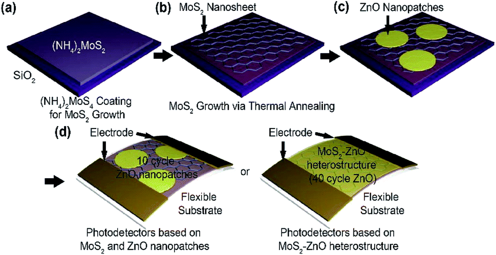 | ||
| Fig. 1 Schematic diagram of the MoS2 nanosheets with ZnO nanopatches synthesis. (a) Spin-coating of (NH4)2MoS4 as a precursor for MoS2 growth on a SiO2 substrate. (b) MoS2 growth via thermal annealing. (c) Growth of ZnO nanopatches on top of MoS2 nanosheets by ALD process. (d) Fabrication of photodetectors based on MoS2–ZnO nanopatches or heterostructure. | ||
In order to observe the surface morphology of MoS2 nanosheets with ZnO nanopatches, scanning electron microscopy (SEM) was employed with regard to the process cycles of ZnO (Fig. 2(a)). MoS2 nanosheets produced by solution-based synthesis exhibited a uniform surface coverage and a continuous film on the SiO2 substrate. The surface morphologies of MoS2 nanosheets with ZnO were then investigated depending on the process cycles. At first, the partially aggregated grains and rough surface were observed, indicating that clearly displays 10-cycle ZnO nanopatches on MoS2 nanosheets over the entire area (Fig. 2(a)(ii)). Formation of granular surface is common for epitaxial ZnO films produced by the ALD process.17,18 When increasing the ZnO film thickness by the process cycles, ZnO nanopatches with island-shape disappear, and flat thin films were formed in the MoS2 nanosheets (Fig. S1†). Moreover, atomic force microscopy (AFM) analysis was carried out to confirm the surface roughness of MoS2 nanosheets with ZnO nanopatches (Fig. 2(b)). These results were similar to surface morphologies identified by SEM analysis. Interestingly, surface roughness of MoS2 nanosheets with ZnO nanopatches at 10 cycles was the highest (∼0.57 nm) due to the presence of numerous ZnO grains at the initial deposition stage (Fig. 2(c)). When the process cycles for ZnO growth were increased, the RMS roughness decreased. This phenomenon could be understood by the formation of ZnO film at the increased process cycles. In order to provide the exact height profiles of as-deposited ZnO, XRR (X-ray specular reflectivity) was employed to confirm the thickness of thin film more accurately (Fig. S2†). In the case of 10 cycles-ZnO, the thickness cannot be measured because the thin film was not formed. This result indirectly predicts that 10 cycles-ZnO is formed with nanopatches. Furthermore, we could identify that the thickness becomes increases gradually from several nm to ∼10 nm with increasing the number of cycles and then the ZnO thin film is formed eventually. Fig. 2(d) is a photograph of the large area-based MoS2 nanosheets with ZnO on an 8 inch SiO2 substrate. Notably, the hybrid film fabricated using this approach was uniform over the whole area. Furthermore, MoS2 nanosheets with ZnO were successfully transferred onto the quartz substrate (2 cm × 2 cm) in order to confirm the applicability to the transparent electronic devices (Fig. 2(e)). Optical transmittance characterization was carried out using UV-vis spectroscopy (Fig. 2(f)). Herein, there was a difference in the optical transmittance with and without MoS2. In general, the absorption spectra of ZnO nanoparticles depend on the method of fabrication, shape, and particle size. In this study, the optical transmittance spectra based on ZnO–MoS2 hybrid films showed absorption peaks at 335 nm and 345 nm, and the two absorption peaks gradually increased as the number of ZnO cycles increased. The decrease in transmittance was related to an increase in the thickness of the films and it reveals a relatively low thickness of the ZnO films. Since the relatively thin ZnO was formed using the ALD process and act as a nanopatch, it only contributes to the healing of numerous defect sites, such as imperfections and impurities, in as-synthesized MoS2 film.
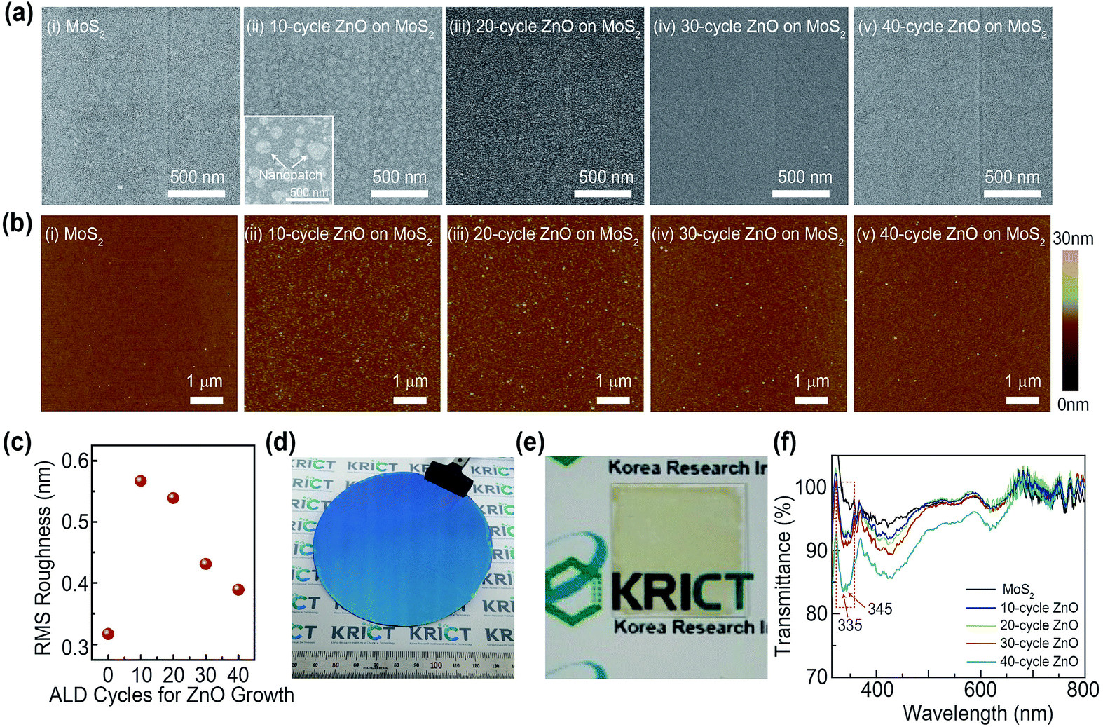 | ||
| Fig. 2 (a) Scanning electron microscopy (SEM) and (b) atomic force microscopy (AFM) images, and (c) RMS roughness of MoS2 nanosheets with ZnO nanopatches as a function of the process cycles (0, 10, 20, 30, and 40 cycles) during ALD process. Picture of large-area MoS2 and ZnO hybrid film on the 8 inch SiO2 substrate (d) and the transferred MoS2 nanosheets with ZnO nanopatches (40 cycles) (e). (f) Optical transmittance of ZnO–MoS2 hybrid film on a PET (polyethylene terephthalate) substrate for diverse ALD cycles (0, 10, 20, 30, and 40 cycles). | ||
In order to clarify the characteristics of chemical bonding in the MoS2 nanosheets with ZnO nanopatch, Raman spectroscopy is employed. There are two representative Raman modes in MoS2.19 The A1g mode is originated from the out-of-plane vibrations of molybdenum atoms, and the E12g mode is responsible for the in-plane vibrations of molybdenum and sulfur atoms. Remarkably, the Raman shift was almost constant regardless of the process cycle of ZnO film (Fig. 3(a)). Furthermore, the frequency difference of A1g mode and E12g dmode was approximately 21.6 cm−1 for the entire process condition (Fig. 3(b)). These results indicate that the structure of as-synthesized MoS2 nanosheets were well-maintained without any structural deformation during the deposition process of ZnO film. X-ray photoelectron spectroscopy (XPS) was also carried out to examine the chemical composition of the MoS2 nanosheets with ZnO nanopatch (Fig. 3(c)). Herein, the Mo 3d, S 2p core level spectra for the MoS2 nanosheets and the Zn 2p, O 1 s core level spectra related to the deposited ZnO were explored for the structural analysis of the MoS2–ZnO hybrid film. For the pristine MoS2 nanosheets, the Mo 3d3/2 and 3d5/2 peaks were located at binding energy (EB) of 232.5 eV and 229.3 eV, respectively. S 2p1/2 and 2p3/2 peaks at EB of 163.3 eV and 162 eV, respectively, were obtained in pristine MoS2 nanosheets, revealing that MoS2 was synthesized successfully using the solution process.14 Furthermore, the intensity of Mo 3d and S 2p core level spectra decreased as the process cycle of ZnO increased. In the Zn 2p core level spectra, Zn 2p1/2 at the higher binding energy and Zn 2p3/2 at the lower binding energy was observed. The difference in binding energy between the Zn 2p3/2 and Zn 2p1/2 was about 23 eV. This value, originated from the spin–orbit splitting of energy level, is consistent with previous reports that demonstrated the existence of ZnO.20 Moreover, the intensity of Zn 2p core level spectra increased as the deposition cycle of ZnO film increased. Typically, XPS is known as a powerful surface analysis tool with surface-sensitive technique. As increasing the number of ZnO cycles, the coverage region of ZnO on the MoS2 surface is increased. So, when the incident X-ray beam is injected on the MoS2–ZnO hybrid structures, the peak intensity and composition ratio could be altered. In other words, the Mo 3d and S 2p peaks become decreased as increasing the number of ZnO cycles. Whereas, the Zn 2p peaks related to ZnO become increased. Atomic concentration of MoS2–ZnO hybrid structure as a function of the number of ZnO cycles was represented in the Fig. S3.† In the O 1s core level spectra, O 1s core level spectrum was located at EB of 529.9 eV, indicating the presence of oxygen atoms in the crystal lattice without any oxygen vacancies. With increasing process cycles of ZnO film, the prominent extra peaks at EB of 531.6 eV increased. This phenomenon indicates the formation of oxygen atoms in the ZnO lattice with oxygen vacancies.
 | ||
| Fig. 3 (a) Raman spectra and (b) frequency difference between A1g mode and E12g mode of MoS2 nanosheets with ZnO nanopatches (process cycle: 10, 20, 30, and 40 cycles). (c) X-ray photoelectron spectroscopy (XPS) of MoS2 nanosheets with ZnO nanopatches. (i) Mo 3d, (ii) S 2p, (iii) Zn 2p, and (iv) O 1s core level spectra of MoS2 nanosheets with ZnO nanopatches. | ||
Fig. 4 (a–i) is an optical image of an electronic device based on a MoS2 nanosheet with a ZnO nanopatch. Here, the width and length of the channel were 40 μm, 200 μm, respectively. In order to clarify the electrical properties, output curves were examined depending on the number of ZnO cycles. Thereby, we could confirm the improved electrical properties with increasing the number of ZnO (Fig. S4†). This behavior could be understood by the fact that as-deposited ZnO contribute to heal the numerous defect sites in MoS2. Furthermore, transfer characteristics with back gate configuration were investigated for MoS2 nanosheets with a ZnO nanopatch (process cycle: 10, 20, 30, 40 cycles) under cyclic UV light irradiation (λ = 254 nm) (Fig. 4(a)(ii–vi)). Pristine MoS2 shows p-type characteristics due to the adsorbed oxygen atoms on the thin MoS2 surface in an arbitrary environment. With increasing the process cycles of ZnO films, a lot of photo-excited electrons were transferred to the ZnO film with a higher work-function than MoS2.21 Thus, the threshold voltage of MoS2 nanosheets was shifted to a more positive voltage, and their photocurrent significantly improved due to the high sensitivity of the ZnO film under UV exposure. The dependence of the photocurrent response in the UV region on the process cycle of ZnO at bias voltage of 10 V (Fig. 4(b)) was investigated. The photocurrent increased considerably with increasing process cycles. MoS2 nanosheets with 40 cycle-ZnO experienced the highest photocurrent owing to the unique properties of ZnO.22 The rise and decay time for photodetectors based on MoS2–ZnO heterostructure was calculated in Table S1.† With increasing the number of ZnO cycles, the deep level defect states (DLDS) originated form the sulfur vacancies in MoS2 crystal become disappeared and the recombination rate of photo-excited electron–hole pairs was decreased also. Our photodetectors based on MoS2–ZnO hybrid structures could improve the photoresponsivity as well as heal the several defect sites in MoS2 crystals by introducing ZnO. The relevant working principle of photodetector based on MoS2–ZnO hybrid film was depicted in Fig. S5.† The photocurrent response of MoS2 nanosheets with 40 cycle-ZnO was identified depending on the bias voltage (Fig. 4(c)). At increasing bias voltage, the photocurrent response of the MoS2–ZnO hybrid film increased dramatically and the highest photoresponsivity was estimated to 2.7 A/W at a bias voltage of 40 V. Table S2 in ESI† exhibits the parameters of MoS2 based ultraviolet photodetectors, indicating that performance for our photodetectors based on ZnO–MoS2 hybrid film is more competitive than previous reports. Furthermore, the variation of photocurrent was evaluated to confirm the applicability to flexible optoelectronic devices based on MoS2 nanosheets with ZnO nanopatch (Fig. 4(d)). PMMA-assisted wet transfer method was employed to transfer as-fabricated film to the flexible PET substrates. Fig. 4(d) shows the bending process of the MoS2–ZnO hybrid film. The variations of the photocurrent response of pristine MoS2 and MoS2–ZnO film (bending radius = 3 mm) as a function of the number of bending cycles (up to 10![[thin space (1/6-em)]](https://www.rsc.org/images/entities/char_2009.gif) 000 cycles) were examined. Remarkably, pristine MoS2 and MoS2–ZnO film do not exhibit dramatic changes upon increase of bending cycles. This reveals that the deposited ZnO film is relatively thin. When only ZnO exists, the variation of electrical properties were less than 3% after the bending process (Fig. S6†). Therefore, it does not influence the large structural deformation under the mechanical stress. We believe that the TMDs-based hybrid film in this study will be a promising candidate for applications requiring high efficient and flexible opto-electrical properties.
000 cycles) were examined. Remarkably, pristine MoS2 and MoS2–ZnO film do not exhibit dramatic changes upon increase of bending cycles. This reveals that the deposited ZnO film is relatively thin. When only ZnO exists, the variation of electrical properties were less than 3% after the bending process (Fig. S6†). Therefore, it does not influence the large structural deformation under the mechanical stress. We believe that the TMDs-based hybrid film in this study will be a promising candidate for applications requiring high efficient and flexible opto-electrical properties.
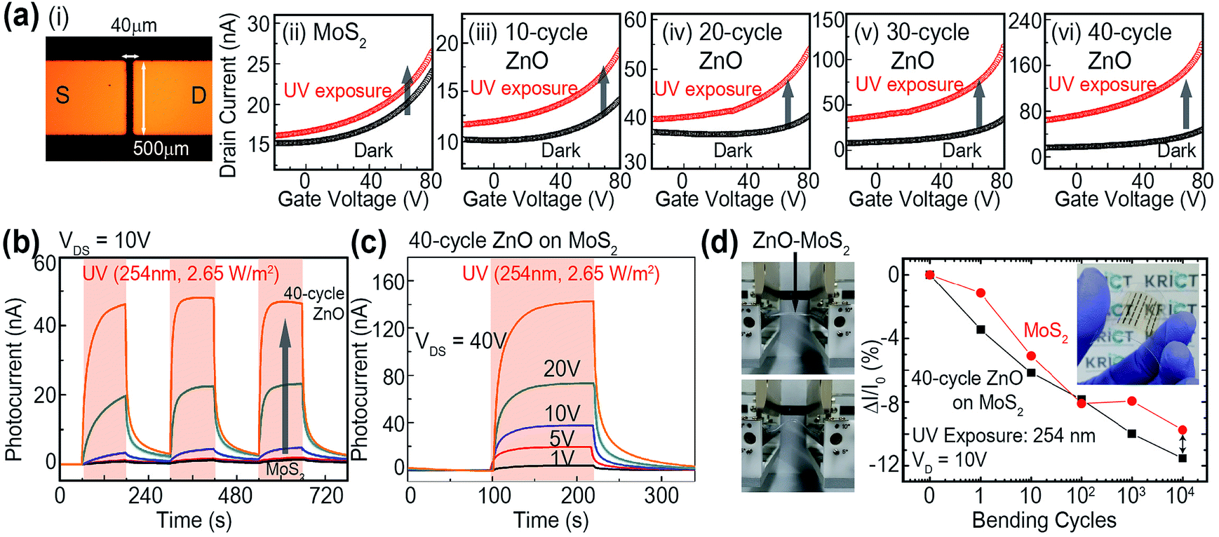 | ||
| Fig. 4 (a-i) Optical image of an electronic device based on MoS2 nanosheets with ZnO nanopatches. (a-ii)–(a-vi) Transfer curve of MoS2 nanosheets with ZnO nanopatches. (b) Time-dependent photocurrent of MoS2 nanosheets with ZnO nanopatches (process cycle: 10, 20, 30, and 40 cycle) under cyclic UV light irradiation at a bias voltage (VDS) = 10 V. (c) Time-dependent photocurrent of MoS2 nanosheets with ZnO nanopatches as a function of the bias voltage. (d) Picture of bending test using ZnO–MoS2 hybrid film on a PET substrate and variation of photocurrent as a function of bending cycles (bending radius = 3 mm). | ||
Conclusions
We demonstrated the fabrication of flexible photodetectors based on MoS2 nanosheets and ZnO nanopatches. ZnO with high efficient photocurrent heals the numerous defect sites, such as imperfections and impurities. Therefore, the carrier transport properties of hybrid films could be improved by deposition of ZnO films, and the photocurrent can bes significantly increased by reducing the photo-excited electron–hole recombination rate. The MoS2–ZnO hybrid film for the bending test was transferred onto the flexible PET substrate using a PMMA-assisted wet transfer method. It was found that the degradation of the photocurrent induced by the bending process was not changed dramatically due to the thin thickness of ZnO nanopatches. Our MoS2–ZnO hybrid film based photodetectors are expected to provide a new approach for future applications of outstanding electronic devices with high efficiency and flexibility.Conflicts of interest
There are no conflicts to declare.Acknowledgements
This research was supported by a grant (2011-0031636) from the Center for Advanced Soft Electronics under the Global Frontier Research Program of the Ministry of Science, ICT and Future Planning, Korea. This research was also supported by Multi-Ministry Collaborative R&D Program (Development of Techniques for Identification and Analysis of Gas Molecules to Protect Against Toxic Substances) through the National Research Foundation of Korea (NRF) funded by KNPA, MSIT, MOTIE, ME, and NFA (NRF-2017M3D9A1073502).Notes and references
- H. Wang, H. Yuan, S. S. Hong, Y. Li and Y. Cui, Chem. Soc. Rev., 2015, 44, 2664–2680 RSC.
- R. Lv, J. A. Robinson, R. E. Schaak, D. Sun, Y. Sun, T. E. Mallouk and M. Terrones, Acc. Chem. Res., 2015, 48, 56–64 CrossRef CAS PubMed.
- J. Zhu, J. Wu, Y. Sun, J. Hunag, Y. Xia, H. Wang, H. Wang, Y. Wang, Q. Yi and G. Zou, RSC Adv., 2016, 6, 110604 RSC.
- K. F. Mak, C. Lee, J. Hone, J. Shan and T. F. Heinz, Phys. Rev. Lett., 2010, 105, 136805 CrossRef PubMed.
- H. J. Conley, B. Wang, J. I. Ziegler, R. F. Haglund, S. T. Pantelides and K. I. Bolotin, Nano Lett., 2013, 13, 3626–3630 CrossRef CAS PubMed.
- A. Molina-Sánche, K. Hummer and L. Wirtz, Surf. Sci. Rep., 2015, 70, 554–586 CrossRef.
- Z. Cheng, B. He and L. Zhou, J. Mater. Chem. A, 2015, 3, 1042 RSC.
- T. S. Sreeprasad, P. Nguyen, N. Kim and V. Berry, Nano Lett., 2013, 13, 4434–4444 CrossRef CAS PubMed.
- Y. Shi, J.-K. Huang, L. Jin, Y.-T. Hsu, S. F. Yu, L. Li and H. Y. Yang, Sci. Rep., 2013, 3, 1839 CrossRef PubMed.
- D. Jariwala, S. L. Howell, K.-S. Chen, J. Kang, V. K. Sangwan, S. A. Filippone, R. Turrisi, T. J. Marks, L. J. Lauhon and M. C. Hersam, Nano Lett., 2016, 16, 497–503 CrossRef CAS PubMed.
- S. Andleeb, A. K. Singh and J. Eom, Sci. Technol. Adv. Mater., 2015, 16, 035009 CrossRef PubMed.
- M. A. Nazirzadeh, F. B. Atar, B. B. Turgut and A. K. Okyay, Sci. Rep., 2014, 4, 7103 CrossRef PubMed.
- A. Sharma, R. Kumar, B. Bhattacharyya and S. Husale, Sci. Rep., 2016, 6, 22939 CrossRef CAS.
- Y. R. Lim, W. Song, J. K. Han, Y. B. Lee, S. J. Kim, S. Myung, S. S. Lee, K.-S. An, C.-J. Choi and J. Lim, Adv. Mater., 2016, 28, 5025–5030 CrossRef CAS PubMed.
- E. Guziewicz, M. Godlewski, T. Krajewski, Ł. Wachnicki, A. Szczepanik, K. Kopalko, A. Wójcik-Głodowska, E. Przeździecka, W. Paszkowicz, E. Łusakowska, P. Kruszewski, N. Huby, G. Tallarida and S. Ferrari, J. Appl. Phys., 2009, 105, 122413 CrossRef.
- E. Janocha and C. Pettenkofer, Appl. Surf. Sci., 2011, 257, 10031–10035 CrossRef CAS.
- G. A. Velázquez-Nevárez, J. R. Vargas-García, J. Aguilar-Hernández, O. E. Vega-Becerra, F. Chen, Q. Shen and L. Zhang, Mater. Res., 2016, 19, 113–117 CrossRef.
- Z.-N. Ng, K.-Y. Chan, C.-Y. Low, S. A. Kamaruddin and M. Z. Sahdan, Ceram. Int., 2015, 41, 254–258 CrossRef.
- C. Lee, H. Yan, L. E. Brus, T. F. Heinz, J. Hone and S. Ryu, ACS Nano, 2010, 4, 2695–2700 CrossRef CAS PubMed.
- A. G. Joshi, S. Sahai, N. Gandhi, Y. G. R. Krishna and D. Haranth, Appl. Phys. Lett., 2010, 96, 123102 CrossRef.
- G. Nazir, M. F. Khan, I. Akhtar, K. Akbar, P. Gautam, H. Noh, Y. Seo, S.-H. Chun and J. Eom, RSC Adv., 2017, 7, 16890 RSC.
- K. Liu, M. Sakurai and M. Aono, Sensors, 2010, 10, 8604–8634 CrossRef CAS.
Footnote |
| † Electronic supplementary information (ESI) available. See DOI: 10.1039/c9ra00578a |
| This journal is © The Royal Society of Chemistry 2019 |