
 Open Access Article
 This Open Access Article is licensed under a Creative Commons Attribution-Non Commercial 3.0 Unported Licence
One-step hydrothermal synthesis of Ni–Fe–P/graphene nanosheet composites with excellent electromagnetic wave absorption properties
Shuo Zhao a,
Chunyu Wang*a,
Ting Sub and
Bo Zhong*a
a,
Chunyu Wang*a,
Ting Sub and
Bo Zhong*a
aSchool of Materials Science and Engineering, Harbin Institute of Technology at Weihai, Weihai 264209, People's Republic of China. E-mail: zhongbooo@126.com; wcyadam@126.com
bGreen Chemistry Centre, Collaborative Innovation Center for Light Hydrocarbon Resources, College of Chemistry and Chemical Engineering, Yantai University, Yantai, 264005, People's Republic of China
First published on 13th February 2019
Abstract
Ni–Fe–P nanoparticles/graphene nanosheet (Ni–Fe–P/GNs) composites were successfully synthesized by a simple one-step hydrothermal method. Specifically, Ni2+ and Fe2+ were reduced by using milder sodium hypophosphite as a reducing agent in aqueous solution. SEM and TEM images show that a large number of Ni–Fe–P nanoscale microspheres are uniformly deposited on graphene nanosheets (GNs). At the thickness of 3.9 mm, the minimum reflection loss (RL) of Ni–Fe–P/GNs reaches −50.5 dB at 5.3 GHz. In addition, Ni–Fe–P/GNs exhibit a maximum absorption bandwidth of 5.0 GHz (13.0–18.0 GHz) at the thickness of 1.6 mm. The significant electromagnetic absorption characteristics of the Ni–Fe–P/GN composites can be attributed to the addition of magnetic particles to tune the dielectric properties of graphene to achieve good impedance matching. Therefore, Ni–Fe–P/GN is expected to be an attractive candidate for an electromagnetic wave absorber.
1. Introduction
Electronic communication equipment has been widely used in human society, but the electromagnetic (EM) waves on which it lives have caused a lot of pollution at the same time.1,2 Studies have shown that electromagnetic waves can cause harm to human neurological, immune, and reproductive systems as well as cause cancer.3–5 Therefore, it is necessary to develop a high performance EM absorbent.Conventional EM wave absorbing materials mainly include ferrite, magnetic metal and carbon materials like graphite. Among them, carbon-based composite materials based on carbon materials are excellent in the field of EM wave absorption, and have the advantages of good electrical conductivity, light weight and good chemical stability.6–9 Graphene, which is a carbon-based material, may become a new type of composite EM wave absorbing material due to its special surface characteristics and layered structure.10,11 However, the high permittivity of graphene may lead to impedance mismatch, which in turn affects the EM wave absorption properties of the composite.12,13 It is well known that the EM impedance matching of the absorber is the main factors determining the EM wave absorption characteristics. According to the principle of impedance matching, the combination of magnetic loss and dielectric loss materials is considered to be an effective method to achieve impedance matching of high performance EM absorbing materials. Studies have shown that graphene can be used as a substrate in combination with Fe3O4, CuS, SiC, TiO2, etc., and have good EM wave absorption characteristics.14–17 In addition, magnetic nanoparticles (Fe, Co, Ni) can also be combined with graphene to form composite materials, and have a significant effect in the field of EM wave absorption.18–22 Among them, the research on Ni is the most. Chen et al.,23 grew a hexagonal close-packed Ni nanocrystal on the surface of graphene by a one-step solution phase method, and a minimum reflection loss (RL) of −17.8 dB occurred when the sample thickness was 5 mm. Fang et al.,24 used electrochemical deposition to deposit Ni on the graphene nanosheets. When the sample thickness is 1.5 mm, it corresponds to a minimum RL value of 16.0 dB at 9.15 GHz. Li et al.,25 used a one-pot method to prepare a sandwich-structured composite which Ni particles are in the middle and grapheme sheets and C are on both sides, showing a minimum RL value of −34.2 dB at a thickness of 1.6 mm and a frequency of 13.9 GHz. It can be seen that most of the composite materials in which Ni and graphene are combined have less strength in EM wave absorption. Combining other absorbers on the basis of Ni/graphene to form a multi-component composite is an effective method for improving the EM wave absorption characteristics. The introduction of Fe, which is also a magnetic metal, into Ni/graphene as an EM wave absorber is relatively rare. Moreover, in the related research, Fe is mainly added to Ni/graphene in the form of a substance in a multi-step preparation process to form a multi-component composite.26,27
In this paper, a milder sodium hypophosphite was used as a reducing agent to form Ni–Fe–P/GNs (Ni–Fe–P alloy/graphene nanosheets) nanocomposite by in situ formation of Ni and Fe alloys on graphene nanosheets by one-step hydrothermal method. Ni–Fe–P/GNs were characterized by different analytical methods, and its EM wave absorption characteristics were detected and analyzed. In addition, Ni–P/GNs (Ni–P alloy/graphene nanosheets) was synthesized by the same method, and compared with Ni–Fe–P/GNs to investigate the effects of the introduction of Fe on the microstructure and EM wave absorption characteristics of Ni–P/GNs.
2. Experimental
2.1. Materials
Nickel sulfate hexahydrate (NiSO4·6H2O), ferrous sulfate heptahydrate (FeSO4·7H2O), sodium citrate (Na3C6H5O7·2H2O), anhydrous sodium acetate (CH3COONa), boric acid (H3BO3), sodium hypophosphite (NaH2PO2·H2O). Graphene nanosheets are manufactured by ourselves through physical methods. The specific method is that we use expanded graphite as a raw material to cause supersonic collision with the high pressure gas produced by a fluidized bed to obtain graphene nanosheets. All chemicals were of analytical grade and could be used without further purification.2.2. Synthesis of Ni–P/GNs
The composite of phosphorus-containing nickel microsphere composite graphene nanosheets (GNs) was synthesized by a simple hydrothermal method. GNs (5 g) were first suspended in 200 mL of 65% concentrated nitric acid and the mixture was magnetically stirred for 18 hours. Then 0.25 g of acidified GNs, 3 g NiSO4·7H2O, 6 g Na3C6H5O7·2H2O, 3 g NaH2PO2·H2O and 2 g CH3COONa were dissolved in 30 mL of deionized water. The mixture was underwent 40 minutes of ultrasonic oscillation. Subsequently, the mixture was transferred into a Teflon-lined stainless-steel autoclave of 150 °C for 2 hours. After the reaction was completed, the product was naturally cooled to room temperature. The product was then washed with deionizer water several times and separated using the suction filter. The resulting product was vacuum dried at 50 °C for 6 h and labeled as Ni–P/GNs.2.3. Synthesis of Ni–Fe–P/GNs
The introduction of Fe is based on the synthesis of Ni–P/GNs. The pretreatment of GNs was the same as that of Ni–P/GNs. 1.5 g FeSO4·7H2O g, 1.5 g NiSO4·7H2O, 6 g Na3C6H5O7·2H2O, 3 g NaH2PO2·H2O and 2 g H3BO3 were added in 30 mL of deionized water. 0.25 g of acidified GNs and the prepared reaction solution were dispersed under ultrasonic vibration for 40 minutes. The mixture was then transferred to a Teflon-lined stainless steel autoclave at 150 °C for 2 hours. After the reaction was completed, it was naturally cooled to room temperature. The product was washed several times with deionized water and separated using the suction filter. The resulting product was dried under vacuum at 50 °C for 6 hours and was labeled as Ni–Fe–P/GNs.2.4. Characterization
The morphology and microstructure of the samples were characterized by field-emission scanning electron microscopy (SEM, MERLIN Compact, Zeiss) and transmission electron microscopy (TEM, JEOL JEM-2010). Raman spectra were recorded on (RENISHAW inVia Raman microscope) spectrometer with 532 nm laser. The crystalline structures were characterized by (DX-2700, Dandong Haoyuan Co. China) X-ray diffractometer with Cu Kα radiation.2.5. Measurements of EM absorption properties
In order to evaluate the EM wave absorption properties of Ni–Fe–P/GNs and compare them with Ni–P/GNs and GNs, the composite samples were prepared by mixing the sample powder and paraffin in a mass ratio of 2![[thin space (1/6-em)]](https://www.rsc.org/images/entities/char_2009.gif) :8. The mixtures were then pressed into a ring having an inner diameter of 3.04 mm, an outer diameter of 7 mm, and a thickness of 3 mm. The electromagnetic parameters of the composite were measured on a vector network analyzer (VNA; Agilent N5245A) in a transmission/reflection mode of 2–18 GHz.
:8. The mixtures were then pressed into a ring having an inner diameter of 3.04 mm, an outer diameter of 7 mm, and a thickness of 3 mm. The electromagnetic parameters of the composite were measured on a vector network analyzer (VNA; Agilent N5245A) in a transmission/reflection mode of 2–18 GHz.
3. Results and discussion
3.1. Formation and morphology analysis
Fig. 1(a)–(h) and 2(a) and (c) are SEM and TEM images respectively, showing the microstructures of Ni–P/GNs and Ni–Fe–P/GNs. As shown in Fig. 1(a)–(c), it is apparent that a large amount of Ni–P microspheres are distributed almost uniformly on the surface of the GNs, except that a small amount of particles tend to aggregate. In combination with Fig. 2(a), the Ni–P microspheres have a diameter between 200 nm and 500 nm, and the adhesion of the foreign particles causes the SAED of Ni–P/GNs to exhibit a polycrystalline ring shape. The Ni–P microspheres on the surface of the graphene function to prevent re-stacking of the graphene nanosheets and are encapsulated by the sandwich graphene nanosheets. Further, Fig. 1(c) shows that a part of the graphene nanosheet is translucent, and it is possible to obscurely see that a part of the Ni–P microspheres are uniformly distributed on the other side.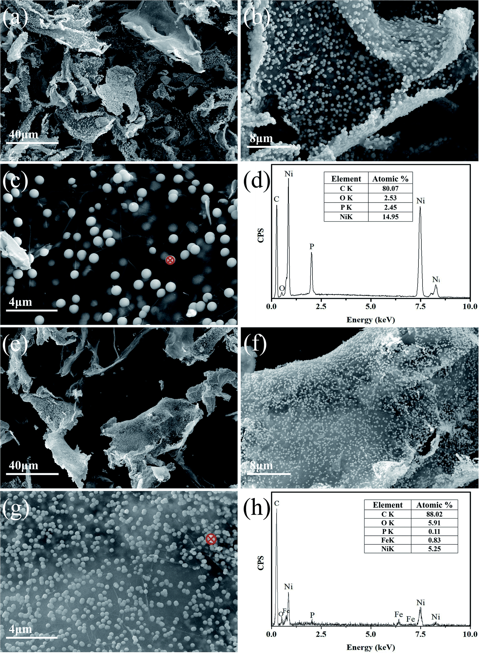 | ||
| Fig. 1 SEM images and EDS spectrum of Ni–P/GNs and Ni–Fe–P/GNs: (a and b) low magnification SEM images of Ni–P/GNs, (c) high magnification SEM images of Ni–P/GNs, (d) EDS spectrum is collected from the red mark part in (c), (e and f) low magnification SEM images of Ni–Fe–P/GNs, (g) high magnification SEM images of Ni–Fe–P/GNs and (h) EDS spectrum is collected from the red mark part in (g). | ||
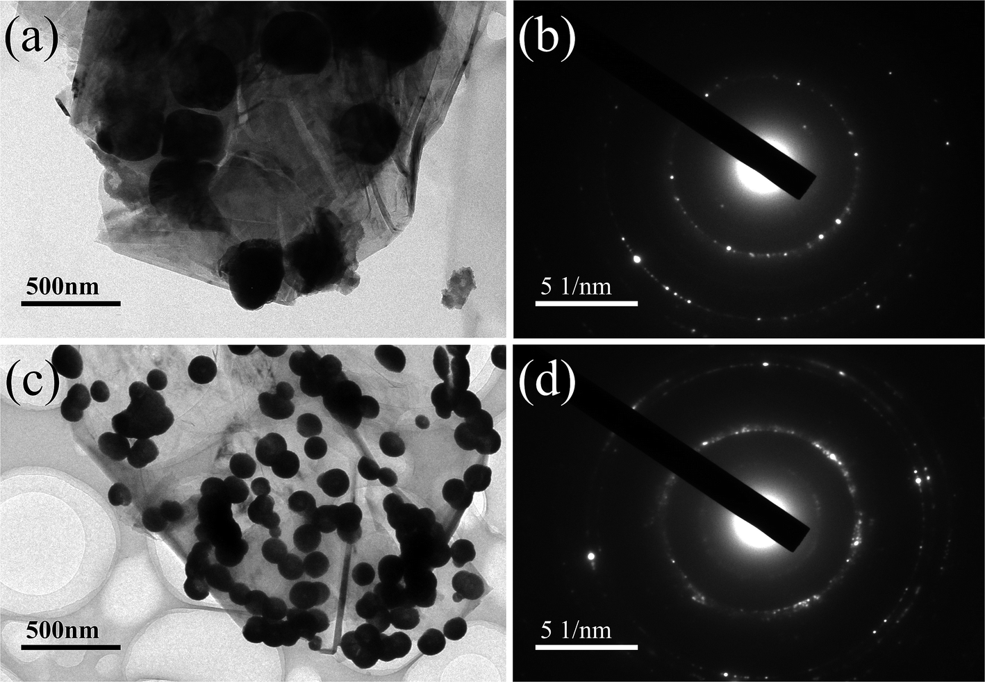 | ||
| Fig. 2 (a) TEM images of Ni–P/GNs, (b) SAED pattern of Ni–P/GNs, (c) TEM images of Ni–Fe–P/GNs, and (d) SAED pattern of Ni–Fe–P/GNs. | ||
The SEM microscopic morphology of Ni–Fe–P/GNs is shown in Fig. 1(e)–(g). It can be seen that Ni–Fe–P are distributed in the form of microspheres on the surface of graphene like Ni–P. Referring to Fig. 2(c), the particle size of the Ni–Fe–P microspheres is between 50 nm and 200 nm, and the degree of aggregation of the particles is higher than that of Ni–P. Moreover, at the same reaction temperature and reaction time, the particle diameter of the Ni–Fe–P particles is smaller than the particle diameter of the Ni particles. This is because the introduction of Fe reduces the nucleation rate and growth rate, resulting in smaller particle sizes and more sparse distribution than Ni particles. And Fe is more likely to agglomerate relative to nickel during the growth process, which will cause the nickel–iron alloy to also agglomerate together.
Through SEM analysis of the sample, we can find that using graphene nanosheets to support Ni and Ni–Fe takes only 2 hours to obtain a uniformly distributed nanoparticle product. This is much faster than the traditional use of graphene oxide to load magnetic metals.28,29
The elemental composition of each sample was determined by EDS measurement. Fig. 1(d) and (h) show the elemental distributions of the detected Ni–P/GNs and Ni–Fe–P/GNs. The atomic ratio of Ni to P in Ni–P/GNs is about 6:1, and the atomic ratio of Ni to Fe and Ni to P in Ni–Fe–P/GNs are about 6:1 and 47:1, respectively. It can be seen from EDS that Fe is successfully introduced into Ni–P microspheres, but the Fe content is relatively lower than Ni, which also shows that the growth of Fe on graphene is much more difficult than that of Ni. Carbon and oxygen should be derived from GNs. Acidification of concentrated nitric acid causes a portion of the surface of the GNs to be oxidized and produces oxygen-containing functional groups, but due to the short hydrothermal time, the residual oxygen-containing functional groups can not be completely removed. The introduction of P is derived from the use of sodium hypophosphite as a reducing agent to form a nickel–phosphorus alloy with Ni. The atomic ratio of Ni to P in Ni–Fe–P/GNs is less than that of Ni–P/GNs, because most Ni in Ni–Fe–P/GNs preferentially combine with Fe to form Ni–Fe alloy, while the remaining Ni has the opportunity to form Ni–P alloy with P. The difference in peak intensity between C and O reflects that the content of C is higher than O, indicating that the acidification of concentrated nitric acid causes a small portion of the surface of GNs to be oxidized, and the surface of graphene is relatively intact with relatively few defects. This will be further confirmed by Raman spectroscopy.
3.2. Structural characterization
The crystal structure and texture of the sample were characterized by XRD. As shown in Fig. 3(a), it can be seen that the diffraction peaks at 26.488°, 54.644° and 77.344° can be directed to the two-dimensional planar structure of the graphene nanosheets and are well attributed to the crystal faces of (002), (004) and (110). The peak at 2θ = 26.488° is the conventional stacking peak of graphite, which indicates that the graphene nanosheets used in this experiment are stacked from a certain amount of graphene and have a certain thickness.30 From the Ni–P/GNs curve in Fig. 3(a), we found that the dispersion peak between 2θ = 40–50° corresponds to the Ni–P alloy. Due to the addition of the phosphorus, the XRD curve forms a typical bread-like curve at 2θ = 40° to 50° due to the poorly crystalline Ni–P alloy.31,32 The peak at about 44° corresponds to the (111) plane of the pure nickel phase (PDF 87-0712), so pure nickel may also be present in the system. In the Ni–Fe–P/GNs curve, the characteristic diffraction peaks at about 44.5° correspond to the (111) crystal planes in the face-centered cubic crystal structure of the Ni–Fe alloy (PDF 88-1715). The dispersion peak similar to Ni–P/GNs appearing in the range of 2θ = 40–50° shows P element is also present in the Ni–Fe alloy. We can see that the peak width of the dispersion peak representing Ni–P becomes narrowed after the introduction of Fe, and the shape of the peak becomes more pronounced, which also indicates that the crystallinity of the Ni–Fe–P alloy is better than that of Ni–P. The small diffraction peak at about 36.5° corresponds to the (031) crystal plane of Ni3P (PDF 34-0501), and since the crystallinity of the Ni–Fe–P alloy is preferable to Ni–P, this diffraction peak can be revealed. In order to describe the phases of Ni–P/GNs and Ni–Fe–P/GNs more clearly and intuitively, we have heat treated them. The heat treatment temperature was set to 500 °C and 700 °C, the heating rate was 5 °C min−1, and this temperature was maintained for 1 h. As shown in Fig. 3(b) and (c), the Ni–P/GNs and Ni–Fe–P/GNs after heat treatment showed better crystallinity than those without heat treatment, and the internal diffraction peaks appeared. Ni–P/GNs at 500 °C and 700 °C showed obvious diffraction peaks, but Ni–Fe–P/GNs showed obvious diffraction peaks at 700 °C, while peaks at 500 °C appeared still looks blurry. As can be seen from the Fig. 3(b), Ni (PDF 87-0712) and Ni3P (PDF 74-1384) are mainly present in Ni–P/GNs. The diffraction peaks at about 47.3° and 48.1° are attributable to the (301) and (213) crystal faces of Ni5P4 (PDF 89-2588). Fig. 3(c) shows that Ni–Fe–P/GNs mainly contain Ni3Fe (PDF 88-1715), Ni (PDF 87-0712) and Ni3P (PDF 74-1384). The diffraction peaks of Ni3Fe and Ni coincide at about 44.3°, 51.6° and 76.1°, and correspond to their (111), (200) and (220) crystal faces. Comparing the three curves representing GNs, Ni–P/GNs and Ni–Fe–P/GNs, we found the intensity of the diffraction peak at 2θ = 26.488° corresponding to the graphene nanosheets in Ni–P/GNs and Ni–Fe–P/GN are weaker than the curve of GNs. The strong peak at 2θ = 26.488° corresponds to the (002) crystal plane of graphite, and its peak shape is regular and the peak width is narrow, indicating a good graphite structure. This is due to the use of graphene microchips, which have not undergone a common redox step, so graphene is in an ordered stacked state.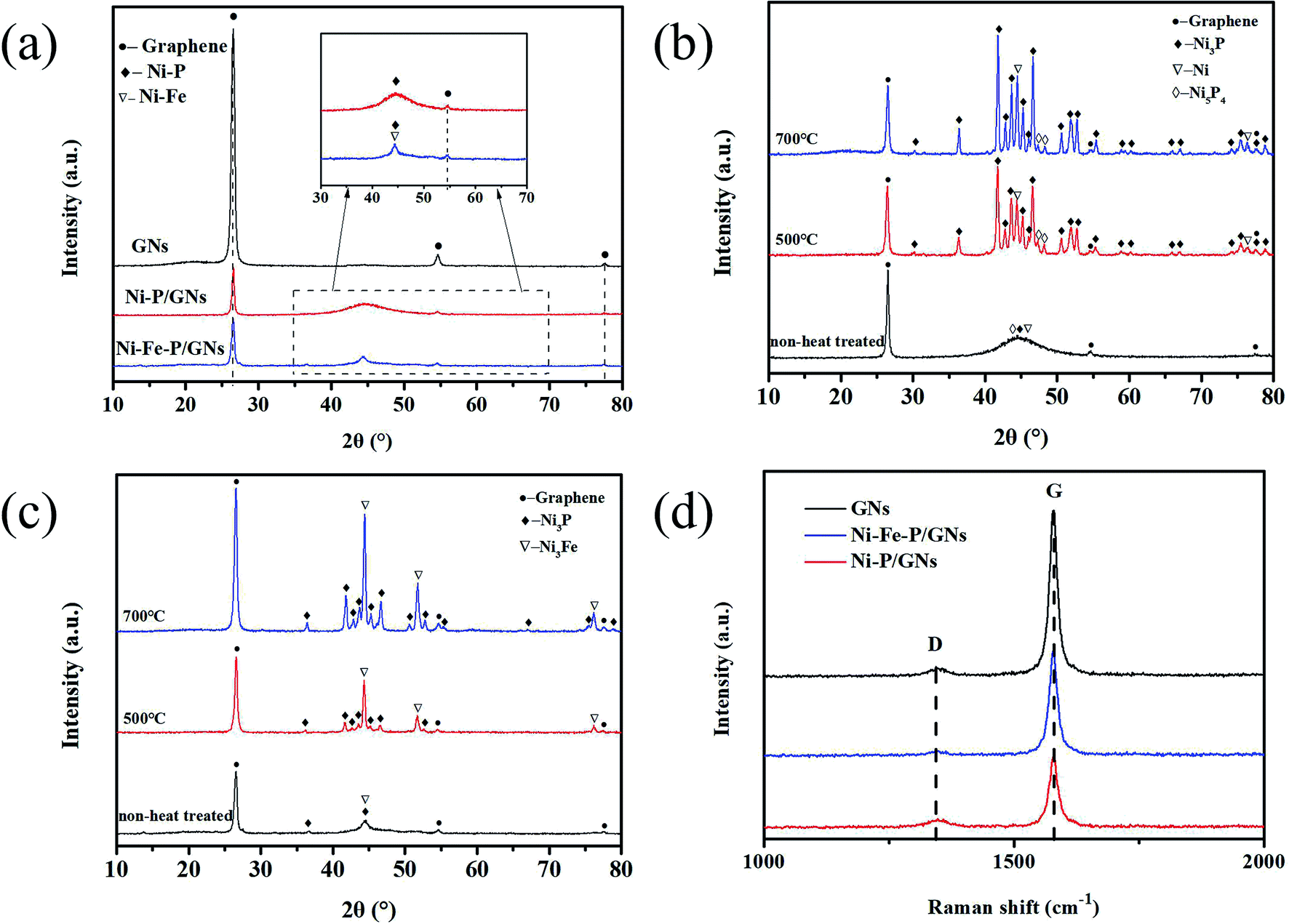 | ||
| Fig. 3 XRD patterns of (a) GNs, Ni–P/GNs and Ni–Fe–P/GNs without heat treatment, (b) Ni–P/GNs with heat treatment, (c) Ni–Fe–P/GNs with heat treatment and (d) Raman spectra of the GNs, Ni–P/GNs and Ni–Fe–P/GNs. | ||
Raman spectroscopy is an analysis method that analyzes the scattering spectra with different frequencies of incident light to obtain molecular vibration and rotation information, and is applied to the study of molecular structure. It can be used to analyze the surface defects of graphene and the changes in the bonding state of carbon atoms. Fig. 3(d) presents the Raman spectral of graphite, GNs, Ni–P/GNs and Ni–Fe–P/GNs. There are three distinct peaks at 1350 cm−1 and 1582 cm−1, corresponding to the D-band and G-band of the carbon materials. The G-band is the main characteristic peak of the graphene material which can effectively reflect the number of graphene layers. The D-band is a disordered vibration peak of graphene that can characterize defects in graphene structures. The intensity ratio of D-band to G-band (ID/IG) can be used to indicate the defect density of grapheme.33,34 As can be seen from the figure, the ID/IG value increases significantly after the magnetic metal alloy particles are deposited on the graphene. This is because the introduction of the magnetic metal alloy particles causes an increase in the defect density of the graphene surface and forms new and smaller sp2 domains during the reduction.30,35 The ID/IG of Ni–P/GNs value is smaller than that of Ni–Fe–P/GNs because that the amount of Ni–Fe–P microspheres deposited on the GNs is not much more than that of Ni–P, and the size of the microspheres is also smaller results in a defect density on the graphene surface that is not as much as Ni–P alone. The lower G-band of Ni–P/GN and Ni–Fe–P/GNs than that of GNs is due to the in situ growth of Ni–P and Ni–Fe–P on the GNs surface, which decomposed part of the GNs layer and reduced the number of graphene layers.
3.3. EM absorption property
The EM wave absorption performance of the composite material is calculated from the combination of its complex permittivity (εr = ε′ − jε′′) and complex permeability (μr = μ′ − jμ′′).36 ε′, μ′ reflects the degree of polarization or magnetization of the material under the influence of an electric or magnetic field and ε′′, μ′′ reflects the measure of the loss caused by the electrical coupling torque or the magnetic coupling torque rearrangement of the material under an electric or magnetic field. In this experiment, GNs/Ni–P/GNs and Ni–Fe–P/GNs were mixed with paraffin at the same mass fraction of 20 wt%, respectively. Their complex permittivity and complex permeability in the range of 2–18 GHz were measured by the vector network analyzer. Fig. 4(a) shows the variation of the electromagnetic parameters of GNs, Ni–P/GNs and Ni–Fe–P/GNs at 2–18 GHz. We can observe that the ε′ of GNs, Ni–P/GNs and Ni–Fe–P/GNs all show a general decreasing trend at 2–18 GHz with a tiny fluctuation. This is due to the fact that changes in the electric field at high frequencies increase the hysteresis of the dipole polarization response.27 As shown in Fig. 4(b), it can be seen that the ε′′ values of Ni–P/GNs varied from 0.94 to 6.94 with a strong peak at 2–18 GHz which is due to the increase of the bound charge in the material, and the increased bound charge produces a high displacement current in the material.37 While the ε′′ values of Ni–Fe–P/GNs fluctuates between 4.2 and 6.1, which are both lower than that of GNs with Ni–P/GNs at 2–18 GHz. The complex permittivity is mainly affected by the conductivity and polarizations.38 The complex permittivity of Ni–P/GNs and Ni–Fe–P/GNs have fluctuations attributable to the interfacial polarization caused by the multilayer interface between the foreign magnetic particles and the graphene microchip and the dipolar polarization generated by the surface defects of the grapheme.35 That ε′ and ε′′ of Ni–P/GNs and Ni–Fe–P/GNs are lower than that of GNs is due to the fact that the particles disperse the graphene sheets, which destroys part of the graphene conductive network and the isolation effect of the particles, resulting in a decrease in the conductivity of the composite material.39 Fig. 4(c) shows the real and imaginary parts of the complex permeability of the three materials. The μ′ of Ni–P/GNs and Ni–Fe–P/GNs varying from 0.86 to 1.35 and 0.93 to 1.27 presented a slow decline at 2.0–10.0 GHz and a relatively large increase in 10.0–18.0 GHz, in which Ni–P/GNs had a large fluctuation. GNs showed the opposite trend from Ni–P/GNs and Ni–Fe–P/GNs, which increased at 2.0–13.0 GHz and decreased at 13.0–18.0 GHz, varying from 0.96 to 1.07. As shown in Fig. 4(d), at 2.0–6.3 GHz, the μ′′ of Ni–Fe–P/GNs is larger than those of Ni–P/GNs and GNs, and at 13.9–18.0 GHz, the μ′′ of Ni–P/GNs is the largest of the three. All three have negative values of the imaginary part of the permeability between 2–18 GHz. This is because the charge in the material moves under an applied electromagnetic field and generates a corresponding alternating electric field and an opposite magnetic field. Part of the electric field is converted into the magnetic field and radiated from the composite material in the form of magnetic energy, resulting in a negative magnetic loss.40 Generally, the magnetic loss of the absorption material comes from hysteresis loss, natural resonance, domain wall resonance exchange resonance and eddy current effects.41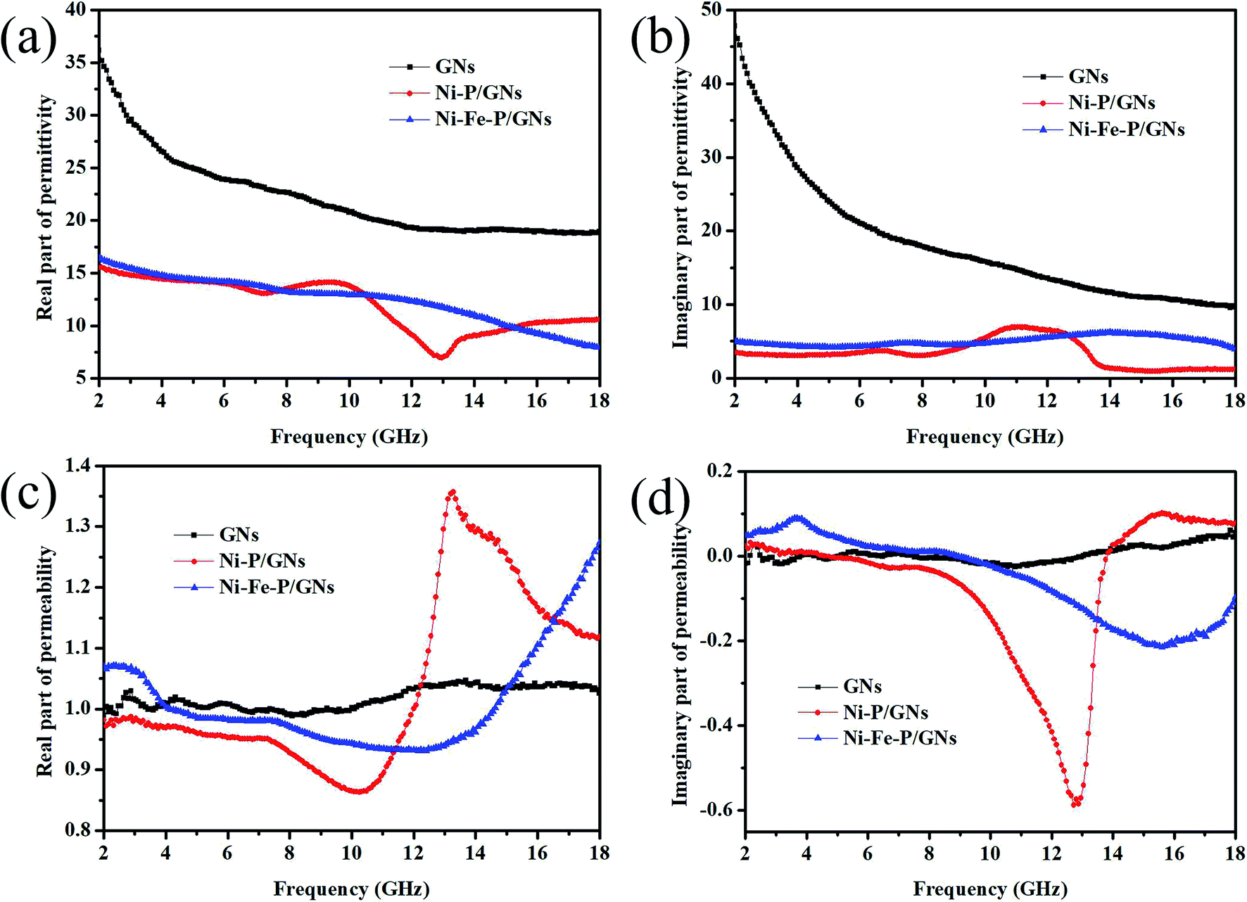 | ||
| Fig. 4 Frequency dependence of electromagnetic parameters of the samples: (a) the real part (ε′) and (b) imaginary part (ε′′) of the complex permittivity, (c) the real part (μ′) and (d) imaginary part (μ′′) of the complex permeability. | ||
Hysteresis loss usually occurs under the action of a strong magnetic field.38 The vector network analyzer tests the material in a weak electromagnetic environment, so the hysteresis loss can be eliminated in the magnetic loss mechanism; the domain wall loss occurs in the frequency range of less than 2 GHz,42 it can also be excluded; the exchange resonance is related to the size of the material. Usually when the material size reaches the micron level, its effect on magnetic loss will become minimal. The size of Ni–Fe–P/GNs is on the order of nanometers, so the exchange resonance can be eliminated.43 The eddy current loss can be verified according to the calculation: μ′′ can be expressed as the following eqn (1):44
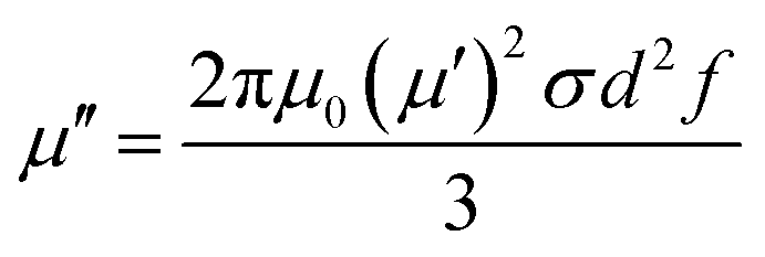 | (1) |
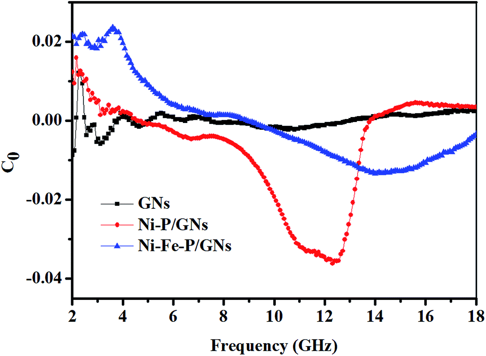 | ||
| Fig. 5 Plots of C0 versus f for GNs, Ni–P/GNs and Ni–Fe–P/GNs. | ||
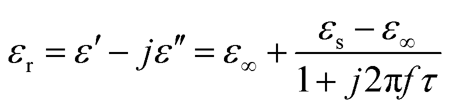
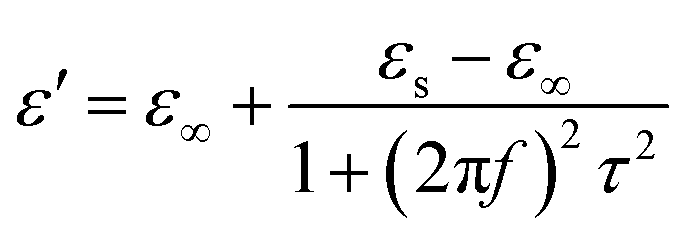
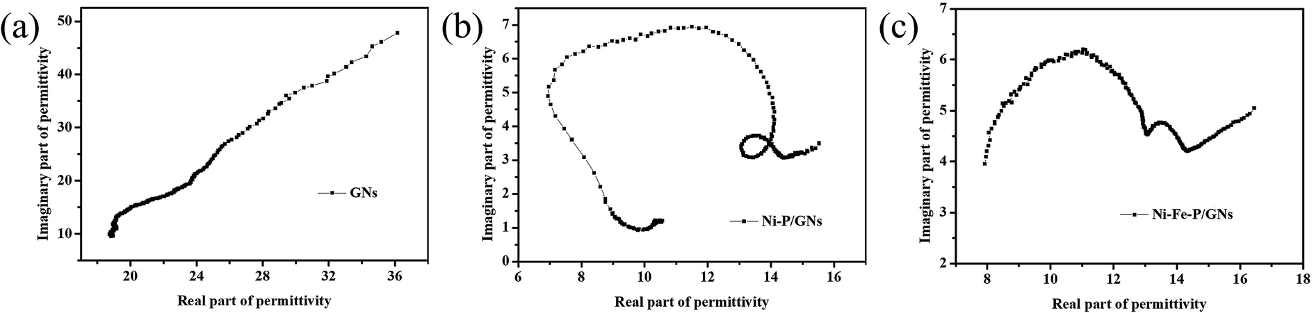
In order to explore the diversified dielectric loss mechanism in composite absorbing materials, the curves with ε′ and ε′′ as the horizontal and vertical coordinates are plotted (Fig. 6(a)–(c)). The curves are called Cole–Cole semicircle based on Debye theory.42 According to the theory of Debye dipolar relaxation, the relative complex permittivity (εr) can be expressed as follows:47–49
 | (2) |
 | (3) |
 | (4) |
 | (5) |
 | ||
| Fig. 6 Typical Cole–Cole semicircles for (a) GNs, (b) Ni–P/GNs and (c) Ni–Fe–P/GNs. | ||
In the calculation of the above equation, the shape of the curve of the obtained value may have a semicircle. This semicircle is called Cole–Cole semicircle,50,51 and each semicircle corresponds to a Debye process. As can be seen from the Fig. 6(a)–(c), there is no semicircle in the curve of GNs, which is close to a straight line. The Ni–P/GNs curve has at least three semicircles, which indicates that there are multiple dielectric relaxations in the paraffin-based Ni–P/GNs composite at 2–18 GHz. In the curve of Ni–Fe–P/GNs, there are two semicircles, and the Cole–Cole semicircle is distorted, which indicates that in addition to dielectric relaxation, there are other mechanisms in the paraffin-based Ni–Fe–P/GNs such as Maxwell–Wagner relaxation, electron polarization and dipole polarization.52 In the paraffin-based Ni–Fe–P/GNs composite absorbing material, there are multiple interfaces between Ni–Fe–P particles, GNs and paraffin. The charged multipoles at the interface interacts with external electromagnetic radiation to induce the interfacial polarization, which contributes to EM wave absorption. This interfacial polarization is caused by the migration and accumulation of charge carriers at the interface of the composites.53
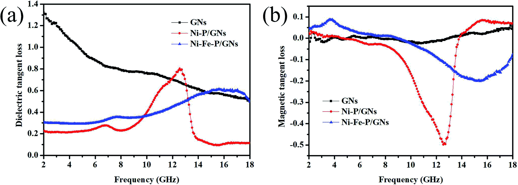
The dielectric loss tangent (tan![[thin space (1/6-em)]](https://www.rsc.org/images/entities/i_char_2009.gif) δε = ε′′/ε′) and magnetic loss tangent (tanδμ = μ′′/μ′) of GNs, Ni–P/GNs, and Ni–Fe–P/GNs shown in Fig. 7(a) and (b), which can further elucidate the EM absorption mechanism. It can be seen that the curves of tanδε and tanδμ have similar trends with the materials ε′′ and μ′′. Moreover, the tanδε and tanδμ of the three groups of samples showed a symmetric trend, and the increase of tanδε was accompanied by the decrease of tanδμ. The tanδε of GNs is obviously higher than that of Ni–P/GNs and Ni–Fe–P/GNs, while tanδμ of them is similar. This also leads to EM absorption capacity of GNs is weaker than Ni–P/GNs and Ni–Fe–P/GNs because when the tanδε and tanδμ values are close, the composite material can have better impedance matching between the dielectric loss and the magnetic loss.54 In addition, it can also be seen from Fig. 7 that the tanδε of GNs, Ni–P/GNs, and Ni–Fe–P/GNs are all significantly higher than tanδμ, which also shows that their electromagnetic wave attenuation mechanism mainly depends on the dielectric loss.
δε = ε′′/ε′) and magnetic loss tangent (tanδμ = μ′′/μ′) of GNs, Ni–P/GNs, and Ni–Fe–P/GNs shown in Fig. 7(a) and (b), which can further elucidate the EM absorption mechanism. It can be seen that the curves of tanδε and tanδμ have similar trends with the materials ε′′ and μ′′. Moreover, the tanδε and tanδμ of the three groups of samples showed a symmetric trend, and the increase of tanδε was accompanied by the decrease of tanδμ. The tanδε of GNs is obviously higher than that of Ni–P/GNs and Ni–Fe–P/GNs, while tanδμ of them is similar. This also leads to EM absorption capacity of GNs is weaker than Ni–P/GNs and Ni–Fe–P/GNs because when the tanδε and tanδμ values are close, the composite material can have better impedance matching between the dielectric loss and the magnetic loss.54 In addition, it can also be seen from Fig. 7 that the tanδε of GNs, Ni–P/GNs, and Ni–Fe–P/GNs are all significantly higher than tanδμ, which also shows that their electromagnetic wave attenuation mechanism mainly depends on the dielectric loss.
 | ||
| Fig. 7 Frequency dependence of (a) dielectric loss tangent and (b) magnetic loss tangent of the samples. | ||
The absorption effect of the material on electromagnetic waves is expressed by the reflection loss (RL), which is calculated based on the complex permittivity and complex permeability at different frequencies in the range of 2–18 GHz using the following formula:55,56
 | (6) |
 | (7) |
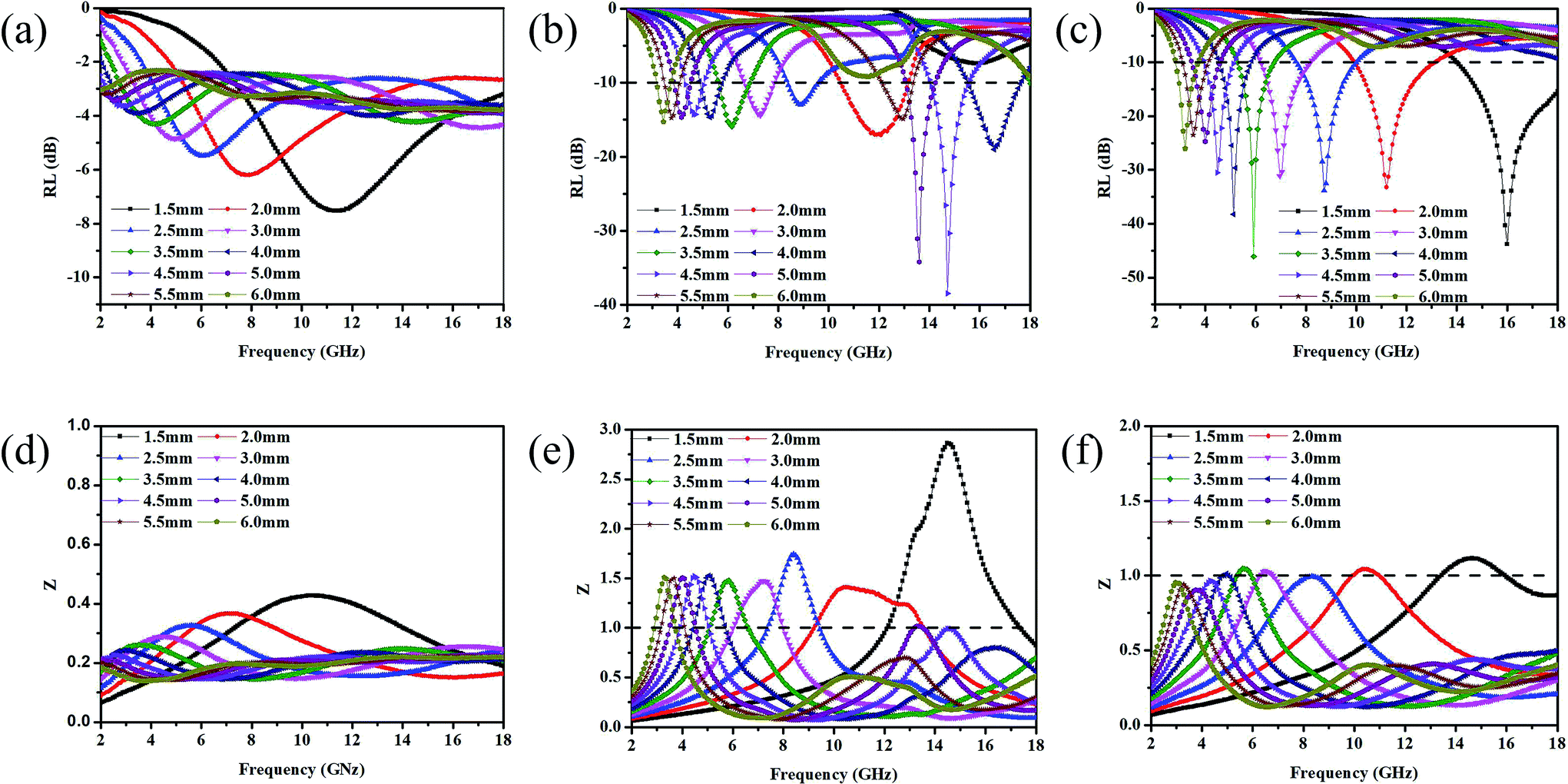
Fig. 8(a)–(c) shows the reflection loss values (RL) of GNs, Ni–P/GNs and Ni–Fe–P/GNs at different thicknesses and frequencies. We can see that the EM absorption peaks of the three groups of samples tend to move in the low frequency region as the thickness increases. The minimum reflection loss of GNs is only −7.5 dB at a thickness of 1.5 mm. It is generally considered that when the RL is less than −10 dB, the corresponding frequency is the effective EM absorption bandwidth of the material because when RL is less than −10 dB, more than 90% of incident electromagnetic waves are effectively absorbed.57,58 It can be seen that the EM wave absorption capacity of GNs of undeposited magnetic particles is relatively poor. From Fig. 8(b) it can be seen that Ni–P/GNs has an effective absorption bandwidth in the 2.0–6.0 mm thickness range. A minimum reflection loss of −38.4 dB is observed at a thickness of 4.5 mm, 14.7 GHz, and has an effective bandwidth of 2.3 GHz (4.3–5.1 GHz, 14.0–15.5 GHz) in total bandwidth. Its EM wave absorption capacity is much stronger than GNs. As shown in Fig. 8(c), the EM absorption capacity of Ni–Fe–P/GNs is better than that of Ni–P/GNs, and it has an effective absorption strength in the thickness range of 1.5 to 6.0 mm. It has a minimum reflection loss of −46.1 dB at 3.5 mm, 5.9 GHz and an effective bandwidth of 1.6 GHz (5.1–6.7 GHz). While it has a wider bandwidth of 4.0 GHz (14.0–18.0 GHz) at 1.5 mm, whose minimum reflection loss at 16.0 GHz is −43.8 GHz. In summary, Ni–Fe–P/GNs have a thinner thickness and stronger EM absorption capacity than Ni–P/GNs.
 | ||
| Fig. 8 Representation of RL values of the samples: (a) GNs, (b) Ni–P/GNs, and (c) Ni–Fe–P/GNs and the relationship between the normalized input impedance (Zin) and the frequency of (d) GNs, (e) Ni–P/GNs, and (f) Ni–Fe–P/GNs. | ||
Zin (impedance matching) in eqn (6) is one of the important indicators for measuring the EM wave absorbing properties of material. When Zin approaches Z0, that is the normalized input impedance of the absorber approaches the free-space impedance, it is effective to reduce the reflection of EM wave on the absorber surface and cause it to be converted and interfered in the absorber, which results in perfect impedance matching.59,60 This is manifested by the fact that the frequency at which Zin most approaches 1 is often the frequency at which the absorber exhibits the minimum reflection loss. To further investigate the relationship between RL and impedance, Fig. 8(d)–(f) is made according to eqn (6). As shown in Fig. 8(d), GNs with a thickness of 1.5 mm have a Z value of about 0.43 at 10.4 GHz, which is far from 1 and has poor impedance matching. The corresponding minimum reflection loss is also small. When Ni–P is introduced, as shown in Fig. 8(e), its Z value is higher than GNs, but most of them are also higher than 1. The Z value of Ni–P/GNs reaches 1 at 14.5 GHz at a thickness of 4.5 mm and reaches 1 at 13.4 GHz at a thickness of 5 mm, and the corresponding reflection loss also reaches a minimum at these two positions. The Z values of the remaining thicknesses are much higher than 1, so the impedance matching is not good, which also causes the absorber to exhibit poor absorbing ability at other thicknesses. As shown in Fig. 8(f), when Ni–Fe–P was introduced, the Z value of the absorber was remarkably improved, and the maximum Z value of all thicknesses in the range of 2–18 GHz was close to 1. The corresponding reflection loss is good, and the RL values are all lower than −20 dB. The Z value of Ni–Fe–P/GNs with a thickness of 3.5 mm is closest to 1 at 5.9 GHz, followed by Ni–Fe–P/GNs with a thickness of 1.5 mm at 16.0 GHz. Combined with its RL value, as shown in Fig. 8(c), We can see that the minimum reflection loss of the sample at 3.5 mm is −46.1 dB, which is greater than the −43.8 dB of the sample at 1.5 mm, which is consistent with the magnitude of its Z value. On the other hand, the Z curve of Ni–Fe–P/GN with a thickness of 3.5 mm is narrower than 1.5 mm, and the EM wave absorption bandwidth corresponding to Fig. 8(c) is also 3.5 mm narrower than 1.5 mm. This indicates that in addition to the number of Z values, its bandwidth in the range of 2–18 GHz is also closely related to the absorption bandwidth of the absorber. The above indicates that impedance matching is one of the important factors to improve the absorption performance of EM wave in Ni–Fe–P/GNs composites.
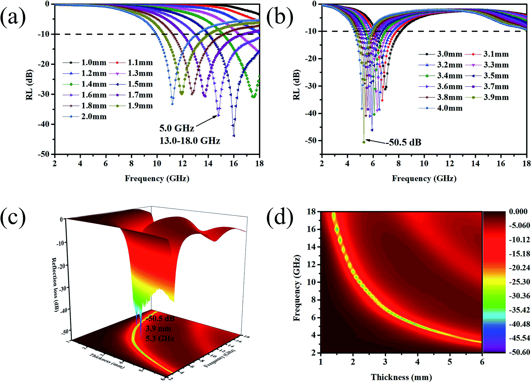
As can be seen from Fig. 8(c), Ni–Fe–P/GNs have excellent properties at thicknesses of 1.5 mm and 3.5 mm. We find the absorbing properties corresponding to the thicknesses around 1.5 mm and 3.5 mm and plot them as shown in Fig. 9(a) and (b). It was found that a minimum reflection loss of −50.5 dB was observed at 5.3 GHz when the thickness of the absorber was 3.9 mm. In addition, the effective absorption bandwidth (RL < 10 dB) of the absorber can reach 5.0 GHz (13.0–18.0 GHz) with a thickness of 1.6 mm. In order to intuitively observe the relationship between EM absorption performance, frequency and thickness, EM absorption properties (RL values) are shown with the frequency and thickness in Fig. 9(c) and (d) by a 3D color mapped wireframe surface and a contour, respectively. It can be clearly seen that the minimum RL in a certain thickness and frequency range can reach below −10 dB. This indicates that Ni–Fe–P/GNs can meet the requirements of modern absorbers, including low reflection loss, thin thickness, light weight and wide absorption frequency bandwidth.
 | ||
| Fig. 9 (a) RL values for Ni–Fe–P/GNs within 1.0–2.0 mm, (b) RL values for Ni–Fe–P/GNs within 3.0–4.0 mm, (c) the 3D color mapped wireframe surface of the RL values with different thickness and frequency, (d) a contour revealing the best performance for practical application. | ||
Table 1 shows a comparison of EM wave absorption properties of materials similar to Ni–Fe–P/GNs. The comparison results show that the EM wave absorption performance of Ni–Fe–P/GNs is excellent among similar products. The good EM wave absorption capacity of Ni–Fe–P/GNs can be attributed to the following explanation: (1) Ni–Fe–P as a magnetic loss absorber is deposited on the GNs surface, thereby improving impedance matching. The addition of Ni–Fe–P improves the impedance matching better than Ni–P, which is why Ni–Fe–P/GNs has a stronger EM absorption capability. As we all know, good impedance matching is one of the most important factors affecting the EM wave absorption of material. (2) The introduction of magnetic particles causes the composite to have multiple interfaces, thereby causing interfacial polarization to cause multiple scattering of incident EM waves. (3) The deposition of magnetic particles increases the surface defects of the graphene nanosheets, and the resulting dipole polarization will promote the absorption of EM waves. (4) A conductive network composed of Ni–Fe–P particles and GNs flakes can cause natural resonance, causing incident EM wave to dissipate through dielectric loss and magnetic loss mechanisms.35
| Fillers in paraffin | Minimum RL (frequency) | Effective bandwidth (GHz) (RL < −10 dB) | Thickness (mm) | Ref. |
|---|---|---|---|---|
| Hexagonal Ni/graphene | −17.8 dB | 5.0 | 23 | |
| Ni/graphene | −23.3 dB (7.5 GHz) | 1.8 | 3.0 | 61 |
| Urchinlike Ni/RGO | −32.1 dB (13.8 GHz) | 4.5 | 2.0 | 62 |
| Graphene@Ni@C | −34.2 dB (13.9 GHz) | 3.2 | 1.6 | 25 |
| Fe50Ni50/graphene | −23.9 dB (10.8 GHz) | 4.3 | 3.0 | 26 |
| Fe@Ni/graphene/epoxy | −22.7 dB (14.9 GHz) | 5.5 | 2.0 | 27 |
| Ni–P/GNs | −38.4 dB (14.7 GHz) | 2.3 | 4.5 | This work |
| Ni–Fe–P/GNs | −50.5 dB (16.0 GHz) | 1.3 | 3.9 | This work |
| −37.0 dB (14.8 GHz) | 5.0 | 1.6 |
4. Conclusion
In summary, we successfully introduced Fe into Ni–P/GNs composite by one-step hydrothermal method, and prepared composites material of Ni–Fe–P microspheres decorated with GNs (graphene nanosheets) with excellent EM wave absorption properties. Studies have shown that the introduction of Fe reduces the reduction rate of Ni2+ and makes it difficult to nucleate and grow Ni. Under the same experimental conditions, the particle size of Ni–Fe–P microspheres is smaller than that of Ni–P, and the distribution on the graphene nanosheets is also sparse than the Ni–P microspheres. In terms of EM wave absorption, the introduction of Fe greatly improves the absorption performance of Ni–P/GNs, with a minimum reflection loss of −50.5 dB, occurring at 5.3 GHz and a thickness of 3.9 mm. While the thickness of only 1.6 mm has the widest effective absorption bandwidth of 5.0 GHz (13.0–18.0 GHz). The enhanced EM wave absorption performance is mainly due to the fact that the introduction of Fe enhances the synergistic effect between dielectric loss and magnetic loss, thereby improving impedance matching. In addition, in the process of preparing the composite material, the time of the graphene nanosheets is shorter than the conventional graphene oxide, which is advantageous for industrial production. In summary, Ni–Fe–P/GNs can be a promising EM wave absorber.Conflicts of interest
There are no conflicts to declare.Acknowledgements
This work was supported by National Natural Science Foundation of China (51772060, 51672059, 51621091, 51372052, and 51021002).References
- Q. Song, F. Ye, X. Yin, W. Li, H. Li, Y. Liu, K. Li, K. Xie, X. Li and Q. Fu, Adv. Mater., 2017, 29, 1701583 CrossRef PubMed.
- D. Zhang, F. Xu, J. Lin, Z. Yang and M. Zhang, Carbon, 2014, 80, 103–111 CrossRef CAS.
- B. Zhao, X. Guo, W. Zhao, J. Deng, G. Shao, B. Fan, Z. Bai and R. Zhang, ACS Appl. Mater. Interfaces, 2016, 8, 28917–28925 CrossRef CAS PubMed.
- H. Zhang, M. Hong, P. Chen, A. Xie and Y. Shen, J. Alloys Compd., 2016, 665, 381–387 CrossRef CAS.
- M. Chen, H. Zhang, G. Zeng, D. Zhang, C. Yan, Y. Shen, X. Yu, Q. Wu and Y. Chen, RSC Adv., 2017, 7, 38549–38556 RSC.
- D. Micheli, R. Pastore, G. Gradoni, V. Mariani Primiani, F. Moglie and M. Marchetti, Acta Astronaut., 2013, 88, 61–73 CrossRef CAS.
- Z. Chen, C. Xu, C. Ma, W. Ren and H. M. Cheng, Adv. Mater., 2013, 25, 1296–1300 CrossRef CAS PubMed.
- W.-L. Song, M.-S. Cao, M.-M. Lu, J. Liu, J. Yuan and L.-Z. Fan, J. Mater. Chem. C, 2013, 1, 1846 RSC.
- Z. Zhu, Nano-Micro Lett., 2017, 9, 25 CrossRef PubMed.
- L. Kong, X. Yin, X. Yuan, Y. Zhang, X. Liu, L. Cheng and L. Zhang, Carbon, 2014, 73, 185–193 CrossRef CAS.
- B. Zhao, G. Shao, B. Fan, Y. Xie and R. Zhang, J. Magn. Magn. Mater., 2014, 372, 195–200 CrossRef CAS.
- P. Liu, Y. Huang and X. Zhang, Synth. Met., 2015, 201, 76–81 CrossRef CAS.
- S. Acharya, J. Ray, T. U. Patro, P. Alegaonkar and S. Datar, Nanotechnology, 2018, 29, 115605 CrossRef PubMed.
- Y. Xu, Q. Wang, Y. Cao, X. Wei and B. Huang, RSC Adv., 2017, 7, 18172–18177 RSC.
- P. Liu, Y. Huang, J. Yan, Y. Yang and Y. Zhao, ACS Appl. Mater. Interfaces, 2016, 8, 5536–5546 CrossRef CAS PubMed.
- M. Han, X. Yin, Z. Hou, C. Song, X. Li, L. Zhang and L. Cheng, ACS Appl. Mater. Interfaces, 2017, 9, 11803–11810 CrossRef CAS PubMed.
- P. Liu, Y. Huang, J. Yan and Y. Zhao, J. Mater. Chem. C, 2016, 4, 6362–6370 RSC.
- S. Han, S. Wang, W. Li, Y. Lai, N. Zhang, N. Yang, Q. Wang and W. Jiang, Ceram. Int., 2018, 44, 10352–10361 CrossRef CAS.
- L. Xiong, M. Yu, J. Liu, S. Li and B. Xue, RSC Adv., 2017, 7, 14733–14741 RSC.
- W. Ye, J. Fu, Q. Wang, C. Wang and D. Xue, J. Magn. Magn. Mater., 2015, 395, 147–151 CrossRef CAS.
- Y. Wang, X. Wu, W. Zhang, C. Luo and J. Li, J. Magn. Magn. Mater., 2017, 443, 358–365 CrossRef CAS.
- Y. Chen, Z. Lei, H. Wu, C. Zhu, P. Gao, Q. Ouyang, L.-H. Qi and W. Qin, Mater. Res. Bull., 2013, 48, 3362–3366 CrossRef CAS.
- T. Chen, F. Deng, J. Zhu, C. Chen, G. Sun, S. Ma and X. Yang, J. Mater. Chem., 2012, 22, 15190 RSC.
- J. Fang, W. Zha, M. Kang, S. Lu, L. Cui and S. Li, J. Mater. Sci., 2013, 48, 8060–8067 CrossRef CAS.
- C. Li, Y. Huang and J. Chen, Mater. Lett., 2015, 154, 136–139 CrossRef CAS.
- J. Wang, J. Wang, R. Xu, Y. Sun, B. Zhang, W. Chen, T. Wang and S. Yang, J. Alloys Compd., 2015, 653, 14–21 CrossRef CAS.
- B. Zhang, J. Wang, H. Tan, X. Su, S. Huo, S. Yang, W. Chen and J. Wang, J. Mater. Sci.: Mater. Electron., 2017, 29, 3348–3357 CrossRef.
- D. Moitra, M. Chandel, B. K. Ghosh, R. K. Jani, M. K. Patra, S. R. Vadera and N. N. Ghosh, RSC Adv., 2016, 6, 76759–76772 RSC.
- R. Shu, W. Li, X. Zhou, D. Tian, G. Zhang, Y. Gan, J. Shi and J. He, J. Alloys Compd., 2018, 743, 163–174 CrossRef CAS.
- X.-J. Zhang, G.-S. Wang, W.-Q. Cao, Y.-Z. Wei, J.-F. Liang, L. Guo and M.-S. Cao, ACS Appl. Mater. Interfaces, 2014, 6, 7471–7478 CrossRef CAS PubMed.
- L. Wan, J. Zhang, Y. Chen, H. Wang, W. Hu, L. Liu and Y. Deng, J. Phys. D: Appl. Phys., 2015, 48, 355302 CrossRef.
- Y. Tan, D. Sun, H. Yu, T. Wu, B. Yang, Y. Gong, S. Yan, R. Du, Z. Chen and X. Xing, J. Alloys Compd., 2014, 605, 230–236 CrossRef CAS.
- M. R. Ammar, N. Galy, J. N. Rouzaud, N. Toulhoat, C. E. Vaudey, P. Simon and N. Moncoffre, Carbon, 2015, 95, 364–373 CrossRef CAS.
- B. Li, L. Zhou, D. Wu, H. Peng, K. Yan, Y. Zhou and Z. Liu, ACS Nano, 2011, 5, 5957–5961 CrossRef CAS PubMed.
- Y. Lai, S. Wang, D. Qian, S. Zhong, Y. Wang, S. Han and W. Jiang, Ceram. Int., 2017, 43, 12904–12914 CrossRef CAS.
- H. Wang, H. Guo, Y. Dai, D. Geng, Z. Han, D. Li, T. Yang, S. Ma, W. Liu and Z. Zhang, Appl. Phys. Lett., 2012, 101, 083116 CrossRef.
- T. K. Gupta, B. P. Singh, S. R. Dhakate, V. N. Singh and R. B. Mathur, J. Mater. Chem. A, 2013, 1, 9138 RSC.
- B. Zhao, W. Zhao, G. Shao, B. Fan and R. Zhang, ACS Appl. Mater. Interfaces, 2015, 7, 12951–12960 CrossRef CAS PubMed.
- Z. Zhu, X. Sun, G. Li, H. Xue, H. Guo, X. Fan, X. Pan and J. He, J. Magn. Magn. Mater., 2015, 377, 95–103 CrossRef CAS.
- X. Sun, J. He, G. Li, J. Tang, T. Wang, Y. Guo and H. Xue, J. Mater. Chem. C, 2013, 1, 765–777 RSC.
- L. Yan, J. Wang, X. Han, Y. Ren, Q. Liu and F. Li, Nanotechnology, 2010, 21, 095708 CrossRef PubMed.
- D. Ding, Y. Wang, X. Li, R. Qiang, P. Xu, W. Chu, X. Han and Y. Du, Carbon, 2017, 111, 722–732 CrossRef CAS.
- K. Zhang, X. Gao, Q. Zhang, T. Li, H. Chen and X. Chen, J. Alloys Compd., 2017, 721, 268–275 CrossRef CAS.
- S. L. Wen, Y. Liu, X. C. Zhao and J. W. Cheng, J. Appl. Phys., 2014, 116, 054310 CrossRef.
- P. Yang, Y. Liu, X. Zhao, W. Chen and C. Zhang, J. Mater. Sci.: Mater. Electron., 2018, 29, 2455–2462 CrossRef CAS.
- J. Feng, Y. Hou, Y. Wang and L. Li, ACS Appl. Mater. Interfaces, 2017, 9, 14103 CrossRef CAS PubMed.
- S. He, G.-S. Wang, C. Lu, J. Liu, B. Wen, H. Liu, L. Guo and M.-S. Cao, J. Mater. Chem. A, 2013, 1, 4685 RSC.
- B. Zhao, G. Shao, B. Fan, C. Wang, Y. Xie and R. Zhang, Powder Technol., 2015, 270, 20–26 CrossRef CAS.
- X.-J. Zhang, G.-S. Wang, Y.-Z. Wei, L. Guo and M.-S. Cao, J. Mater. Chem. A, 2013, 1, 12115 RSC.
- M. Yu, P. Yang, J. Fu, S. Liu and S. Qi, Smart Mater. Struct., 2016, 25, 085046 CrossRef.
- M. Yu, L. Wang, P. Yang and J. Fu, Nanotechnology, 2017, 28, 485703 CrossRef PubMed.
- B. Zhao, G. Shao, B. Fan, B. Sun, K. Guan and R. Zhang, J. Mater. Sci.: Mater. Electron., 2014, 25, 3614–3621 CrossRef CAS.
- B. Zhao, G. Shao, B. Fan, W. Zhao, Y. Xie and R. Zhang, J. Mater. Chem. A, 2015, 3, 10345–10352 RSC.
- N. Li, G. W. Huang, Y. Li, H. M. Xiao, Q. P. Feng, N. Hu and S. Y. Fu, ACS Appl. Mater. Interfaces, 2017, 9, 2973–2983 CrossRef CAS PubMed.
- B. Dai, B. Zhao, X. Xie, T. Su, B. Fan, R. Zhang and R. Yang, J. Mater. Chem. C, 2018, 6, 5690–5697 RSC.
- J. Ma, X. Wang, W. Cao, C. Han, H. Yang, J. Yuan and M. Cao, Chem. Eng. J., 2018, 339, 487–498 CrossRef CAS.
- Y. Li, Y. Zhao, X. Lu, Y. Zhu and L. Jiang, Nano Res., 2016, 9, 2034–2045 CrossRef CAS.
- L. Tian, X. Yan, J. Xu, P. Wallenmeyer, J. Murowchick, L. Liu and X. Chen, J. Mater. Chem. A, 2015, 3, 12550–12556 RSC.
- Y. Du, W. Liu, R. Qiang, Y. Wang, X. Han, J. Ma and P. Xu, ACS Appl. Mater. Interfaces, 2014, 6, 12997–13006 CrossRef CAS PubMed.
- B. Zhong, Y. Cheng, M. Wang, Y. Bai, X. Huang, Y. Yu, H. Wang and G. Wen, Composites, Part A, 2018, 112, 515–524 CrossRef CAS.
- X. Wang, M. Yu, W. Zhang, B. Zhang and L. Dong, Appl. Phys. A: Mater. Sci. Process., 2014, 118, 1053–1058 CrossRef.
- G. Liu, W. Jiang, D. Sun, Y. Wang and F. Li, Appl. Surf. Sci., 2014, 314, 523–529 CrossRef CAS.
| This journal is © The Royal Society of Chemistry 2019 |