DOI:
10.1039/C8RA10363A
(Paper)
RSC Adv., 2019,
9, 10584-10598
Leakage-free solution-processed organic light-emitting diode using a ternary host with single-diode emission area up to 6 × 11.5 cm2†
Received
18th December 2018
, Accepted 10th March 2019
First published on 4th April 2019
Abstract
The electrical current leakage and stability are studied for solution-processed OLEDs with areas of 4.45 mm2, 3 × 3.2 cm2, and 6 × 11.5 cm2. The emission layer of the OLED has a ternary or binary mixed host with hole-transporting molecules tris(4-carbazoyl-9-ylphenyl)amine (TCTA) and 9-(4-tert-butylphenyl)-3,6-bis(triphenylsilyl)-9H-carbazole (CzSi), together with the electron-transporting molecule 2,7-bis(diphenylphosphoryl)-9,9′-spirobi[fluorene] (SPPO13). The phosphorescent emitters are Ir(mppy)3 for green and bis[4-(4-tert-butylphenyl)thieno[3,2-c]pyridine][N,N′-diisopropylbenamidinato]iridium(III) (PR-02) for orange. Poly[(9,9-dioctylfluorenyl-2,7-diyl)-co-(4,4′-(N-(4-sec-butylphenyl))diphenylamine)] (TFB) is used as the hole transport layer and PEDOT:PSS is used as the hole injection layer. On top of the emission layer, CsF/Al is deposited by thermal evaporation as the cathode. All organic layers are deposited by blade coating and the initial current leaking defects can be avoided by careful control of the coating conditions. The detrimental burning point caused by a local current short developed after long-time operation can be avoided by reducing the operation voltage using a ternary mixed host. The operation voltage is only 4 V at 100 cd m−2 and 5 V at 250 cd m−2 for the green emitting device. Furthermore, the crystallization defect is reduced by the ternary host. For the orange emitting device, the binary host is good enough with an operating voltage of 5 V at 100 cd m−2. For an area as large as 6 × 11.5 cm2, the OLED shows good stability and there is no burning point after an operation of over 1600 hours.
Introduction
In addition to the information display, the organic light-emitting diode (OLED) has a great potential to be applied in the lighting technology. There are two sectors for the lighting; one is the high-brightness white light for the primary lighting and another is the low brightness supporting light for design with all colors. For the design lighting, inorganic LEDs are now the dominating technology, but they have the disadvantages of being point-like, hot, unnatural in color, and harmful to human eyes. On the other hand, the OLED has the unique features of flatness, low heat generation, and comfortable color to humans. Unlike displays, lighting products are highly sensitive to the cost per unit area. The vacuum deposition process for the OLED fabrication, successful for fabricating displays, is therefore not ultimately competitive for lighting due to the intrinsically high cost. One of the greatest challenges for the application of low-cost solution-processed OLEDs in lighting is the electrical current leakage caused by the point defects. Unlike the case of displays, where the OLEDs are made into a matrix with very fine individual pixels, in lighting, the product is ideally made with one large diode without pixels. In the case of a pixel matrix, all of the small OLEDs are individually driven. Using this approach, the product as a whole survives if there is a current short in one pixel. However for a single large diode, the current short due to any defect within the active area will cause the complete failure of the entire product. In practice, the emitting area of a single OLED for lighting is expected to be in the range of 3 × 3 to 10 × 10 cm2. Although a fine matrix can still be made for lighting, such fabrication leads to a high cost, which is incompatible with the low-cost demands for lighting in general. In addition, the matrix design implies a complicated driving circuit such that each pixel can be individually addressed. Therefore, the success of OLED lighting technology depends on devising a way to prevent a single electrical leakage causing defect for large areas over 10 cm2, such that the OLED can be made as a low-cost large single diode driven simply by a converter or a battery like a conventional light bulb. There are reports on the large-area OLED prepared by solution and vacuum processes,1–3 and the all-solution processed OLED with pixels.4 However, there are few reports in the literature so far on the formation of the current-leaking defects and the ways to prevent current leakage in a large-area all-solution processed OLED as a single diode.
Point defects may come from each step of the fabrication for solution-processed OLEDs. Some, but not all of them, are listed as follows: etching defect in indium-tin-oxide (ITO) glass, aggregation in the hole injection layer of poly(3,4-ethylenedioxythiophene)-poly(styrenesulfonate) (PEDOT:PSS), the crystallization of the small-molecule organic semiconductors, the dust particles, and the unevenness of the electron injection salt (e.g. LiF or CsF in cathode evaporation). In this work, we show that the defects in ITO, PEDOT:PSS, and semiconductor layers can be prevented by careful control of the solution deposition conditions using blade coating.5–10 However, the current leakage caused by the cathode, called the burning point, is extremely sensitive to the voltage and inevitable after long-time operations if the OLED operation voltage is high. Since mixed-host OLEDs have demonstrated better performance and lifetime,11–15 in this work, we demonstrate that by using a ternary mixed host of the small molecules, the operation voltage can be reduced relative to the conventional binary mixed host. The possible reason is the prevention of the formation of micro-crystals, which may form charge carrier traps in an otherwise amorphous film. The crystallization might become less likely as there are more components in the mixture.
The operation voltage at 200 cd m−2 is only 4 V using a ternary mixed phosphorescent host, which is significantly lower than the voltage of 5 V for the similar binary host. The ternary host contains two hole-transport molecules and one electron-transport molecule. Right after the fabrication, the current efficiencies for the large OLEDs with emission areas of 3 × 3.2 cm2 and 6 × 11.5 cm2 were close to the small OLED with an area of 4.45 mm2 for a given luminance. Because the point defect for a small area can be ruled out, the similar initial current efficiency indicates that most of the leakage defects are avoided. After a long-time operation, the large OLED develops burning points if the binary host is used for the green phosphorescent device. On the other hand, not a single burning point develops when the ternary host is used, even after a continuous operation of up to 1600 hours with an emission area as large as 6 × 11.5 cm2. Such stability appears to meet the basic criterion for the commercial application of OLEDs for design lighting at a moderate brightness of around 30–200 cd m−2.
Experimental
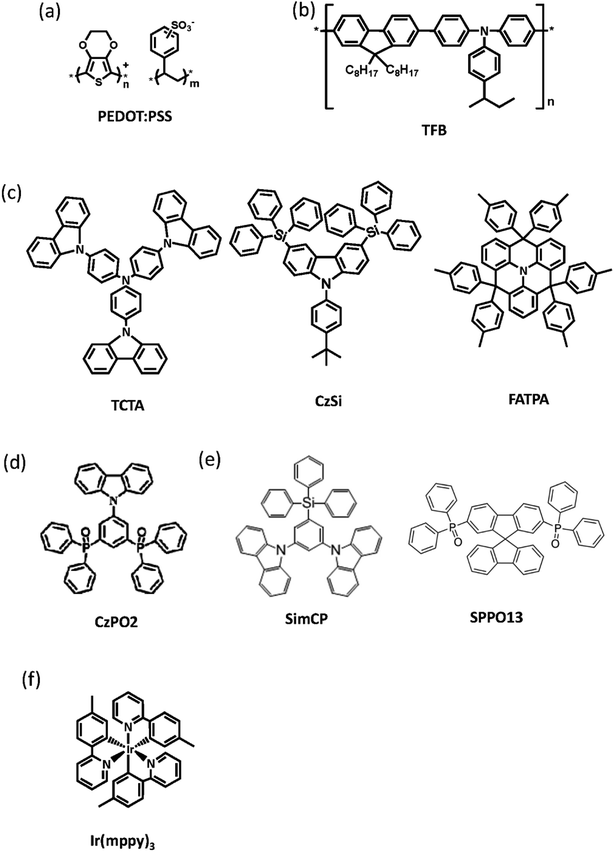
The full names and abbreviations of the organic materials used in this work are listed below. The chemical structures of these organic materials are shown in Fig. 2 and 5(a). These materials are poly(3,4-ethylenedioxy-thiophene):poly(styrenesulfonate) (PEDOT:PSS, CLEV-IOS™ P VP CH8000, purchased from HC Starck), poly[(9,9-dioctylfluorenyl-2,7-diyl)-co-(4,4′-(N-(4-sec-butylphenyl))diphenylamine)] (TFB, Xi'an Polymer Light Technology Corp.), 4,4′,4′′-Tris(carbazol-9-yl)triphenylamine (TCTA), 9-(4-tert-butylphenyl)-3,6-bis(triphenylsilyl)-9H-carbazole (CzSi), 4,4,8,8,-12,12-hexa-p-tolyl-4H-8H-12H-12C-aza-dibenzo[cd,mn]pyrene (FATPA), 9-(3,5-bis(diphenylphosphoryl)phenyl)-9H-carbazole (CzPO2), 9,9′-(5-(triphenylsilyl)-1,3-phenylene)bis(9H-carbazole) (SimCP), 2,7-bis(diphenylphosphoryl)-9,9′-spirobifluorene (SPPO13), and Tris[2-(p-tolyl)pyridine]iridium(III) (Ir(mppy)3). TCTA, CzSi, FATPA, CzPO2, SimCP, SPPO13 and Ir(mppy)3 were purchased from Luminescence Technology Corp., Ltd. PR-02 was provided by the Dept. of Organic Light Emitting Materials Device Research, Industrial Technology Research Institute.
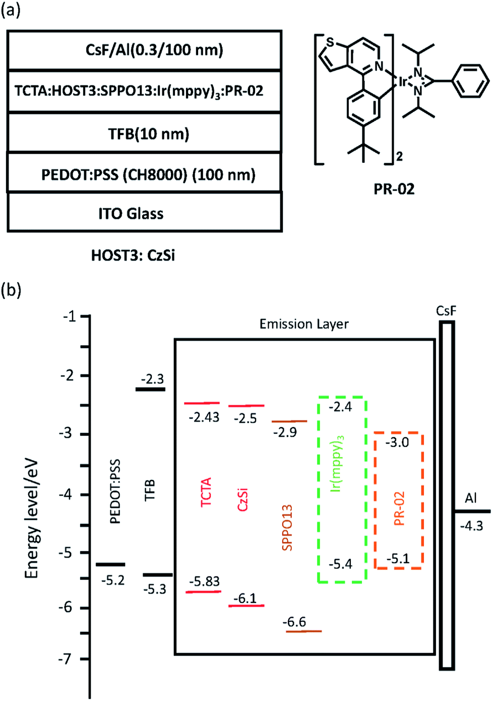
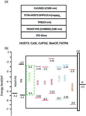
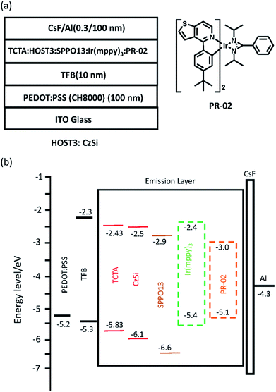
In this study, we used a blade coating process to fabricate the organic layer. We added an organic solution dropwise between the blade (30–120 μm gaps) and the substrate using a micropipette. The blade was driven by a linear motor on the substrate through capillary action forming the wet film. We then used a hotplate under the substrate and hot air above the blade to dry the wet film.5–10 The organic thin films were fabricated via the following steps to complete our devices. First, we diluted PEDOT:PSS (CH8000) in ethanol (1![[thin space (1/6-em)]](https://www.rsc.org/images/entities/char_2009.gif) :2.5 v/v). After blade coating PEDOT:PSS on the indium tin oxide (ITO) substrate, we baked this thin film at 150 °C for 15 min in air. The organic film formed the active areas with an area of 4.45 mm2, 3.2 cm × 3.0 cm (960 mm2), 6.0 cm × 11.5 cm, and the thickness was ca. 100 nm. Second, we dissolved TFB in toluene and blade coated on PEDOT:PSS, followed by baking at 180 °C in air for 40 min. The substrate was transferred to a glove box for fabricating the emitting layer. For the green PhOLED, the three host and one emitter materials were TCTA, CzSi, SPPO13 and Ir(mppy)3as the emission layer (EML), respectively. For the orange PhOLED, the three host materials and two emitter materials were TCTA, CzSi, SPPO13, Ir(mppy)3 and PR-02 as the emission layer (EML), respectively. These materials were dissolved in chloroform (1 wt%). The blend ratios are PR-02:Ir(mppy)3:TCTA:CzSi:SPPO13 = 3:14:29.05:12.45:41.5 and Ir(mppy)3:TCTA:CzSi:SPPO13 = 6:13.4:13.4:67. The EML was fabricated by blade-coating and then heated at 80 °C for 10 min; the thickness was ca. 60 nm. We used thermal evaporation to deposit the CsF (0.3 nm) and Al (100 nm) as the top electrode under 3 × 10⁻⁶ torr. Finally, we applied the sealant Moisture Cut WB90US (P) (MORESCO Corporation) on the sandblasted glass covering the active area of the device. We used a power supply (Keithley 2400) to measure the device current and voltage, and a spectroradiometer (PR655) to measure the luminance. The device structure was ITO/PEDOT:PSS (ca. 100 nm)/TFB (ca. 10 nm)/EML (ca. 60 nm)/CsF (0.3 nm)/Al (100 nm), which is shown in Fig. 1(a) and 5(a). The energy level diagram is shown in Fig. 1(b) and 5(b).
:2.5 v/v). After blade coating PEDOT:PSS on the indium tin oxide (ITO) substrate, we baked this thin film at 150 °C for 15 min in air. The organic film formed the active areas with an area of 4.45 mm2, 3.2 cm × 3.0 cm (960 mm2), 6.0 cm × 11.5 cm, and the thickness was ca. 100 nm. Second, we dissolved TFB in toluene and blade coated on PEDOT:PSS, followed by baking at 180 °C in air for 40 min. The substrate was transferred to a glove box for fabricating the emitting layer. For the green PhOLED, the three host and one emitter materials were TCTA, CzSi, SPPO13 and Ir(mppy)3as the emission layer (EML), respectively. For the orange PhOLED, the three host materials and two emitter materials were TCTA, CzSi, SPPO13, Ir(mppy)3 and PR-02 as the emission layer (EML), respectively. These materials were dissolved in chloroform (1 wt%). The blend ratios are PR-02:Ir(mppy)3:TCTA:CzSi:SPPO13 = 3:14:29.05:12.45:41.5 and Ir(mppy)3:TCTA:CzSi:SPPO13 = 6:13.4:13.4:67. The EML was fabricated by blade-coating and then heated at 80 °C for 10 min; the thickness was ca. 60 nm. We used thermal evaporation to deposit the CsF (0.3 nm) and Al (100 nm) as the top electrode under 3 × 10⁻⁶ torr. Finally, we applied the sealant Moisture Cut WB90US (P) (MORESCO Corporation) on the sandblasted glass covering the active area of the device. We used a power supply (Keithley 2400) to measure the device current and voltage, and a spectroradiometer (PR655) to measure the luminance. The device structure was ITO/PEDOT:PSS (ca. 100 nm)/TFB (ca. 10 nm)/EML (ca. 60 nm)/CsF (0.3 nm)/Al (100 nm), which is shown in Fig. 1(a) and 5(a). The energy level diagram is shown in Fig. 1(b) and 5(b).
 |
| | Fig. 1 (a) Device structure, and (b) schematic of the energy level of the green phosphorescent OLED with ternary host materials. | |
 |
| | Fig. 2 Molecular structures of the organic materials of the green PhOLED device used in this work. (a) Conductive material PEDOT:PSS; (b) and (c) were hole transporting materials TFB, TCTA, CzSi, and FATPA; (d) electron transporting material CzPO2; (e) bipolar host materials SimCP and SPPO13; (f) green emissive material Ir(mppy)3. | |
Results and discussion
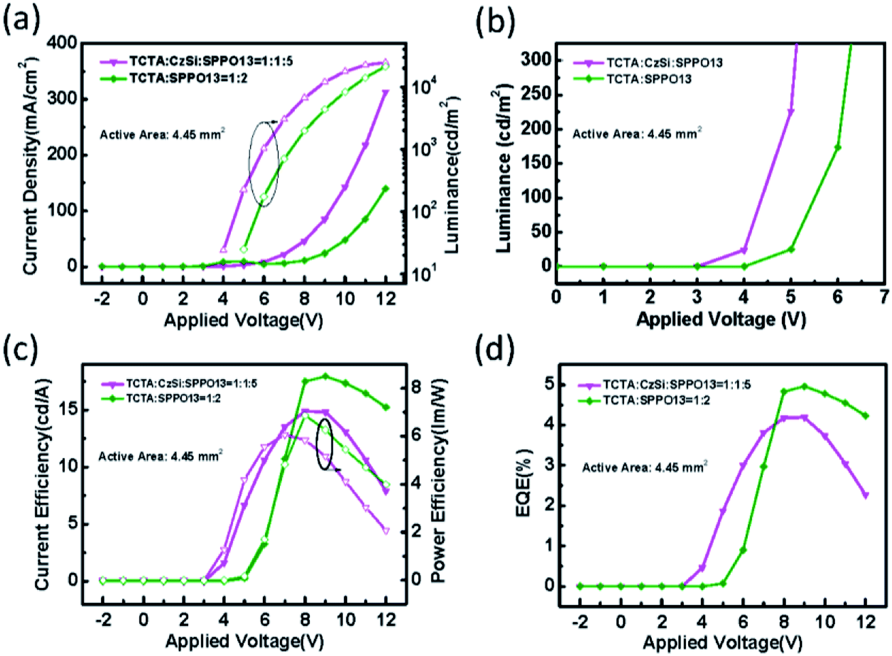
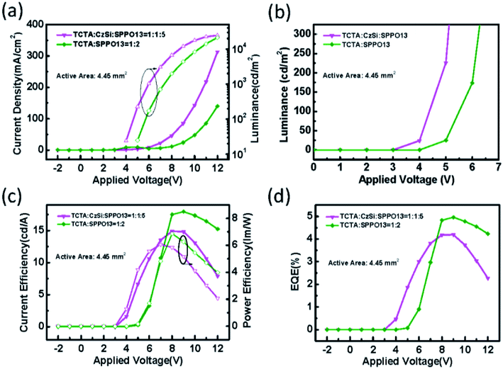
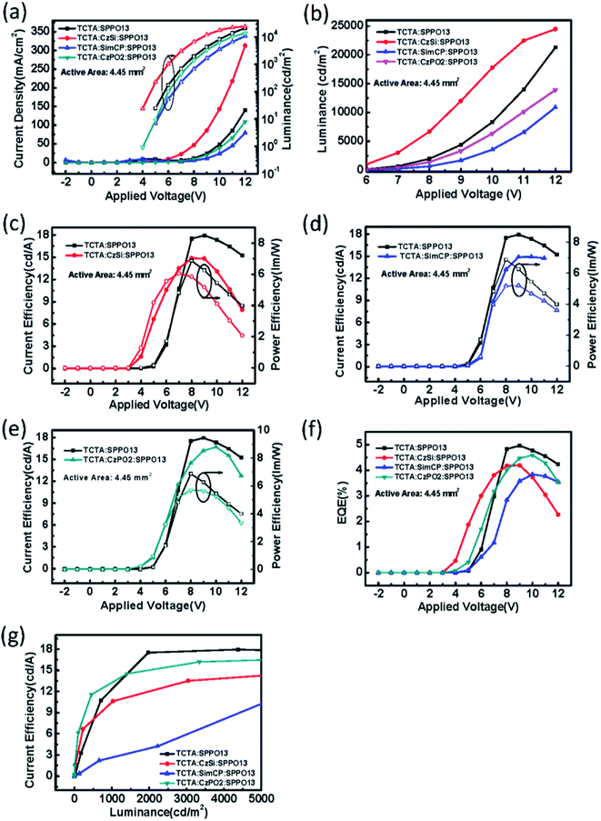
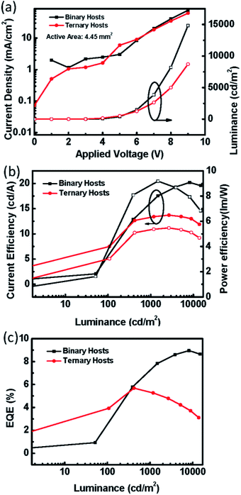
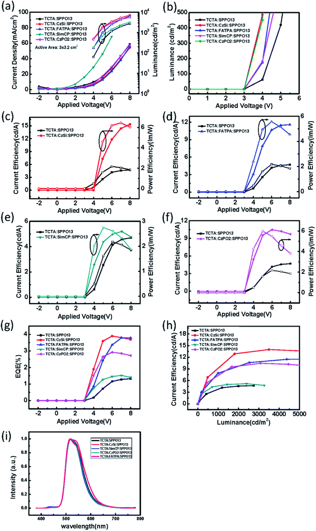
First, we prepared a phosphorescent OLED with an active area of 4.45 mm2 to understand the binary and ternary systems. In the solution process, the host material may lead to crystallization in the organic film. The mixed emission layer with multiple host materials not only allowed for charge balance, but also prevented crystallization in the organic film, thus improving the device stability. In order to investigate the intrinsic behavior of the third host in the emission layer of the ternary system, we compared a binary host system with the ternary host system. A variety of blending ratios were investigated in the binary and ternary host systems, as shown in Fig. S1.† The host film composed of TCTA:SPPO13 = 1:2 showed uniform morphology without any defects, while the films of other ratios showed a few defects (Fig. S1(a)†). The ternary host film composed of TCTA:CzSi:SPPO13 = 1:1:5 also showed uniform morphology. Since the devices with the binary host (TCTA:SPPO13 = 1:2) and ternary host (TCTA:CzSi:SPPO13 = 1:1:5) showed best performances (Fig. S1(b–g)†), we investigated and compared these devices in the following study. The electrical properties of the binary OLED and ternary OLED with an emission layer of 100 nm are shown in Fig. 3(a–d). The statistics of the device performance are shown in Table 1. In Fig. 3(a), it can be seen that the applied voltage of the ternary OLED is clearly lower than that for the binary OLED for a luminance of 1000 cd m−2. Therefore, the emission layer containing the ternary host material effectively reduced the operating voltage, which would be beneficial for large-area OLEDs. The addition of CzSi might have some advantages. First, the LUMO level of −2.5 eV may facilitate the electron injection and transportation. Second, the hole mobility of 5 × 10⁻⁵ cm2 V−1 s−1 may facilitate the hole transportation. We used CzSi as the host material, which contains a Cz group and Si atoms. Then, SimCP and CzPO2 were selected for comparison as they contain Si and Cz, respectively. We fixed the thickness of the emission layer to 100 nm with the two host materials SimCP and CzPO2, in order to compare their electrical properties. The electrical properties of the ternary OLED with different host compositions are shown in Fig. 4(a–e). As is evident from Fig. 4(a), the devices with SimCP and CzPO2 did not show a decrease in their operating voltages. This was possibly because SimCP and CzPO2 could not decrease the turn-on voltage in the multi-host system, as the bipolar properties were not advantageous for the device with a ternary host. Further, we attempted to understand whether the ternary system can be applied to an orange phosphorescent OLED (PhOLED). We applied the optimal composition of the emission layer in this study to an orange emitting device. The device structure and energy band diagram of the orange PhOLED are shown in Fig. 5(a) and (b), respectively. The molecular chemical structure of PR-02 is shown in Fig. 5(a) and was used as the emitter. As seen in Fig. 6(a), the I–V curve did not indicate a reduction in the operating voltage. The electrical performance of the device with a ternary host did not surpass that of the device with a binary host. Therefore, CzSi may not be suitable for the PR-02 system.
 |
| | Fig. 3 (a) The current density (solid symbols) and luminance (open symbols) versus applied voltage, (b) luminance versus applied voltage, (c) the current efficiency (solid symbols) and power efficiency (open symbols) versus applied voltage, (d) the EQE of the ternary OLED devices with different EML thicknesses. | |
 |
| | Fig. 4 (a) The current density (solid symbols) and luminance (open symbols) versus applied voltage; (b) luminance versus applied voltage; the current efficiency (solid symbols) and power efficiency (open symbols) versus applied voltage of the device added with (c) CzSi, (d) SimCP, (e) and CzPO2; (f) the EQE versus applied voltage; (g) the current efficiency versus luminance of the binary OLED devices and the ternary OLED devices with different third host materials CzSi, SimCP, and CzPO2. | |
 |
| | Fig. 5 (a) Device structure and molecular structure of PR-02, and (b) schematic of the energy level of the orange phosphorescent OLED with ternary host materials. | |
Table 1 Statistics of device performance
| Device |
Applied voltage (V) |
Current efficiency (cd A−1) |
Power efficiency (lm W−1) |
EQE (%) |
| Ir:TCTA:SPPO13 |
6 |
3.69 ± 3.6 |
1.93 ± 1.9 |
1.06 ± 1.0 |
| 7 |
5.00 ± 4.9 |
2.24 ± 2.2 |
1.44 ± 1.4 |
| 8 |
6.30 ± 5.7 |
2.47 ± 2.2 |
1.82 ± 1.6 |
| Ir:TCTA:FATPA:SPPO13 |
6 |
7.92 ± 1.9 |
4.15 ± 1.0 |
2.27 ± 0.7 |
| 7 |
8.25 ± 2.3 |
3.70 ± 1.0 |
2.55 ± 0.7 |
| 8 |
8.02 ± 2.5 |
3.15 ± 1.0 |
2.52 ± 0.7 |
| Ir:TCTA:CzSi:SPPO13 |
6 |
11.74 ± 2.5 |
6.06 ± 1.5 |
3.27 ± 0.7 |
| 7 |
14.32 ± 1.7 |
6.32 ± 1.0 |
4.00 ± 0.5 |
| 8 |
15.26 ± 2.7 |
5.90 ± 1.2 |
4.26 ± 0.7 |
| Ir:TCTA:CzPO2:SPPO13 |
6 |
6.00 ± 3.3 |
3.14 ± 1.7 |
1.72 ± 0.9 |
| 7 |
8.05 ± 2.1 |
3.61 ± 1.0 |
2.31 ± 0.6 |
| 8 |
9.48 ± 1.3 |
3.72 ± 0.5 |
2.73 ± 0.4 |
| Ir:TCTA:SimCP:SPPO13 |
6 |
2.77 ± 1.5 |
1.45 ± 0.8 |
0.82 ± 0.5 |
| 7 |
4.82 ± 1.9 |
2.16 ± 0.9 |
1.43 ± 0.6 |
| 8 |
7.13 ± 3.0 |
2.80 ± 1.2 |
2.10 ± 0.9 |
 |
| | Fig. 6 (a) The current density (solid symbols) and luminance (open symbols) versus applied voltage, (b) the current efficiency (solid symbols) and power efficiency (open symbols) versus luminance, (c) the EQE of the binary and ternary orange PhOLED devices. | |
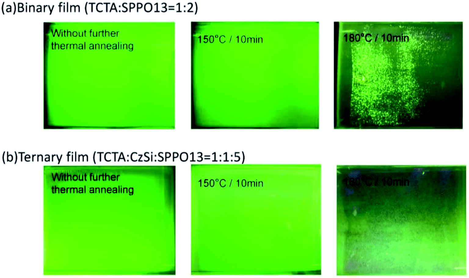
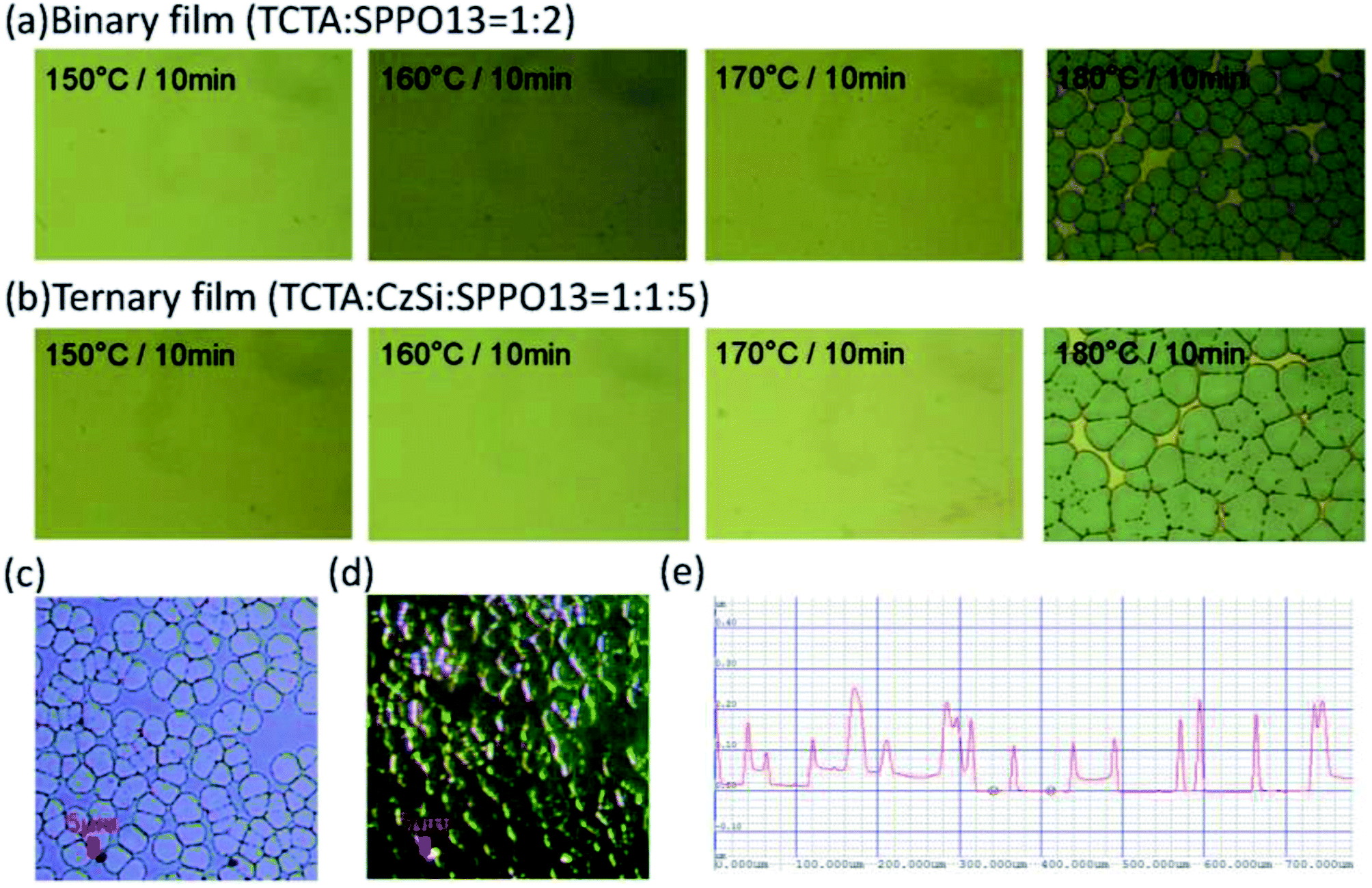
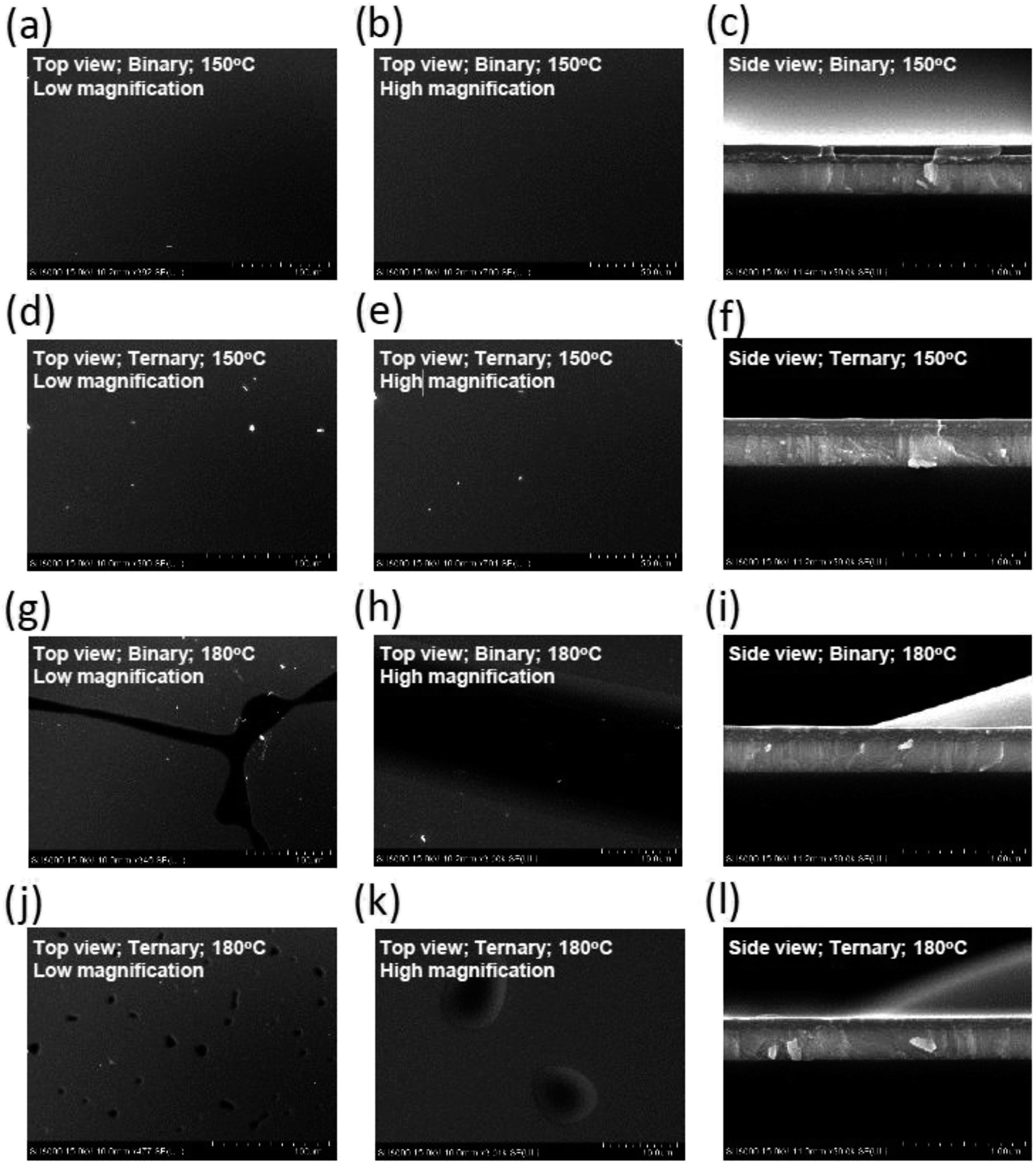
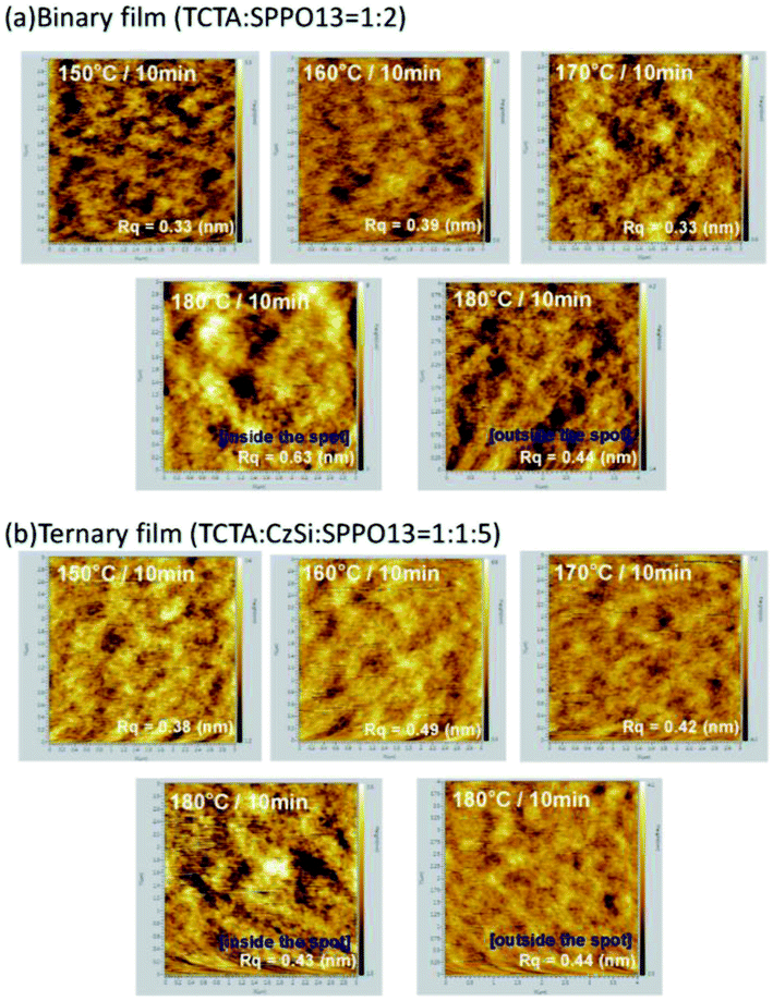
A device structure including the ternary host materials in the EML was applied to the large-active-area green and orange OLED devices (active area: 3 cm × 3.2 cm) to confirm whether the third host played a role in preventing the crystallization of the organic film. At the same time, we optimized the parameters to identify the suitable thickness of the emission layer in the device with the large active area. In Fig. 7(a) and (b), crystallization on the film surface was more obvious in the case of the thicker emission layer, irrespective of whether the device consisted of the binary or ternary host materials. Crystallization was suppressed more prominently in the case of the device with a ternary host than that with a binary host with the same emission layer thickness. This was probably because the ternary composition effectively improved the surface quality of the organic thin film of the OLED during the solution-processed deposition. To get more details on the improved stability of the OLED, photographs, optical microscopy images, scanning electron microscopy (SEM) images and atomic force microscopy (AFM) images of the binary and ternary host films treated with various annealing conditions were investigated. Fig. 8 shows the images of the binary and ternary host films under UV irradiation. The quality of these films annealed at 150 °C is comparable to that of the as-prepared films. However, when the annealing temperature was increased to 180 °C, the brightness of these films was decreased and many bright spots were observed on the binary films. From the optical microscopy images shown in Fig. 9(a) and (b), the film morphology was intact until 180 °C, where many spots can be observed. To get more details on these spots, the bright-field and dark-field optical microscopy images of the binary host film were taken as shown in Fig. 9(c) and (d), respectively. Since the dark-field microscopy images were made by the scattered light, the bright region indicates the area with high roughness, while the dark region indicates the area with a smooth surface. As shown in Fig. 9(c) and (d), the edges of these spots are the places with an abrupt change in thickness. This observation is confirmed by the height profile across these spots as shown in Fig. 9(e). Therefore, these spots are regions with a thinner emissive layer. After high temperature thermal annealing, the materials move and accumulate at the edges of these spots. The morphology of these films was further confirmed by SEM images, as shown in Fig. 10. These images are consistent with the results described above. It is worth mentioning that the emissive layer can be distinguished in the films that were annealed at 150 °C (Fig. 10(c) and (f)), while the emissive materials accumulated into large aggregates on the surface (Fig. 10(i) and (l)) after annealing at 180 °C.
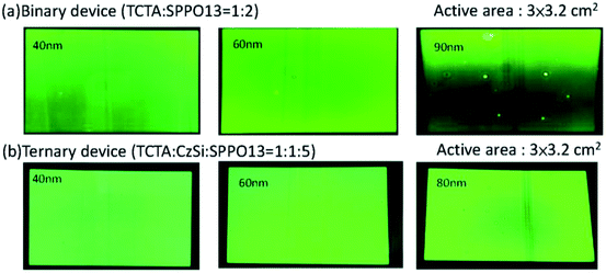 |
| | Fig. 7 Photographs of operating OLED devices with different EML thicknesses (active-area = 3 × 3.2 cm2) (a) binary devices and (b) ternary devices. | |
 |
| | Fig. 8 Photographs of (a) binary films and (b) ternary films under UV irradiation. | |
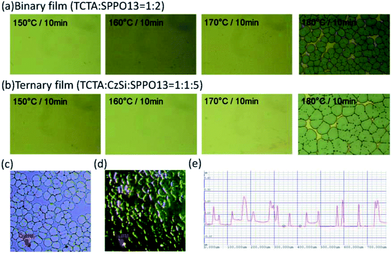 |
| | Fig. 9 Optical microscopy images of (a) binary films and (b) ternary films thermally treated at various temperatures. (c) The bright-field and (d) the dark-field optical microscopy images of the binary host film. (e) The height profile across these spots on the binary host film. | |
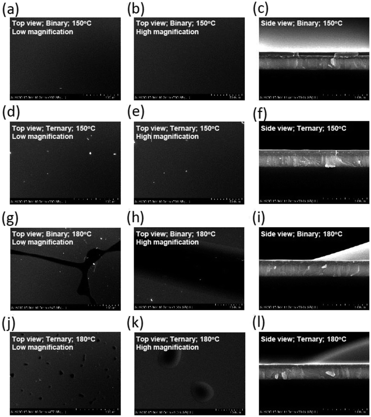 |
| | Fig. 10 (a–c) SEM images of the binary film annealed at 150 °C. (d–f) SEM images of the ternary film annealed at 150 °C. (g–i) SEM images of the binary film annealed at 180 °C. (j–l) SEM images of the ternary film annealed at 180 °C. | |
According to the AFM images shown in Fig. 11, the roughness of the binary films annealed below 170 °C are in the range of 0.3–0.4 nm. This roughness increased to 0.44 nm outside the spot and 0.63 nm inside the spot. On the contrary, all of the roughness values were in the range of 0.4–0.5 nm for the ternary films. It is plausible that the ternary host materials are packed closely in the films, resulting in slightly rougher films and more stable characteristics. Furthermore, according to the literature, the triplet energy (ET) of CzSi (ET = 3.02 eV) is higher than those of SimCP (ET = 2.9 eV) and CzPO2 (ET = 2.82 eV); thus, the addition of CzSi with the higher ET in TCTA (ET = 2.76 eV) and SPPO13 (ET = 2.78 eV) is a better choice in order to confine the excitons in the emissive material.
 |
| | Fig. 11 Atomic force microscopy images of (a) binary films and (b) ternary films thermally treated at various temperatures. | |
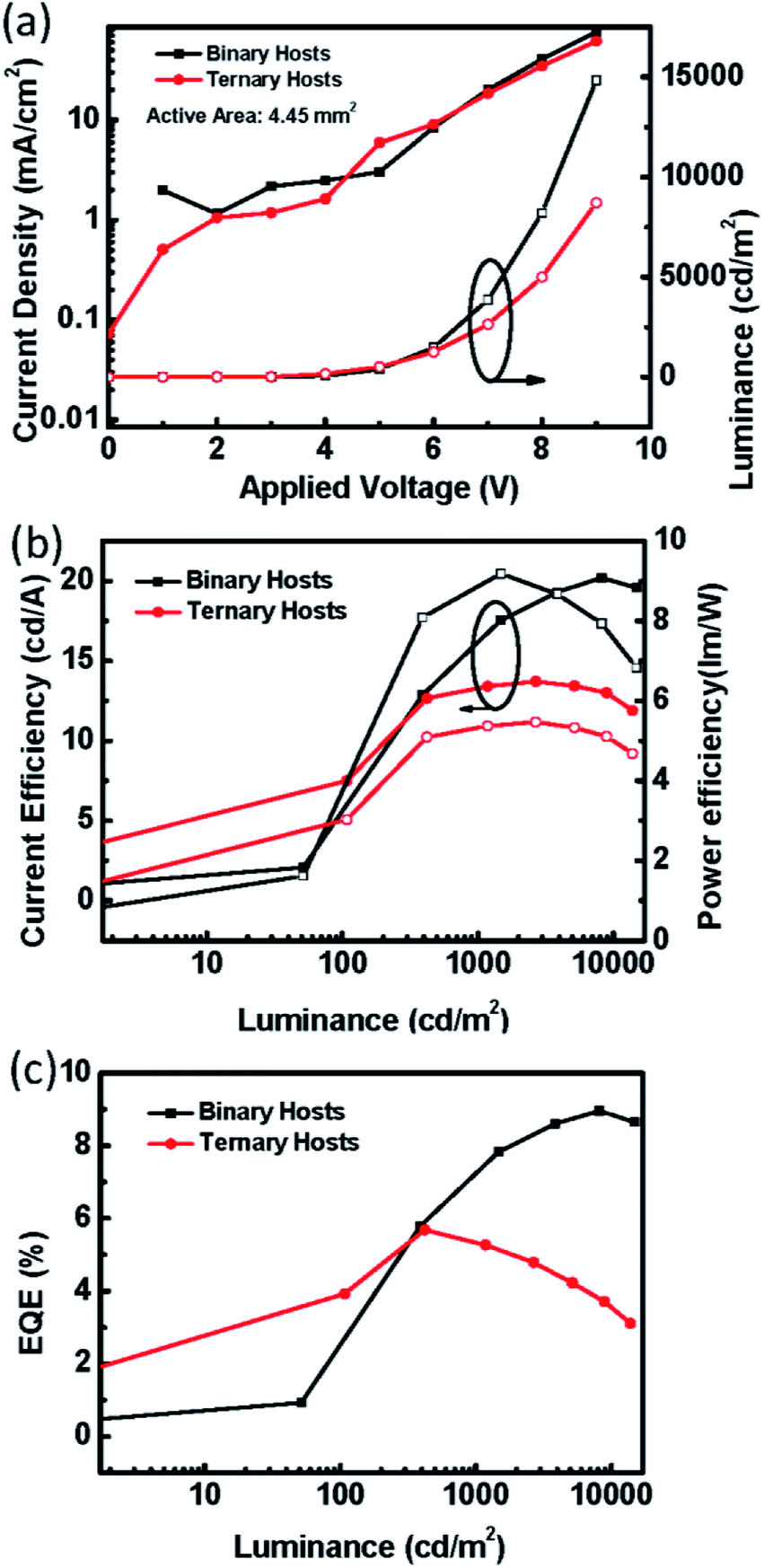
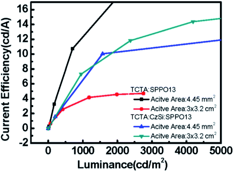
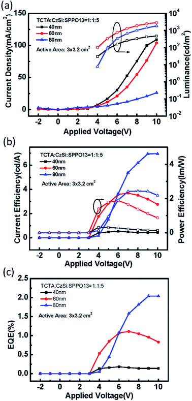
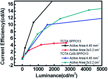
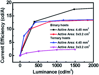
The electrical performances of devices with a ternary host with different emission layer thicknesses are shown in Fig. 12(a–c). The large-active-area ternary device with an 80 nm emission layer showed the best electrical efficiency, with a peak efficiency of 6.95 cd A−1, 2.44 lm W−1, and 2.04%. Although the electrical efficiency of the device with the 80 nm EML was better than that of the device with the 60 nm EML, the results of surface quality followed the opposite trend. The best surface quality was observed for the device with the 60 nm EML, so we applied this thickness to other large-active-area OLED devices (active area = 3 cm × 3.2 cm) in subsequent experiments. Furthermore, we compared four materials as the third host in the emission layer of the large-active-area devices. Fig. 13 shows the performance of the devices with the binary and the ternary hosts at four emission layer compositions. In Fig. 13(b), the applied voltage of the device with a ternary host was obviously lower than that with a binary host when the luminance was 500 cd m−2; this is due to the stable operation of the large-area OLED. The efficiencies of the devices with three host materials in the emission layer were better than that of the device with a binary host. The best result was seen for the device with TCTA, CzSi, and SPPO13, which exhibited a peak efficiency of 15.36 cd A−1, 6.45 lm W−1, and 4.38%. We obtained good results for the device with FATPA as the HOST3. Because of the FATPA molecule with its side-chain, there were no point defects on the EML thin film. The device exhibited good electrical performance. We further compared the relationship between brightness and efficiency; the results are illustrated in Fig. 14. The curves for the small-active-area device and the large-active-area device with ternary host materials overlapped, implying less current leakage in the latter case. It is possible that the molecular stacking composition of the ternary host materials changed the microstructure of the film, thus preventing crystallization in the organic thin film and influencing carrier transport in the device. On the contrary, the device with the binary host material having different active areas showed very different curve characteristics. The point defects on the surface of the organic thin film with the binary host material possibly led to its notable current leakage. We also compared the relationship between brightness and efficiency for large-active-area (active area: 3 cm × 3.2 cm) and small-active-area (active area: 4.45 mm2) orange PhOLEDs. The results showed that the orange PhOLED only requires a binary composition to achieve good film quality. The current efficiency versus luminance curves were shown in Fig. 15.
 |
| | Fig. 12 (a) The current density (solid symbols) and luminance (open symbols) versus applied voltage, (b) the current efficiency (solid symbols) and power efficiency (open symbols) versus applied voltage, (c) the EQE of the ternary green PhOLED devices with different EML thicknesses (active-area = 3 × 3.2 cm2). | |
 |
| | Fig. 13 (a) The current density (solid symbols) and luminance (open symbols) versus applied voltage; (b) luminance versus applied voltage; the current efficiency (solid symbols) and power efficiency (open symbols) versus applied voltage of the device added with (c) CzSi, (d) FATPA, (e) SimCP, (f) and CzPO2; (g) the EQE versus applied voltage; (h) the current efficiency versus luminance of the binary OLED devices and the ternary OLED devices with different third host materials CzSi, SimCP, and CzPO2 (active-area = 3 × 3.2 cm2). (i) The electroluminescence spectra of the binary and ternary devices. | |
 |
| | Fig. 14 The current efficiency versus luminance of binary OLED devices and ternary OLED devices with different active-areas, 3 × 3.2 cm2 and 4.45 mm2. | |
 |
| | Fig. 15 The current efficiency versus luminance of binary orange PhOLED devices and ternary orange PhOLED devices with different active-areas, 3 × 3.2 cm2 and 4.45 mm2. | |
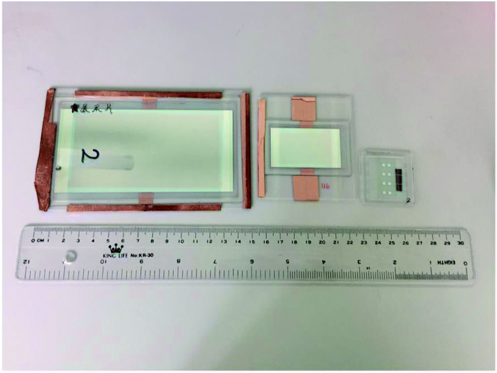
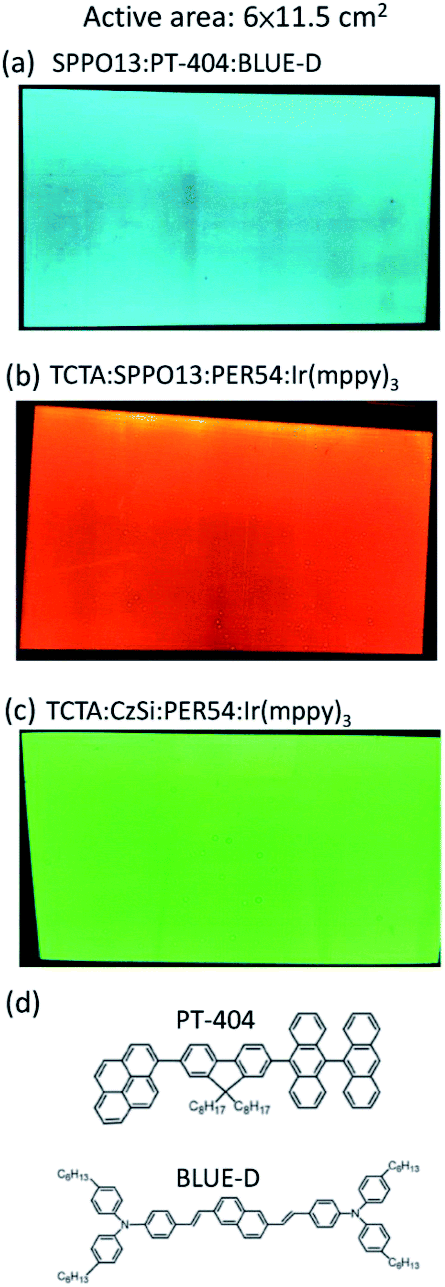
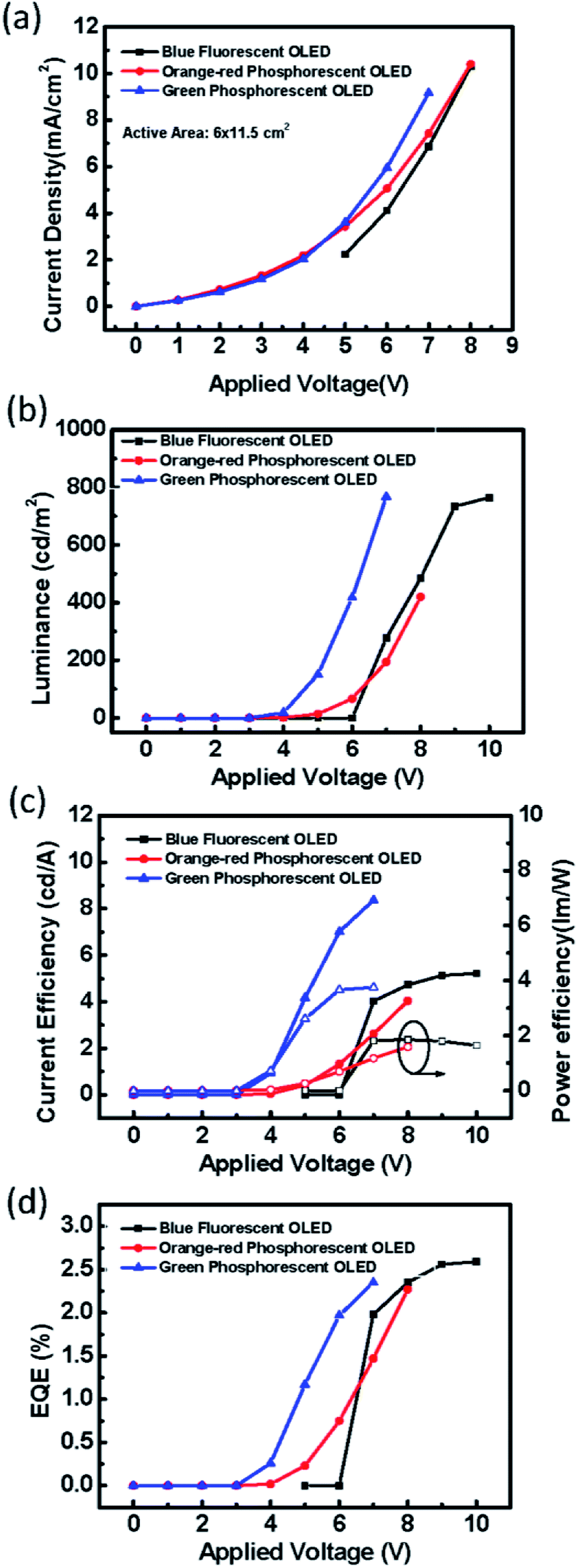
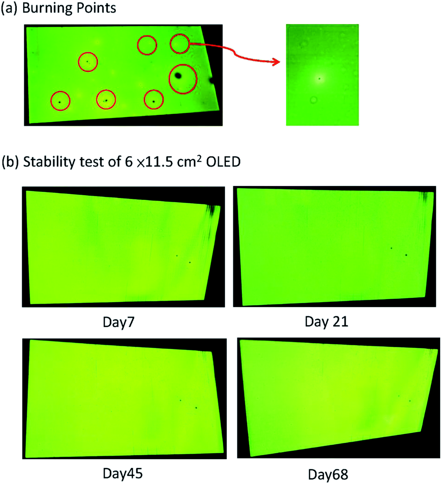
Furthermore, the blade coating process can be applied to fabricate the even larger OLED, with an active area extended to 6 cm × 11.5 cm. There are three substrate sizes of OLED devices in this work, as shown in Fig. 16. For large OLED devices, the single OLED demonstrated outstanding uniformity of luminance. In Fig. 17, there are photographs of operating OLED devices with different colors, including blue, red, and green. In the blue OLED,16 the emission layer is based on a mixed host of 1-(7-(9,90-bianthracen-10-yl)-9,9-dioctyl-9H-fluoren-2-yl)pyrene (PT-404) and the electron-transport material SPPO13, and the blue guest emitter is 4-4′-(1E,1′E)-2,2′-(naphthalene-2,6-diyl)bis(ethane-2,1-diyl)bis(N,N-bis(4-hexyl-phenyl)aniline) (Blue D). For the red OLED, the red emitter PER54 was provided by e-Ray Optoelectronics Technology Co., Ltd. These all-solution-processed OLED devices with large-active-areas had very low operating voltages and did not exhibit any current leakage. The electrical performances of the all-solution-processed OLED devices with large-active-areas are shown in Fig. 18(a–d). After long-time operation, the large OLED develops a burning point if a binary host is used for the green phosphorescent device. On the other hand, not a single burning point developed for the ternary host after a continuous operation lasting more than 1600 hours for the large-active-area OLED (active area = 6 × 11.5 cm2). Fig. 19(a) illustrates some examples of the burning points on an OLED device. Typically, the shapes of the burning points were symmetrical. Fig. 19(b) shows the stability test results for the 6 × 11.5 cm2 OLED. After a continuous operation for up to 1600 hours with an emission area as large as 6 × 11.5 cm2, there were no burning points for the OLED with ternary host materials. We further compared the relationship between brightness and efficiency; the results are illustrated in Fig. 20. In the case of the brightness below 1000 cd m−2, the brightness of the medium sized device (active area: 3 cm × 3.2 cm) increases quickly. In Fig. 20(b), we did not get the measured efficiency points of the medium sized device between 0 cd m−2 and 1000 cd m−2. The curves for the small-active-area device, medium-active-area device and the large-active-area device with ternary host materials overlapped, implying that less current leakage occurred in the latter case. The composition of the ternary host materials was very effective for reducing the operating voltage of the OLED devices and improving the quality of the emission layer to reduce the current leakage.
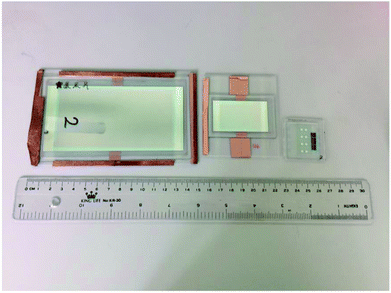 |
| | Fig. 16 A photograph of OLED devices of three different sizes in our laboratory, with substrate: 9 × 15 cm2, 7 × 8 cm2 and 4 × 4 cm2. | |
 |
| | Fig. 17 Photographs of large-active-area OLED devices with different colors (active-area = 6 × 11.5 cm2). (a) Blue fluorescent OLED, (b) red phosphorescent OLED and (c) green fluorescent OLED. (d) Molecular structures of the organic materials, PT-404 and BLUE-D, used in the blue OLED. | |
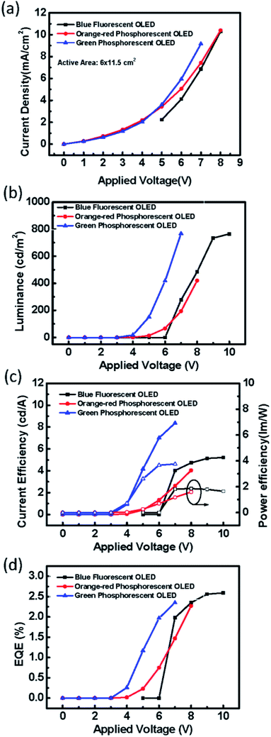 |
| | Fig. 18 (a) The current density versus applied voltage, (b) luminance versus applied voltage, (c) the current efficiency (solid symbols) and power efficiency (open symbols) versus applied voltage, and (d) the EQE of large-active-area OLED devices with different colors (active-area = 6 × 11.5 cm2). | |
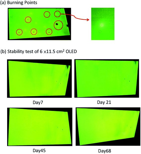 |
| | Fig. 19 (a) Burning points of OLED. (b) Stability test results of 6 × 11.5 cm2 OLED with no burning point defects appearing after operating for over 1600 h (68 days). | |
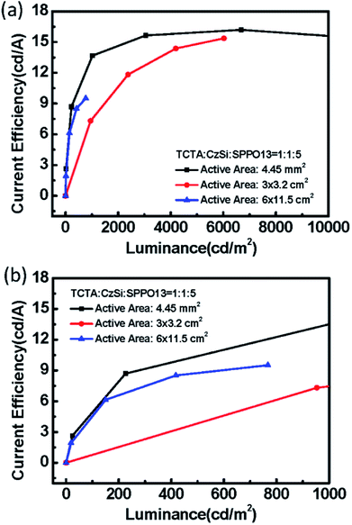 |
| | Fig. 20 (a) The current efficiency versus luminance, (b) the current efficiency versus luminance (0 to 1000 cd m−2) of ternary green PhOLED devices with different active-areas of 6 × 11.5 cm2, 3 × 3.2 cm2 and 4.45 mm2. | |
Conclusions
One of the greatest challenges for solution-processed OLEDs in lighting applications is the point defects that cause electrical current leakage or even short circuits. The wet process is prone to defects due to the formation of aggregates or micro-crystals in the organic molecules. Local film cracks beneath the cathode may cause current concentration and local over-heating after long-time operations, i.e., a burning point. In this work, we demonstrated that all of the current-leakage defects can be avoided by two approaches. One is the careful control of the coating conditions in the blade coating processes. Another is the use of a ternary host for the phosphorescent emission layer. The ternary host may interrupt the tendency for micro-crystallization to occur and significantly reduces the operation voltage. The operation voltage is 4 V at 100 cd m−2. For a large emission area of 6 × 11.5 cm2, the single OLED without pixels develops no burning point after 1600 hours of continuous operation. Such stability makes it possible for the initial commercial application of all-solution processed OLED lighting with low cost, easy single-diode driving, and beautiful natural colors at a comfortable brightness.
Authorship
Y. F. Chang, H. F. Meng and Y. C. Chao conceived the study and wrote the manuscript. S. Y. Liao, H. T. Su, Y. H. Hsiao, Y. F. Chang, C. W. Chang, M. C. Niu and C. Yen conducted the experiments. H. F. Meng, Y. C. Chao, C. Y. Chang, H. W. Zan and S. F. Horng contributed to interpretation of the results and improvement of the manuscript.
Conflicts of interest
There are no conflicts to declare.
Acknowledgements
This work was supported by the National Science Council of Taiwan under Contract No. NSC 106-2622-M-009-005-CC2. The authors thank the Dept. of Organic Light Emitting Materials Device Research, Industrial Technology Research Institute for providing the organic material PR-02.
Notes and references
- L. Duan, L. Hou, T. W. Lee, J. Qiao, D. Zhang, G. Dong, L. Wang and Y. Qiu, J. Mater. Chem., 2010, 20, 6392 RSC.
- B. Wang, Z. K. Wang, J. Liang, M. Li, Y. Hu and L. S. Liao, J. Mater. Chem. C, 2017, 5, 10721 RSC.
- M. Cai, T. Xiao, E. Hellerich, Y. Chen, R. Shinar and J. Shinar, Adv. Mater., 2011, 23, 3590 CrossRef CAS PubMed.
- J. Y. Seok and M. Yang, Adv. Mater. Technol., 2016, 1, 1600029 CrossRef.
- C. Y. Chen, H. W. Chang, Y. F. Chang, B. J. Chang and Y. S. Lin, et al., J. Appl. Phys., 2011, 110, 094501 CrossRef.
- H. C. Yeh, H. F. Meng, H. W. Lin, T. C. Chao, M. R. Tseng and H. W. Zan, Org. Electron., 2012, 13, 914 CrossRef CAS.
- Y. F. Chang, Y. C. Chiu, H. C. Yeh, H. W. Chang, C. Y. Chen, H. F. Meng, H. W. Lin, H. L. Huang, T. C. Chao, M. R. Tseng, H. W. Zan and S. F. Horng, Org. Electron., 2012, 13, 2149 CrossRef CAS.
- Y. F. Chang, H. F. Meng, G. L. Fan, K. T. Wong, H. W. Zan, H. W. Lin, H. L. Huang and S. F. Horng, Org. Electron., 2016, 29, 99 CrossRef CAS.
- Y. F. Chang, C. H. Yu, S. C. Yang, I. H. Hong, S. C. Jiang, H. F. Meng, H. L. Huang, H. W. Zan and S. F. Horng, Org. Electron., 2017, 42, 75 CrossRef CAS.
- L. S. Yang, H. F. Meng, Y. F. Chang, C. H. Lien, H. W. Zan, S. F. Horng, L. Duan, Y. Qiu and C. W. Luo, Org. Electron., 2017, 451, 6 CrossRef.
- T. H. Han, M. R. Choi, C. W. Jeon, Y. H. Kim, S. K. Kwon and T. W. Lee, Sci. Adv., 2016, 2, e1601428 CrossRef PubMed.
- L. Duan, D. Zhang, K. Wu, X. Huang, L. Wang and Y. Qiu, Adv. Funct. Mater., 2011, 21, 3540 CrossRef CAS.
- Q. Fu, J. Chen, C. Shi and D. Ma, ACS Appl. Mater. Interfaces, 2012, 4, 6579 CrossRef CAS PubMed.
- W. Li, J. Li, F. Wang, Z. Gao and S. Zhang, ACS Appl. Mater. Interfaces, 2015, 7, 26206 CrossRef CAS PubMed.
- C. Han, Z. Zhang, H. Xu, J. Li, G. Xie, R. Chen, Y. Zhao and W. Huang, Angew. Chem., Int. Ed., 2012, 51, 10104 CrossRef CAS PubMed.
- L. S. Yang, H. F. Meng, Y. F. Chang, C. H. Lien, H. W. Zan, S. F. Horng, L. Duan, Y. Qiu and C. W. Luo, Org. Electron., 2017, 51, 6–15 CrossRef CAS.
Footnote |
| † Electronic supplementary information (ESI) available. See DOI: 10.1039/c8ra10363a |
|
| This journal is © The Royal Society of Chemistry 2019 |
Click here to see how this site uses Cookies. View our privacy policy here. 
 Open Access Article
 This Open Access Article is licensed under a Creative Commons Attribution-Non Commercial 3.0 Unported Licence
 *d,
Chih-Yu Change,
Hsiao-Wen Zan
*d,
Chih-Yu Change,
Hsiao-Wen Zan