
 Open Access Article
 This Open Access Article is licensed under a Creative Commons Attribution-Non Commercial 3.0 Unported Licence
Enhanced thermoelectric properties in N-type Mg2Si0.4−xSn0.6Sbx synthesized by alkaline earth metal reduction
Jin Chenab,
Wenhua Xueb,
Shan Lib,
Gengxin Zhanga,
Gemei Cai *a and
Huaizhou Zhao*b
*a and
Huaizhou Zhao*b
aSchool of Materials Science and Engineering, Central South University, Changsha, China. E-mail: caigemei@csu.edu.cn; Fax: +86-731-88877732; Tel: +86-731-88877732
bInstitute of Physics, Chinese Academy of Science, Beijing, China. E-mail: Hzhao@iphy.ac.cn
First published on 30th January 2019
Abstract
Mg2Si1−xSnx-based compounds have been recognized as promising thermoelectric materials owing to their high figure-of-merit ZTs, abundance of raw constituent elements and nontoxicity. However, further improvement in the thermoelectric performance in this type of material is still constrained by the high thermal conductivity. In this work, we prepared a series of representative Mg2Si0.4−xSn0.6Sbx (x = 0, 0.0075, 0.008, 0.009, 0.01, 0.011) samples via the alkaline earth metal reduction method through a combination of ball milling and spark plasma sintering (SPS) processes. The samples featured many dislocations at the grain boundaries and plenty of nanoscale-coherent Mg2Si–Mg2Sn spinodal phases; both of which can effectively scatter heat-carrying phonons and have nearly no impact on the carrier transport. Meanwhile, Sb-doping can efficiently optimize the carrier concentration and significantly suppress the bipolar effects. As a result, a maximal ZT of 1.42 at 723 K and engineering (ZT)eng of 0.7 are achieved at the optimal Sb-doping level of x = 0.01. This result indicates that the alkaline earth metal reduction method could be an effective route to engineer phonon transport and improve the thermoelectric performance in Mg2Si1−xSnx-based materials.
Introduction
Thermoelectric materials can directly convert waste heat into electricity, which will improve the ultimate efficiency of thermal energy utilization. Taking the reality of severely increased waste heat energy dissipation into account, thermoelectric materials contribute to the development of green and sustainable energy for society.1,2 The performance of thermoelectric materials is usually evaluated by a dimensionless figure-of-merit, ZT = S2T/ρK, where S, ρ, K and T are the Seebeck coefficient, electrical resistivity, thermal conductivity and absolute temperature, respectively. On the whole, thermoelectric transport consists of two correlative processes: the electrical and thermal transport processes, where electrical transport is generally quantified by the thermoelectric power factor (PF = S2/ρ), in which S and ρ (ρ = 1/neμ) are counter-related through the carrier concentration n under a single parabolic band (SPB) model for acoustic phonon dominated systems:3
 | (1) |
Furthermore, the thermal transport process is mostly carried out by acoustic phonons and charge carriers, which are referred to as the phonon part (Kl) and the charge carrier part (Ke). Because Ke and ρ are further coupled through the Wiedemann–Franz law, we can say that Ke = LT/ρ, where L is known as the Lorenz number. Thus, the enhancement of ZT values through the independent tunings of thermoelectric parameters S, ρ and K is challenging. However, ideal thermoelectric materials require a synergistically high power factor and low thermal conductivity, and measures should be taken to achieve this goal. Instinctively the fundamental approach to increase electrical transport is to modulate carrier concentrations;4–6 other approaches include delicate tuning of the band effective mass and mobility through band engineering.7–12 Another strategy is to decrease the relatively independent parameter, lattice thermal conductivity Kl, through increased phonon scatterings by multiple crystal defects, such as point defects, grain boundaries, nanoscale precipitations, dislocations, or by taking advantage of the intrinsically anharmonic phonons for low lattice thermal conductivity, etc.13–18
Mg2Si-based compounds are treated as promising thermoelectric materials because of their nontoxicity and low cost and because of the abundance of the constituent elements. However, the low power factor and high lattice thermal conductivity in pristine Mg2Si materials inhibit the improvement of thermoelectric performance. Liu et al. found that the Mg2Si–Mg2Sn solid solutions favor convergence of the conduction band, leading to an increase of the density-of-states effective mass, and therefore Seebeck coefficient and ZT.19 Zhang et al. also found that Sb-doping on the Si site can optimize the carrier concentration and effectively tune the band structures, leading to an increased power factor.20 Furthermore, Tang and Jang et al. reported that the Mg2Si0.4Sn0.6 solid solution doped with Sb could form a coherent interface in nanostructures, thus effectively scattering mid-frequency phonons while having little influence on carrier transport.21,22
The alkaline earth metal reduction method, which was first described in our previous work in half-Heusler materials including both n-type Hf0.025Zr0.075NiSn0.97Sb0.03 and p-type Nb0.8Ti0.2FeSb, proves to be effective in inhibiting the thermal transport process and has little influence on electrical transport.23 Since the high thermal conductivity also constrains the thermoelectric performance of Mg2Si1−xSnx-based materials, we introduce this novel method to synthesize high purity Mg2Si0.4Sn0.6 bulk samples, as shown in the following chemical reaction equation:
| 2.6Mg + (0.4 − x)Si + 0.6SnCl2 + xSb = Mg2Si0.4−xSn0.6Sbx + 0.6MgCl2 |
Notably, chlorides and metal substances were used as raw materials to perform ball milling and then the spark plasma sintering (SPS) process. Primarily, the Sb-dopant optimized the carrier concentration and effectively suppressed the bipolar effects in thermal conductivity, raising the PF to a high level. Meanwhile, the dislocations at the grain boundaries and the nanoscale-coherent Mg2Si–Mg2Sn spinodal phases in the matrix strongly scattered the transport phonons, leading to reduced lattice thermal conductivity, but only with a trivial impact on electrical transport. As a result, the thermoelectric performance of Mg2Si0.4−xSn0.6Sbx in the whole temperature range was enhanced, with a maximum ZT of 1.42 at 723 K at the doping level of x = 0.01.
It is noted that the thermoelectric performance here is obviously higher than that of the samples synthesized through traditional methods,20,22 even though the thermoelectric performance is a little lower than the optimal performance in the report with a maximum ZT of 1.50 at 716 K.24 However, the alkaline earth metal reduction method is less time-consuming and simpler than the synthetic process that combines the molten-salt sealing method with pulsed electric sintering densification.24 This result proved that the alkaline earth metal reduction method with a combination of ball milling and the SPS process is a dominant and simple method to enhance the thermoelectric performance of Mg2Si1−xSnx-based materials.
Experiments
Synthetic procedures
The Mg2Si0.4Sn0.6 and five Sb-doped Mg2Si0.4Sn0.6 bulk samples were synthesized through a mechanochemical reaction and SPS process. The raw materials including tin(II) chloride anhydrous (SnCl2, 98%, powders), magnesium (Mg, 99.8%, turnings), silicon (Si, 99%, powders) and antimony (Sb, 99.999%, pieces) were weighed according to the stoichiometry of Mg2.7Si0.4−xSn0.6Sbx (x = 0, 0.0075, 0.008, 0.009, 0.01, 0.011) in an Ar-filled glove box. The excess Mg was used not only to reduce Sn from SnCl2, but also to compensate for evaporation of Mg during the reaction process. All 5 g of materials were then transferred into the stainless ball milling jar to undergo a 6 h high-energy ball milling process (SPEX Sample Prep 800 Mixer/Mill), at between 1425 and 1725 revolutions per minute (rpm). Finally, the obtained precursor powder was loaded into a graphite die (diameter, 12.7 mm) and sintered by SPS at 1023 K for 15 min under a pressure of 50 MPa.Phase and morphologies analysis
The phase analysis was performed by X-ray diffraction (XRD; Xpert Pro PANalytical XRD) using Cu-Kα radiation (λ = 1.5418 Å) and operating under 40 kV and 40 mA in a 2θ range between 20° and 80° in the air. The microstructures of the samples were characterized by scanning electron microscopy (SEM; XL30S-FFG) and transmission electron microscopy (TEM; JEM-2100 Plus). The accelerating voltages for the SEM and TEM were 15 kV and 200 kV, respectively.Thermoelectric properties analysis
The temperature-dependent electrical resistivity and Seebeck coefficient were measured using commercial equipment (LSR-3, Linseis) protected by high purity helium. The temperature-dependent thermal diffusivity (D) was measured by a laser flash system (LFA-1000, Linseis) at the atmosphere of high purity helium, and the total conductivity was calculated by Ktot = DCpd, where Cp is the specific heat capacity estimated by Dulong–Petit law Cp = 3NR, N and R are the gas constant and the ratio of atomic number to molar mass, respectively, and d is the density measured by Archimedes drainage method. The room-temperature Hall analysis, including carrier concentration (n) and carrier mobility (μ), was carried out using the van der Pauw method under a magnetic field of 0.5 T.Results and discussion
Structures and morphologies analysis
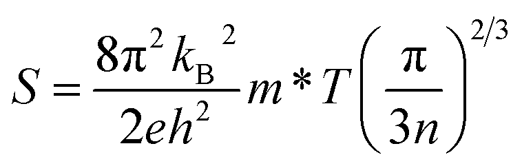
Six typical samples were synthesized through this new method, and were characterized by XRD as shown in Fig. 1(a). It can be seen that a single-phase pattern is obtained. The main diffraction peaks of the patterns can be indexed to an anti-fluorite-type structure (Fm3m), and the strongest two peak positions of the samples are located between the peaks of pure Mg2Si and Mg2Sn, indicating the formation of Mg2Si–Mg2Sn solid solution and the successful doping of Sb, which is consistent with previous results.20,21,25 As the inset of Fig. 1(b) shows, the crystal structure of Mg2Si0.4Sn0.6 includes two types of lattice site, in which 16c is occupied by Mg while Si and Sn co-occupied 8b.26 When Sb partly replaces Si in the Mg2Si0.4Sn0.6 matrix, the crystal lattice expands because the atomic radius of Sb is larger than that of Si. The lattice parameters of the six samples are calculated and displayed as a function of the antimony doping level in Fig. 1(b), which is consistent with previous results.20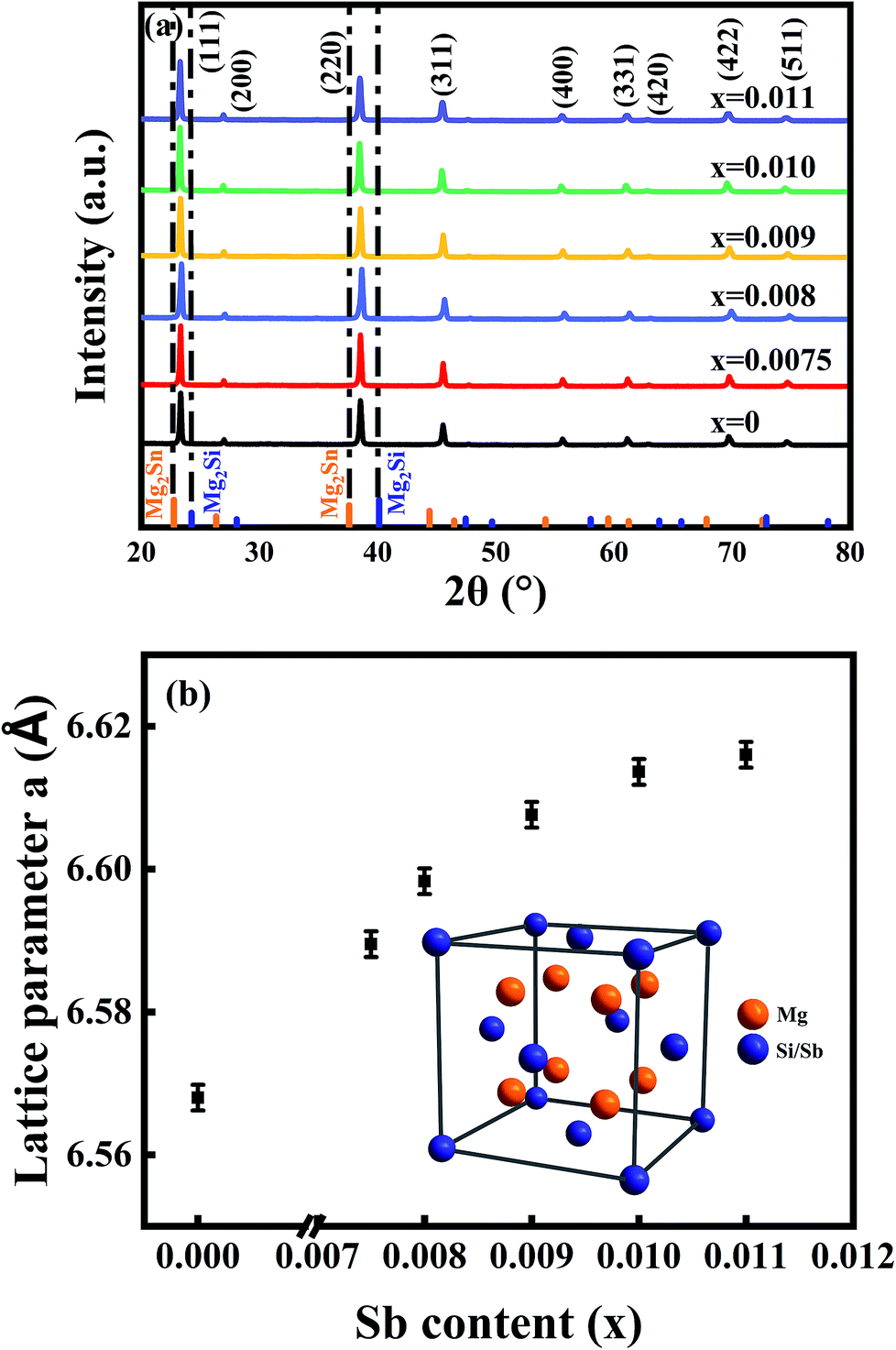 | ||
| Fig. 1 (a) XRD patterns for all samples and (b) antimony doping dependence of lattice parameters for a series of Sb-doped Mg2Si1−xSn0.6Sbx (x = 0, 0.0075, 0.008, 0.009, 0.01, 0.011) compounds. The inset image shows the crystal structure of Mg2Si/Sn. | ||
Fig. 2(a) presents the morphology and structure of the fractured surface of the Mg2Si0.39Sn0.6Sb0.01 sample. There are clearly pores along the surface, which can be ascribed to the extrusion of magnesium chloride. However, the density of these samples is still 93–95% of the theoretical density. The grain sizes are around 5–10 μm, and clear edges can be observed at the boundaries, exhibiting good crystallization by using this new synthetic method. In Fig. 2(b), the high-magnification SEM image shows that there are no clear inclusions or precipitations between the crystalline boundaries and in the inner grains, indicating the formation of a continuous Mg2Si–Mg2Sn solid solution.22
 | ||
| Fig. 2 SEM images of (a) low-magnification and (b) high-magnification of the optimal composite Mg2Si0.39Sn0.6Sb0.01. | ||
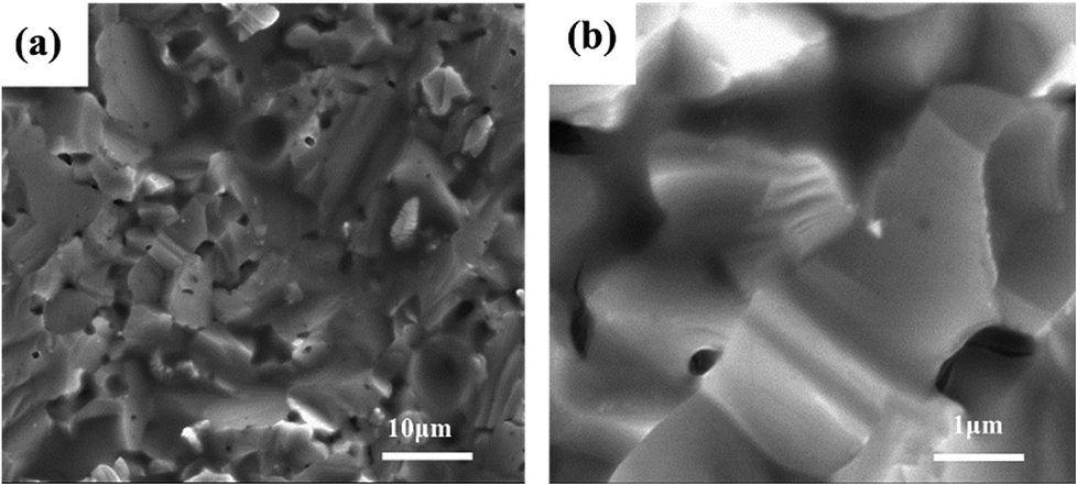
Fig. 3 shows the TEM images of Mg2Si0.39Sn0.6Sb0.01. Fig. 3(a) represents the TEM image of the grain boundaries. To identify structural information among the grain boundaries with greater clarity, a magnified TEM image was obtained, as shown in Fig. 3(b). The dislocations at the grain boundaries can clearly be seen, which would scatter the phonons and decrease the thermal conductivity. Furthermore, the dislocations are mainly located at the boundaries, which would be beneficial for the decoupling of electrical transport and phonon transport inside the grains. A similar result can be seen in half-Heusler systems synthesized by the same route.23
 | ||
| Fig. 3 (a) TEM image of the grain boundary. (b) TEM image of the dislocations in the matrix. (c) TEM image of the matrix. (d) Selected area electron diffraction image of the matrix. (e) High resolution TEM image of the selected (inset shows the fast Fourier transform pattern of the matrix). (f) High resolution TEM image of coherent matrix with the optimal doping level x = 0.01. | ||
Furthermore, Fig. 3(c) and (d) show the TEM image and the corresponding selected area electron diffraction (SAED) image of the matrix, respectively. According to the SAED pattern, the matrix conforms with the zone axis [0 1 1] of the Fm3m structure. The Fast Fourier Transform pattern of the matrix in Fig. 3(e) shows that there are two sets of diffraction pattern, which indicates that the matrix is composed of different structures. The red points are assigned to the zone axis [0 1 1] of Mg2Sn, and the yellow points are assigned to the zone axis [![[2 with combining macron]](https://www.rsc.org/images/entities/char_0032_0304.gif) 1 5] of Mg2Si. In order to obtain more information about the matrix, a high resolution TEM image of the matrix is shown in Fig. 3(f). From the high resolution TEM image, it is clear that the matrix is composed of many spinodal phases, consistent with the result of fast Fourier transform patterns. Furthermore, the inter-planar distances of the planes in the selected areas correspond to (2 0 0) and (
1 5] of Mg2Si. In order to obtain more information about the matrix, a high resolution TEM image of the matrix is shown in Fig. 3(f). From the high resolution TEM image, it is clear that the matrix is composed of many spinodal phases, consistent with the result of fast Fourier transform patterns. Furthermore, the inter-planar distances of the planes in the selected areas correspond to (2 0 0) and (![[4 with combining macron]](https://www.rsc.org/images/entities/char_0034_0304.gif) 2 ) of Mg2Sn and Mg2Si, respectively. It is generally believed that the coherent spinodal structure in the matrix would not have a significant impact on the electrical transports. However, the spinodal structures might result in strong phonon scattering owing to mass fluctuation and lattice dislocations. Thus, the coherent spinodal structures would facilitate the thermoelectric transport in these materials by decoupling the thermal and charge carrier transports, leading to enhanced ZT.
2 ) of Mg2Sn and Mg2Si, respectively. It is generally believed that the coherent spinodal structure in the matrix would not have a significant impact on the electrical transports. However, the spinodal structures might result in strong phonon scattering owing to mass fluctuation and lattice dislocations. Thus, the coherent spinodal structures would facilitate the thermoelectric transport in these materials by decoupling the thermal and charge carrier transports, leading to enhanced ZT.
Thermal conductivity analysis
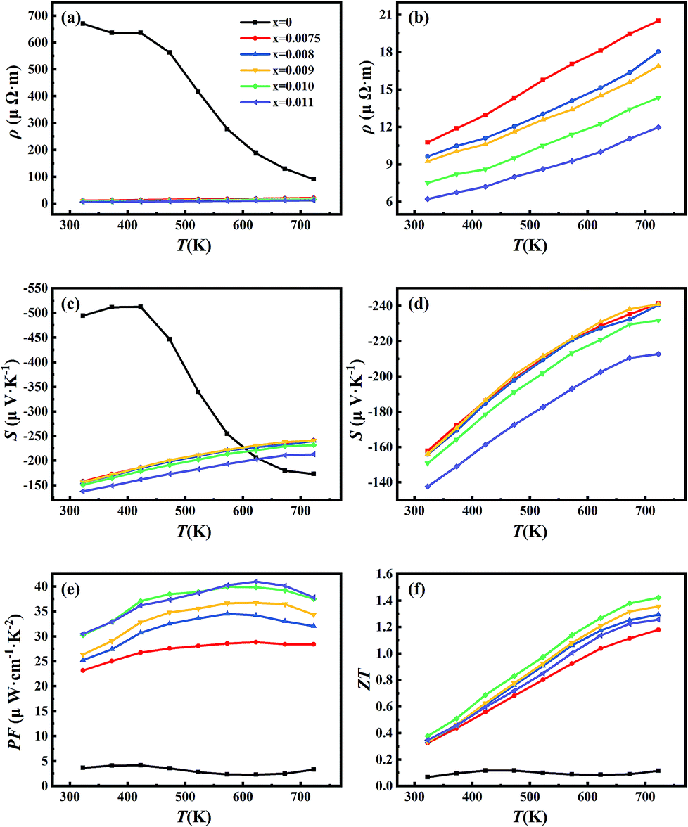
Fig. 4(a) shows the temperature dependence of total thermal conductivity (Ktot) for all samples. As the doping level increases, the total thermal conductivity increases; while the total thermal conductivity decreases as the temperature increases. As shown in Fig. 4(a), the thermal conductivity of the undoped sample reaches a minimum and starts to increase at 423 K, indicating the occurrence of a bipolar effect. The bipolar thermal conductivity has a contribution from the minority of carriers in the materials, which cannot be ignored when the temperature is sufficiently high.27 Thus, there would be a significant increase of thermal conductivity in the undoped sample. However, as for the Sb-doped samples, the thermal conductivity was continuously decreasing, and the bipolar effect was substantially suppressed.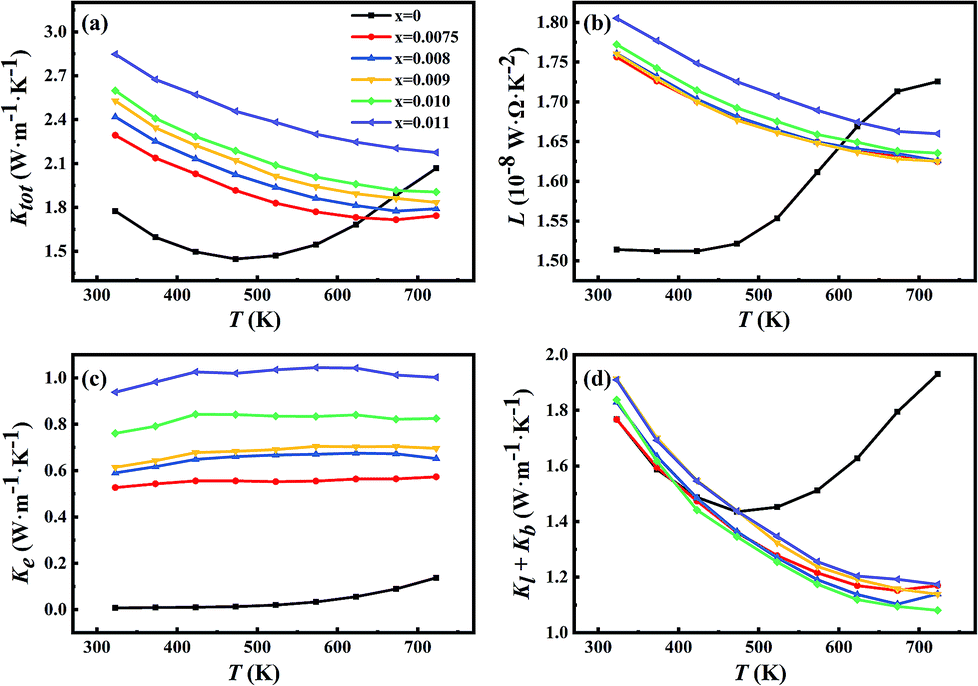 | ||
| Fig. 4 Temperature dependence of (a) total thermal conductivity, (b) Lorenz number, (c) carrier thermal conductivity and (d) lattice and bipolar conductivity for all samples. | ||
The total thermal conductivity can be divided into three parts: lattice thermal conductivity (Kl), carrier thermal conductivity (Ke) and bipolar thermal conductivity (Kb). The carrier thermal conductivity is calculated through the Wiedemann–Franz law as mentioned above, in which the Lorenz number can be estimated according to SPB model as follows:28
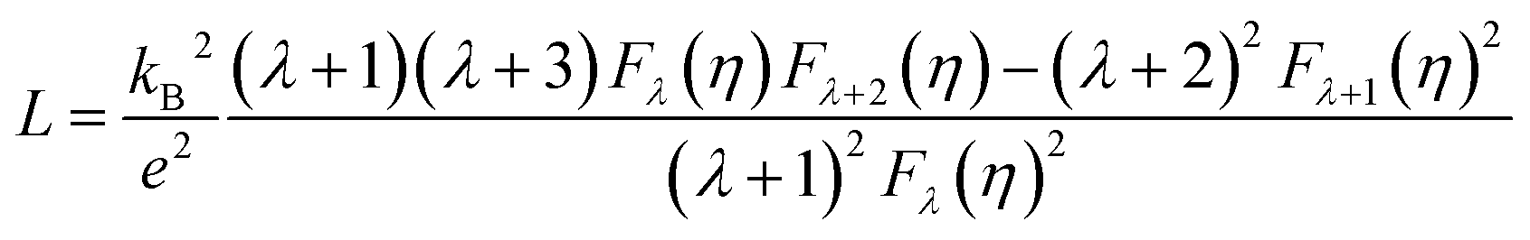 | (2) |
 | (3) |
The Lorenz number L and electrical thermal conductivity Ke are calculated and shown in Fig. 4(b) and (c), respectively. Fig. 4(d) shows the sum of the lattice thermal conductivities and bipolar thermal conductivities of all samples. As for the Sb-doped samples, the lattice thermal conductivity decreases as the Sb-doping level increases, which can be explained by the enhancement of scattering effects due to dislocations and the nanoscale spinodal structure, as shown in Fig. 3, and it approximately follows a T−1 law that indicates the Umklapp process dominated phonon transport.31 However, as for the undoped sample, the sudden increase of Kl + Kb from 423 K indicates the occurrence of a bipolar effect and the minority carrier plays a significant role in the thermal transport.4
Electrical transport analysis
Room-temperature Hall measurements were performed, as shown in Fig. 5(a). The carrier concentration increases with the Sb-doping level, which is ascribed to the donor effect by Sb5+ atom substitution on Si4+ sites in the host matrix. At the same time, the carrier mobility decreases slightly, which is due to the scattering of the carrier by point defects and other nanoscale structures.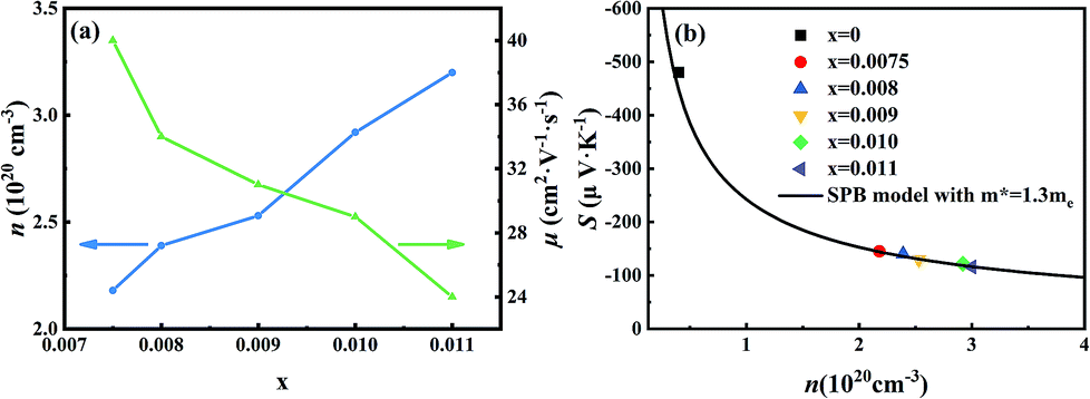 | ||
| Fig. 5 (a) Room-temperature Hall carrier concentration and carrier mobility of a series of Sb-doped Mg2Si1−xSn0.6Sbx (x = 0.0075, 0.008, 0.009, 0.01, 0.011) compounds. (b) Pisarenko relation plot (black solid line) based on the assumption of a SPB mode with m* = 1.3me at room temperature compared with the scatter plot of the experimental data of all samples. | ||
The plot of the room-temperature Seebeck coefficient as a function of carrier concentration is shown in Fig. 5(b), compared with the Pisarenko line under the assumption of a simple parabolic band model:28
 | (4) |
 | (5) |
 | (6) |
As Fig. 5(b) shows, the experimental data match well with the Pisarenko curve at room temperature, revealing that the SPB model still appropriately describes the electronic transport of those Mg2Si0.4Sn0.6-based samples at room temperature.
Fig. 6 shows the temperature-dependent electrical resistivity, Seebeck coefficient, power factor and ZT for all samples and related ref. 20 and 22. Among them, Fig. 6(a) indicates that the electrical resistivity decreases sharply with the Sb-doping in Mg2Si0.4Sn0.6. Fig. 6(b) represents the magnified electrical resistivity of five Sb-doped samples, which clearly shows that the resistivity decreases with increases in Sb-doping level and increase of carrier concentration, as shown in the room-temperature Hall measurements. Furthermore, the electrical resistivity of five Sb-doped samples increases with temperature, indicating the characteristics of heavily doped semiconductor behavior. Clearly, it is proven that by using the new simple synthetic route, Sb can be effectively doped into Mg2Si0.4Sn0.6 and so increase the carrier concentration, leading to transformation from non-generated semiconductor behaviors to generated semiconductor behaviors in Mg2Si0.4Sn0.6.4
 | ||
| Fig. 6 Temperature dependence of (a) electrical resistivity, (c) Seebeck coefficient, (e) power factor and (f) ZT for all samples. (b) and (d) are the magnified electrical resistivity and Seebeck coefficient for all Sb-doped samples, respectively. | ||
In addition, the resistivity of the undoped sample decreases from 423 K, ascribed to the intrinsic excitation and the contribution of minority carrier to the carrier transport.32 However, no obvious decrease in the electrical resistivity of Sb-doped samples in comparison with the undoped sample was observed, indicating that adding Sb could significantly increase the density of the major carriers. Fig. 6(c) and (d) show that the Seebeck coefficient decreases as the Sb-doping level increases, which originates from the increase of carrier concentration according to eqn (1). As for the undoped sample, there is a clear decrease from 423 K, which is due to the occurrence of bipolar effects. Because of the opposite electric charge between minority and majority carriers, the Seebeck coefficient decreases clearly when the bipolar effect occurs. Further, the sudden decrease of Seebeck coefficient is consistent with that in electrical resistivity and the increase of thermal conductivity.27 Fig. 6(e) presents the temperature dependence of the power factor for all samples. It indicates that PF increases with doping level. When the doping level reaches above 0.01, the PF hits the maximum value from the whole temperature range. The increase of PF with Sb-doping level could be explained by two reasons. On one hand, the optimization of carrier concentration through Sb-doping approaches the maximal PF. Furthermore, the optimized carrier concentration by adding Sb effectively suppress the bipolar effects. Overall, the dimensionless figure-of-merit for all samples is calculated and shown in Fig. 6(f). It is shown that with increasing Sb-doping level, the ZT increases and reaches a maximum of 1.42 at 723 K at a doping level x = 0.01. The high ZT in the work originates for two reasons: on one hand, Sb-doping optimizes the carrier concentration and suppresses the bipolar effects, leading to optimized thermoelectric power factor. On the other hand, the new synthetic approach allows the formation of a number of dislocations at the grain boundaries and plenty of coherent spinodal structures in the matrix of the Mg2Si0.4Sn0.6 samples, which would effectively scatter the heat-carrying phonons, while having little impact on the charge carrier transport. Thus, the decoupling of electrical and phonon transports is realized in Sb-doped Mg2Si0.4−xSn0.6Sbx with enhanced thermoelectric performance.
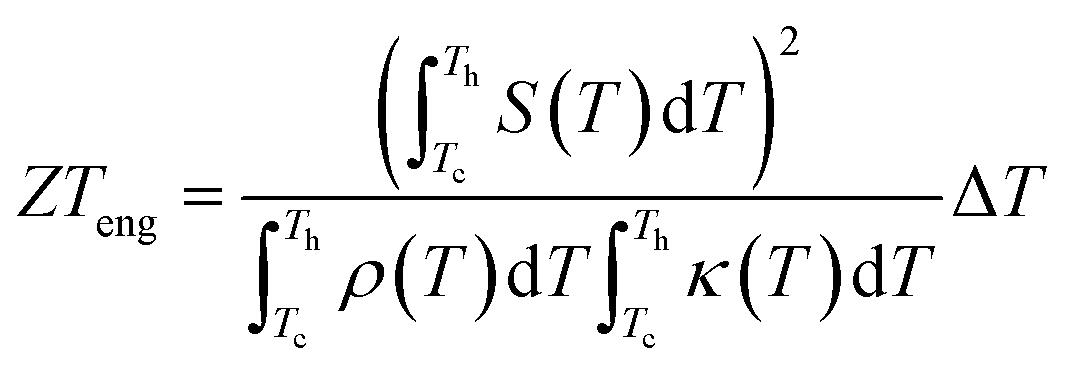
In addition, Fig. 7(a) shows that the samples synthesized through the alkaline earth metal reduction method are higher than those of Sb-doped Mg2Si1−xSnx based composites synthesized through traditional methods from the literature,20,22,33,34 particularly at high temperatures. Furthermore, the synthesis process is less time-consuming and simpler compared with the process of the optimal report.24
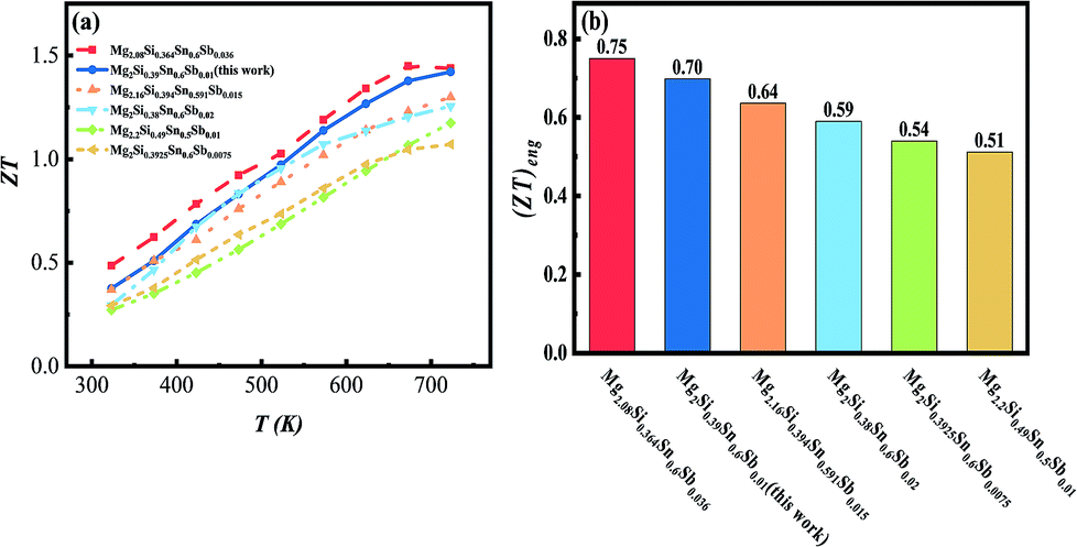 | ||
| Fig. 7 (a) Temperature-dependent ZTs and (b) engineering ZTs of optimal composite Mg2Si0.39Sn0.6Sb0.01 and the literature. | ||
Since the temperature-dependent ZTs of the thermoelectric materials varies in a wide temperature range, the engineering dimensionless figure-of-merit ((ZT)eng) proposed by Kim et al. was used to describe the average performance in the whole temperature, which is calculated based on the following equation:35
 | (7) |
Conclusion
In this work, a series of Sb-doped n-type Mg2Si0.4−xSn0.6Sbx (x = 0, 0.0075, 0.008, 0.009, 0.01, 0.011) bulk materials have been prepared using an alkaline earth metal reduction method through a combination of ball milling and an SPS process. The samples feature many dislocations at the grain boundaries, and plenty of nanoscale-coherent Mg2Si–Mg2Sn spinodal phases, both of which can effectively scatter heat-carrying phonons and do little to impact carrier transport. Meanwhile, the Sb-dopant can efficiently optimize the carrier concentration and significantly suppress the bipolar effects. As a result, a maximal ZT of 1.42 at 723 K and a maximal (ZT)eng of 0.7 with Tc = 323 K and Th = 723 K are obtained at the optimal Sb-doping level of x = 0.01, which is a competitive synthesis process compared with previous reports.20,22,24,33,34 This result proved that the thermoelectric performance of Mg2Si0.4Sb0.6 could be enhanced by defect engineering through an alkaline earth metal reduction method combined with the SPS process.Conflicts of interest
The authors have no conflicts to declare.Acknowledgements
This work was financially supported by the National Key Research and Development Plan (No. 2018YFE0306101 and 2016YFB0701301), the National Natural Science Foundation of China (No. U1601213 and 51572287), and the Key Research Program of Frontier Sciences of the Chinese Academy of Sciences (Grant No. QYZDB-SSW-SLH013).Notes and references
- J. He and T. M. Tritt, Science, 2017, 357, eaak9997 CrossRef PubMed.
- J. Yang, L. Xi, W. Qiu, L. Wu, X. Shi, L. Chen, J. Yang, W. Zhang, C. Uher and D. J. Singh, npj Comput. Mater., 2016, 2, 15015 CrossRef CAS.
- M. Jonson and G. D. Mahan, Phys. Rev. B: Condens. Matter Mater. Phys., 1980, 21, 4223–4229 CrossRef CAS.
- J. Shuai, J. Mao, S. Song, Q. Zhu, J. Sun, Y. Wang, R. He, J. Zhou, G. Chen, D. J. Singh and Z. Ren, Energy Environ. Sci., 2017, 10, 799–807 RSC.
- J. Mao, J. Shuai, S. Song, Y. Wu, R. Dally, J. Zhou, Z. Liu, J. Sun, Q. Zhang, C. Dela Cruz, S. Wilson, Y. Pei, D. J. Singh, G. Chen, C. W. Chu and Z. Ren, Proc. Natl. Acad. Sci. U. S. A., 2017, 114, 10548–10553 CrossRef CAS PubMed.
- D. Li, H. Zhao, S. Li, B. Wei, J. Shuai, C. Shi, X. Xi, P. Sun, S. Meng, L. Gu, Z. Ren and X. Chen, Adv. Funct. Mater., 2015, 25, 6478–6488 CrossRef CAS.
- Y. Pei, H. Wang and G. J. Snyder, Adv. Mater., 2012, 24, 6125–6135 CrossRef CAS PubMed.
- G. Tan, L. D. Zhao and M. G. Kanatzidis, Chem. Rev., 2016, 116, 12123–12149 CrossRef CAS PubMed.
- C. Fu, T. Zhu, Y. Liu, H. Xie and X. Zhao, Energy Environ. Sci., 2015, 8, 216–220 RSC.
- C. Fu, S. Bai, Y. Liu, Y. Tang, L. Chen, X. Zhao and T. Zhu, Nat. Commun., 2015, 6, 8144 CrossRef PubMed.
- T. Zou, X. Qin, Y. Zhang, X. Li, Z. Zeng, D. Li, J. Zhang, H. Xin, W. Xie and A. Weidenkaff, Sci. Rep., 2015, 5, 17803 CrossRef CAS PubMed.
- S. Li, Y. Liu, F. Liu, D. He, J. He, J. Luo, Y. Xiao and F. Pan, Nano Energy, 2018, 49, 257–266 CrossRef CAS.
- K. Biswas, J. He, I. D. Blum, C. I. Wu, T. P. Hogan, D. N. Seidman, V. P. Dravid and M. G. Kanatzidis, Nature, 2012, 489, 414–418 CrossRef CAS PubMed.
- J. He, S. N. Girard, M. G. Kanatzidis and V. P. Dravid, Adv. Funct. Mater., 2010, 20, 764–772 CrossRef CAS.
- Y. Yu, D.-S. He, S. Zhang, O. Cojocaru-Mirédin, T. Schwarz, A. Stoffers, X.-Y. Wang, S. Zheng, B. Zhu, C. Scheu, D. Wu, J.-Q. He, M. Wuttig, Z.-Y. Huang and F.-Q. Zu, Nano Energy, 2017, 37, 203–213 CrossRef CAS.
- B. Poudel, Q. Hao, Y. Ma, Y. Lan, A. Minnich, B. Yu, X. Yan, D. Wang, A. Muto, D. Vashaee, X. Chen, J. Liu, M. S. Dresselhaus, G. Chen and Z. Ren, Science, 2008, 320, 634 CrossRef CAS PubMed.
- H.-S. Kim, S. I. Kim, K. H. Lee, S. W. Kim and G. J. Snyder, Phys. Status Solidi B, 2017, 254, 1600103 CrossRef.
- Z. Wang, G. Wang, R. Wang, X. Zhou, Z. Chen, C. Yin, M. Tang, Q. Hu, J. Tang and R. Ang, ACS Appl. Mater. Interfaces, 2018, 10, 22401–22407 CrossRef CAS PubMed.
- W. Liu, X. Tan, K. Yin, H. Liu, X. Tang, J. Shi, Q. Zhang and C. Uher, Phys. Rev. Lett., 2012, 108, 166601 CrossRef PubMed.
- Q. Zhang, J. He, T. J. Zhu, S. N. Zhang, X. B. Zhao and T. M. Tritt, Appl. Phys. Lett., 2008, 93, 102109 CrossRef.
- J. Jang, B. Ryu, S.-J. Joo, B.-S. Kim, B.-K. Min, H.-W. Lee, S.-D. Park, H. S. Lee and J. E. Lee, J. Alloys Compd., 2018, 739, 129–138 CrossRef CAS.
- W. Liu, X. Tang, H. Li, K. Yin, J. Sharp, X. Zhou and C. Uher, J. Mater. Chem., 2012, 22, 13653 RSC.
- H. Zhao, B. Cao, S. Li, N. Liu, J. Shen, S. Li, J. Jian, L. Gu, Y. Pei, G. J. Snyder, Z. Ren and X. Chen, Adv. Energy Mater., 2017, 7, 1700446 CrossRef.
- G. Peng, I. Berkun, D. R. Schmidt, F. M. Luzenski, X. U. Lu and P. B. Sarac, J. Electron. Mater., 2014, 43, 1790–1803 CrossRef.
- W. Liu, X. Tang and J. Sharp, J. Phys. D: Appl. Phys., 2010, 43, 085406 CrossRef.
- D. Boudemagh, D. Fruchart, R. Haettel, E. K. Hlil, A. Lacoste, L. Ortega, N. E. Skryabina, J. Toboła and P. Wolfers, Solid State Phenom., 2011, 170, 253–258 CAS.
- J. J. Gong, A. J. Hong, J. Shuai, L. Li, Z. B. Yan, Z. F. Ren and J. M. Liu, Phys. Chem. Chem. Phys., 2016, 18, 16566–16574 RSC.
- A. F. May, E. S. Toberer, A. Saramat and G. J. Snyder, Phys. Rev. B: Condens. Matter Mater. Phys., 2009, 80, 125205 CrossRef.
- X. Shi, Y. Pei, G. J. Snyder and L. Chen, Energy Environ. Sci., 2011, 4, 4086 RSC.
- H.-S. Kim, Z. M. Gibbs, Y. Tang, H. Wang and G. J. Snyder, APL Mater., 2015, 3, 041506 CrossRef.
- W. Hao, C. Jin, L. Tianqi, Z. Kunjie, L. Shan, L. Jun and Z. Huaizhou, Chin. Phys. B, 2018, 27, 047212 CrossRef.
- F. Hao, P. Qiu, Y. Tang, S. Bai, T. Xing, H.-S. Chu, Q. Zhang, P. Lu, T. Zhang, D. Ren, J. Chen, X. Shi and L. Chen, Energy Environ. Sci., 2016, 9, 3120–3127 RSC.
- W. Liu, X. Tang, H. Li, J. Sharp, X. Zhou and C. Uher, Chem. Mater., 2011, 23, 5256–5263 CrossRef CAS.
- X. Zhang, H. Liu, S. Li, F. Zhang, Q. Lu and J. Zhang, Mater. Lett., 2014, 123, 31–34 CrossRef CAS.
- H. S. Kim, W. Liu, G. Chen, C. W. Chu and Z. Ren, Proc. Natl. Acad. Sci. U. S. A., 2015, 112, 8205–8210 CrossRef CAS PubMed.
| This journal is © The Royal Society of Chemistry 2019 |