
 Open Access Article
 This Open Access Article is licensed under a
 Creative Commons Attribution 3.0 Unported Licence
Pressure-induced metallization in MoSe2 under different pressure conditions†
Linfei Yangab,
Lidong Dai *a,
Heping Lia,
Haiying Hua,
Kaixiang Liuab,
Chang Puab,
Meiling Hongab and
Pengfei Liuc
*a,
Heping Lia,
Haiying Hua,
Kaixiang Liuab,
Chang Puab,
Meiling Hongab and
Pengfei Liuc
aKey Laboratory of High-Temperature and High-Pressure Study of the Earth's Interior, Institute of Geochemistry, Chinese Academy of Sciences, Guiyang, Guizhou 550081, China. E-mail: dailidong@vip.gyig.ac.cn
bUniversity of Chinese Academy of Sciences, Beijing 100049, China
cState Key Laboratory of Structural Chemistry, Fujian Institute of Research on the Structure of Matter, Chinese Academy of Sciences, Fuzhou, Fujian 350002, China
First published on 15th February 2019
Abstract
In this study, the vibrational and electrical transport properties of molybdenum diselenide were investigated under both non-hydrostatic and hydrostatic conditions up to ∼40.2 GPa using the diamond anvil cell in conjunction with Raman spectroscopy, electrical conductivity, high-resolution transmission electron microscopy, atomic force microscopy, and first-principles theoretical calculations. The results obtained indicated that the semiconductor-to-metal electronic phase transition of MoSe2 can be extrapolated by some characteristic parameters including abrupt changes in the full width at half maximum of Raman modes, electrical conductivity and calculated bandgap. Under the non-hydrostatic condition, metallization occurred at ∼26.1 GPa and it was irreversible. However, reversible metallization occurred at ∼29.4 GPa under the hydrostatic condition. In addition, the pressure-induced metallization reversibility of MoSe2 can be revealed by high-resolution transmission electron and atomic force microscopy of the recovered samples under different hydrostatic conditions. This discrepancy in the metallization phenomenon of MoSe2 in different hydrostatic environments was attributed to the mitigated interlayer van der Waals coupling and shear stress caused by the insertion of pressure medium into the layers.
Introduction
The AB2-type (A = Mo, W; B = S, Se, Te) transition-metal dichalcogenides (TMDs) have gained much interest owing to their unique mechanical, optical and electrical properties, and are widely used as solid-state lubricants, photodetectors, and transistors.1–3 Under ambient conditions, most of the transition-metal dichalcogenides possess a well-defined layered structure, in which the molecules are connected by the intralayer covalent bond and the interlayer van der Waals (vdW) forces. As an essential parameter, pressure can induce some changes in structural and electrical properties such as phase transition, amorphization and metallization in TMDs, and hence, pressure is of utmost importance for application in electromechanical devices, energy-variable opto-electronics and photovoltaics.4–8 Molybdenum diselenide (MoSe2) is one of the typical AB2-type TMDs with an indirect bandgap of ∼1.10 eV, crystallizing into a stable hexagonal 2Hc structure (space group: P63/mmc) under ambient conditions.9 A systematic work on the high-pressure behaviour of MoSe2 can be helpful in understanding the crystalline structure evolution and electrical properties of AB2-type layered materials, and also promotes its industrial exploitation in electronic devices.The high-pressure vibrational, structural and electrical properties for MoSe2 have been previously investigated by Raman and infrared spectroscopy, electrical resistivity and first-principles theoretical calculations. All of these results indicated that MoSe2 underwent a pressure-induced electronic transition from being a semiconductor to a metal. However, with regard to the metallization pressure point, there are many controversial viewpoints reported in previous studies. Rifliková et al. conducted the first-principles theoretical calculations up to 130 GPa to study the effect of high pressure on the evolution of the crystal structure and electronic properties of MoSe2, and predicted that it should undergo metallization at a pressure of at least ∼28 GPa.10 Caramazza et al. investigated the high-pressure optical properties of MoSe2 up to ∼30 GPa by means of Raman spectroscopy, and reported a pressure of ∼18 GPa for metallization with the pressure medium of NaCl.11 Dybala et al. measured the photoreflectance (PR) spectra of MoSe2 to explore its electronic band structure under hydrostatic pressure up to ∼20 GPa, and found that the metallization of MoSe2 occurred at ∼18 GPa with the pressure medium of liquid Daphne 7474.12 Zhao et al. investigated the high-pressure electrical transport behaviour of MoSe2 up to ∼60 GPa through the temperature-dependent electrical resistivity measurements, and their study results indicated that the metallization process was complete at ∼40 GPa using the pressure medium of cubic BN.7
In addition, as an important influential factor, the pressure environments can result in many structural and electronic property variations in the binary layered TMDs (e.g. WS2, MoS2 and ReS2). In the case of WS2, Duwal et al. confirmed that the isostructural phase transition from 2Hc to 2Ha occurred at ∼37 GPa under the non-hydrostatic condition, and however, under the hydrostatic condition, the phase structure was always stable with He being used as the pressure medium.13 Zhuang et al. observed a novel phenomenon that metallization of MoS2 was irreversible under the non-hydrostatic condition, while it was reversible under the hydrostatic condition.14 Zhuang et al. also found that metallization of ReS2 under the hydrostatic condition occurred at a much higher pressure point than that under the non-hydrostatic condition.15 As a similar layered structural diselenide, viz. MoSe2, it is possible that its high-pressure vibrational and electrical properties will be affected by different hydrostatic environments. However, till date, there are no relative reports on high-pressure structural and electronic properties in MoSe2 under different hydrostatic environments. Thus, further systematic investigation on MoSe2 is indispensable to explore the physical properties under different pressure environments.
In the present study, we report a semiconductor-to-metal transition of MoSe2 under non-hydrostatic and hydrostatic conditions of up to ∼40.2 GPa by virtue of a series of research methods including Raman spectroscopy, electrical conductivity, atomic force microscopy (AFM), high-resolution transmission electron microscopy (HRTEM) and first-principles calculations. Additionally, it was found that the metallization of MoSe2 was irreversible under the non-hydrostatic condition, but reversible under the hydrostatic condition. Furthermore, the reason for the diverse electrical properties displayed by MoSe2 under different pressure environments has been discussed in detail.
Experimental
MoSe2 powder samples with a high purity of 99.99% were commercially purchased from Leshan Kaiyada limited company. The X-ray diffraction (XRD) analysis of the powders was performed using an X'Pert Pro X-ray powder diffractometer (Phillips; Cu Kα, 45 kV, 40 mA). The X-ray powder diffraction pattern of crystal MoSe2 is shown in Fig. S1 (ESI†) under ambient conditions. High-pressure Raman spectroscopy and electrical conductivity experiments were carried out using the diamond anvil cell (DAC) with two symmetric anvil culets of 300 μm. In this study, helium was used for all the hydrostatic measurements and no pressure-transmitting medium was adopted for the non-hydrostatic experiments. Pressure calibration was conducted by virtue of the wavenumber shift of ruby fluorescence peaks.16 The uncertainties of pressure calibration under non-hydrostatic and hydrostatic conditions were less than 5% and 3%, respectively. The Raman spectroscopic measurements at room temperature and high pressure conditions were performed using a Renishaw 2000 micro-confocal Raman spectrometer equipped with the 514.5 nm argon ion laser and the 20 mW laser power. Each Raman spectroscopy was gathered in the frequency shift range of 150–400 cm−1 with a spectral resolution of ∼1.0 cm−1, and the collection time for each spectrum was ∼120 s. As for electrical conductivity measurements at room temperature and high pressure conditions, a T-301 stainless steel was employed as the gasket and pre-indented to a thickness of 50 μm beforehand, and then a 180 μm hole was drilled in the centre of the gasket by the laser drilling technique. The mixture of boron nitride (BN) and epoxy was compressed into the hole as the insulator, and another hole of 100 μm was then drilled to provide an insulated sample chamber. The electrical conductivity measurements were carried out by two-electrode method using a Solartron-1260 impedance/gain phase analyzer in the frequency range from 10−1 to 107 Hz. The temperature-dependent electrical conductivity measurements were performed in the temperature range from 120 K to 300 K. Similar to the experimental technique by Rahman et al., the in situ high-pressure electrical resistivity experiment is valid up to 55 GPa in the diamond anvil cell.17 More detailed descriptions on the experimental procedures and measurement methods have been reported previously.18–20Some microscopical observations on the recovered samples were performed at room temperature and high pressure conditions by virtue of the cross-sectional selected-area high-resolution transmission electron and atomic force microscopy. All of the acquired data via atomic force microscopy (AFM) and high-resolution transmission electron microscopy (HRTEM) images were collected using a Multimode 8 mass spectrometer (Bruker) and Tecnai G2 F20 S-TWIN TMP, respectively. The first-principles calculations were conducted on the basis of the density functional theory and pseudopotential methods, which were performed using the CASTEP code in the Material Studio package. The generalized gradient approximations (GGA) in the Perdew–Burke–Ernzerhof (PBE) scheme were applied for the description of the exchange and correlation terms. Structural optimizations were implemented using the Broyden–Fletcher–Goldfarb–Shanno (BFGS) minimization algorithm. In order to ensure high convergence of the enthalpy calculations, the cutoff energy and K-point grid were set to 950 eV and 24 × 24 × 8, respectively.
Results and discussion
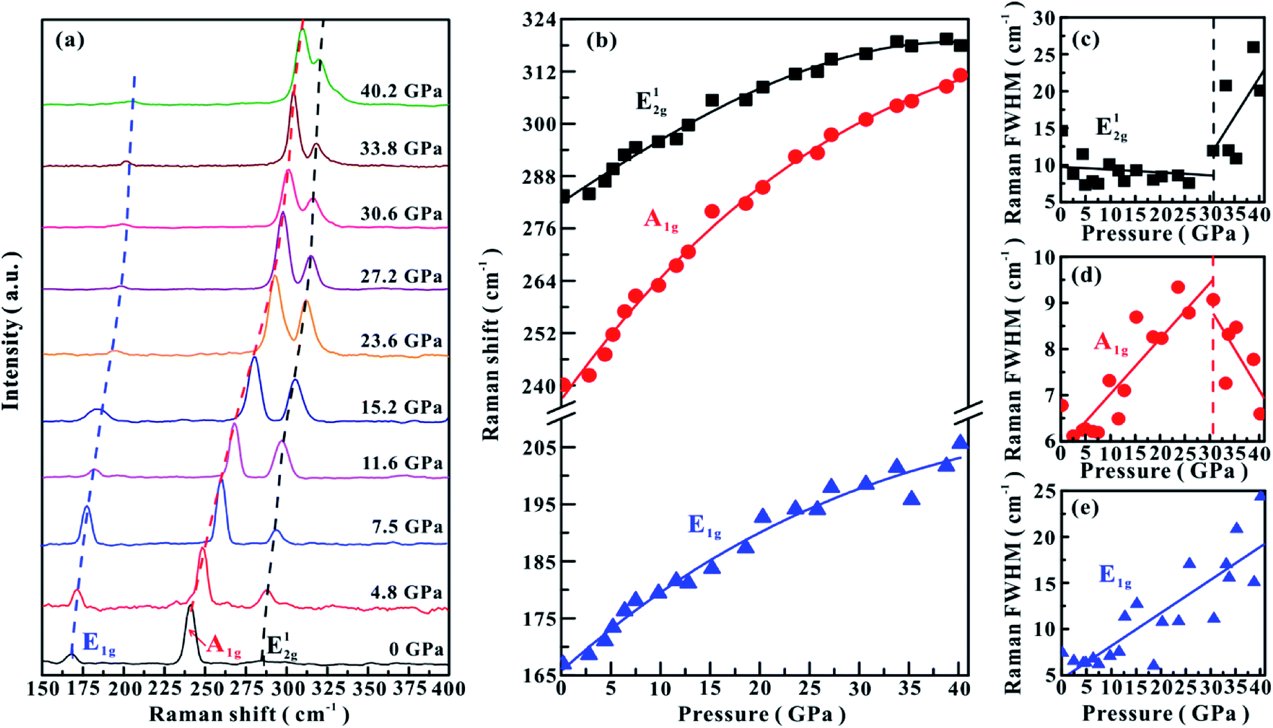
The high-pressure vibrational properties of MoSe2 were explored using Raman spectroscopy up to ∼40.2 GPa at room temperature. Raman spectra of MoSe2 were measured under both non-hydrostatic and hydrostatic conditions, and the corresponding results are displayed in Fig. 1a and 2a, respectively. Under ambient conditions, three typical Raman-active modes in MoSe2 were observed: A1g (241 cm−1), E1g (168 cm−1) and E12g (285 cm−1), which are in good agreement with previously reported results.21,22 A1g is an out-of-plane vibrational mode associated with the weak interlayer vdW interactions, while E1g and E12g are in-plane vibrational modes related to the strong intralayer covalent bonds.12 | ||
| Fig. 1 (a) Raman spectra of MoSe2 at representative pressure points under the non-hydrostatic condition. (b) The Raman shifts of three vibrational modes with increasing pressure. (c)–(e) The pressure dependence of FWHM for E12g, A1g and E1g, respectively. The dashed and solid lines serve as visual guides. | ||
 | ||
| Fig. 2 (a) Raman spectroscopic results of MoSe2 at representative pressure points under the hydrostatic condition. (b) The Raman shifts of three vibrational modes with increasing pressure. (c)–(e) The pressure dependence of FWHM for E12g, A1g and E1g, respectively. The dashed and solid lines serve as visual guides. | ||
Under the non-hydrostatic condition, as shown in Fig. 1b, all of these obtained modes monotonously shift to higher wave numbers with an increase in the pressure up to ∼40.1 GPa, showing no anomaly in the pressure-dependent Raman shifts. More specifically, it can be seen that these vibrational modes shift at different rates: the A1g mode shifts at much larger rate than E1g and E12g modes. However, according to the variations in the full-width at half-maximum (FWHM) for E12g and A1g modes, one distinct inflection point was obtained at a pressure of ∼25.0 GPa. The FWHM of E12g mode gradually decreases in the pressure range of 0–25.0 GPa, but increases with pressure in the range of 25.0–40.1 GPa (Fig. 1c). The FWHM of A1g mode displays different pressure dependence: it increases with pressure below ∼25.0 GPa, but decreases with pressure above ∼25.0 GPa (Fig. 1d). The FWHM of E1g mode continuously shifts to higher wave numbers with pressure (Fig. 1e). Under the hydrostatic condition, the pressure-dependent Raman shifts of three modes show monotonously increasing trends, and no anomalous pressure point was observed up to ∼40.2 GPa (Fig. 2b). As for the FWHM of E12g and A1g modes, we obtained a discontinuous point at a higher pressure of ∼30.6 GPa than those observed under the non-hydrostatic condition (Fig. 2c and d). The E1g mode exhibits a monotonously increasing tendency with pressure in the FWHM (Fig. 2e).
In terms of these observed discontinuities in the FWHM of E12g and A1g modes, Raman spectroscopy is one efficient method in determining the metallization of MoSe2 since the FWHM of these modes are directly associated with the charge transfer processes, which has been widely used to probe the metallization process in other materials.6,23 However, the metallization pressures under non-hydrostatic and hydrostatic conditions are determined to be ∼25.0 and ∼30.6 GPa, respectively. The discrepancy in the metallization pressure points was possibly related to the deviatoric stress. Under the non-hydrostatic condition, there exists strong deviatoric stress in the sample chamber (as displayed in Fig. S2,† the deviatoric stress reaches ∼5 GPa when the centre pressure is ∼39.6 GPa), which facilitates the occurrence of metallization by accelerating the reduction of the interlayer distances. However, for the hydrostatic condition, this electronic transition is delayed due to the protection by the pressure medium, which enters into the interlayer space and thus weakens the deviatoric stress.
The room-temperature and high-pressure electrical conductivity measurements have been implemented to explore the electrical behaviour of MoSe2 under the non-hydrostatic condition. The representative impedance spectra of MoSe2 up to ∼40.2 GPa are presented in Fig. 3a–c. In the pressure range of 1.0–14.8 GPa, the impedance spectra exhibit one approximately semicircular arc at high frequencies and another small semicircular arc at low frequencies, which stand for the grain interior and grain boundary contribution, respectively (Fig. 3a and b). Both semicircular arcs gradually decrease with the increase in the pressure from ∼1.0 to ∼14.8 GPa, and the grain boundary contribution of the sample becomes weaker. When the pressure is enhanced to ∼17.7 GPa, as shown in Fig. 3c, the grain boundary arc disappears and only the grain interior semicircular arc appears in the fourth quadrant, implying the occurrence of pressure-induced electronic polarization.24 Fig. 3d shows the pressure-dependent electrical conductivity of MoSe2 in the process of compression and decompression. One evident discontinuous point is observed at a pressure of ∼25.6 GPa upon compression. The electrical conductivity of the sample continuously increases in the pressure range of 1.0–25.6 GPa, but it tends to be stable with a relatively high value of ∼2.0 S cm−1 in the pressure range of 28.9–40.2 GPa. This available discontinuity of the electrical conductivity provides a robust evidence for the metallization of MoSe2 at ∼25.6 GPa, and this pressure point is consistent with the above-mentioned FWHM results under the non-hydrostatic condition. Upon decompression, the electrical conductivity of MoSe2 still remains at a very high value of ∼1.0 S cm−1, providing a crucial clue that the metallization is irreversible. This pressure-induced irreversible metallization is a very novel phenomenon, which has also been confirmed to occur in some other layered materials, such as MoS2, α-As2Te3 and Sb2S3.14,18,19
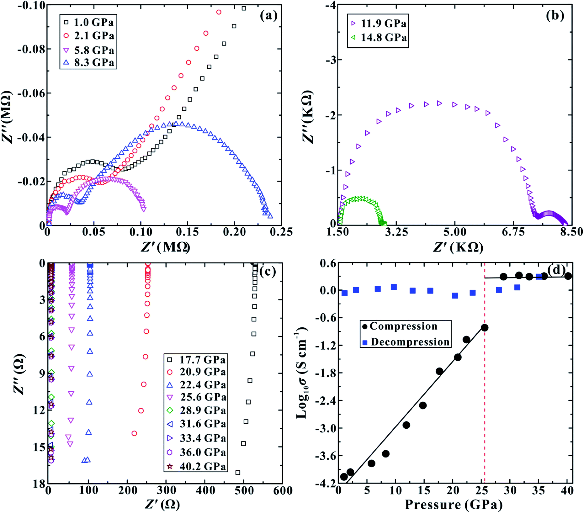 | ||
| Fig. 3 (a)–(c) The impedance spectra of MoSe2 in pressure ranges of 1.0–40.2 GPa. The horizontal and vertical axes represent the real and imaginary parts of the complex impedance, respectively. (d) The pressure dependence of electrical conductivity for MoSe2 in the process of compression and decompression. | ||
In order to further verify the metallization pressure point and examine whether MoSe2 endures an irreversible metallization, a series of temperature-dependent electrical conductivity measurements were carried out under the non-hydrostatic condition. Furthermore, we also conducted the temperature-dependent electrical conductivity measurements under the hydrostatic condition for comparisons. Generally, the semiconductor exhibits a positive relationship between electrical conductivity and temperature, while the metal does the opposite.25,26 Under the non-hydrostatic condition, the temperature dependence of electrical conductivity at various pressure points is shown in Fig. 4a. In the pressure range below ∼26.1 GPa, the electrical conductivity of MoSe2 increases with the increase in temperature, displaying a typical semiconductor characterization (Fig. 4b). By contrast, the electrical conductivity decreases with the increase in temperature above ∼26.1 GPa, indicating the occurrence of metallization at this point (Fig. 4c). Furthermore, it can be clearly observed from Fig. 4d that the sample still retains the metallic state after decompression, which further confirmed the irreversible metallization property for MoSe2 under these conditions. However, some different metallization characteristics of MoSe2 are obtained under the hydrostatic condition. As shown in Fig. 5a–c, the metallization pressure point is determined to be ∼29.4 GPa, which is higher than that observed under the non-hydrostatic condition, and the delay of metallization under the hydrostatic condition is in agreement with the above-mentioned FWHM results. Contrary to the irreversible metallization under the non-hydrostatic condition, MoSe2 undergoes a reversible metallization upon decompression under the hydrostatic condition (Fig. 5d). In a similar study, Zhao et al. observed the metallization phenomenon using the cubic boron nitride as the pressure medium for MoSe2 at a higher pressure of ∼40 GPa.7 It is possibly related to different experimental methods and pressure media, which can result in a discrepancy of metallization pressure points reported by us and Zhao et al.
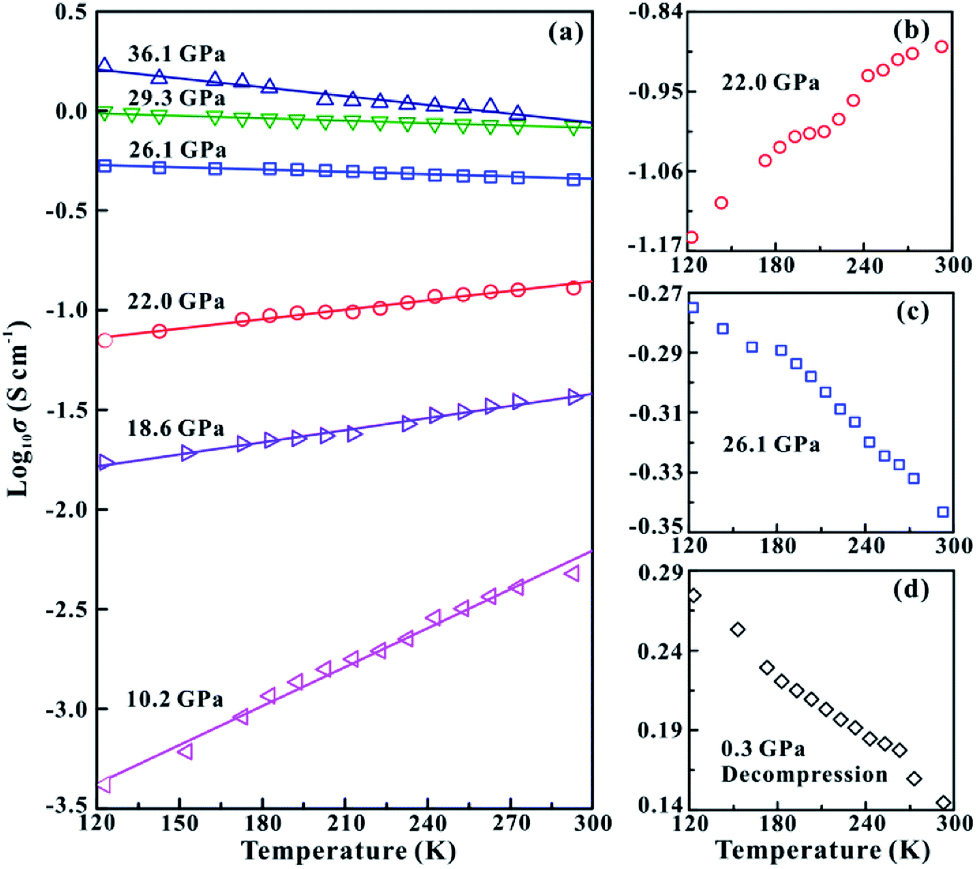 | ||
| Fig. 4 (a) The temperature-dependent electrical conductivity of MoSe2 at different pressure points under the non-hydrostatic condition. (b) The semiconducting state of MoSe2 at ∼22.0 GPa. (c) The metallization of MoSe2 at ∼26.1 GPa. (d) The metallic state of MoSe2 after decompression. | ||
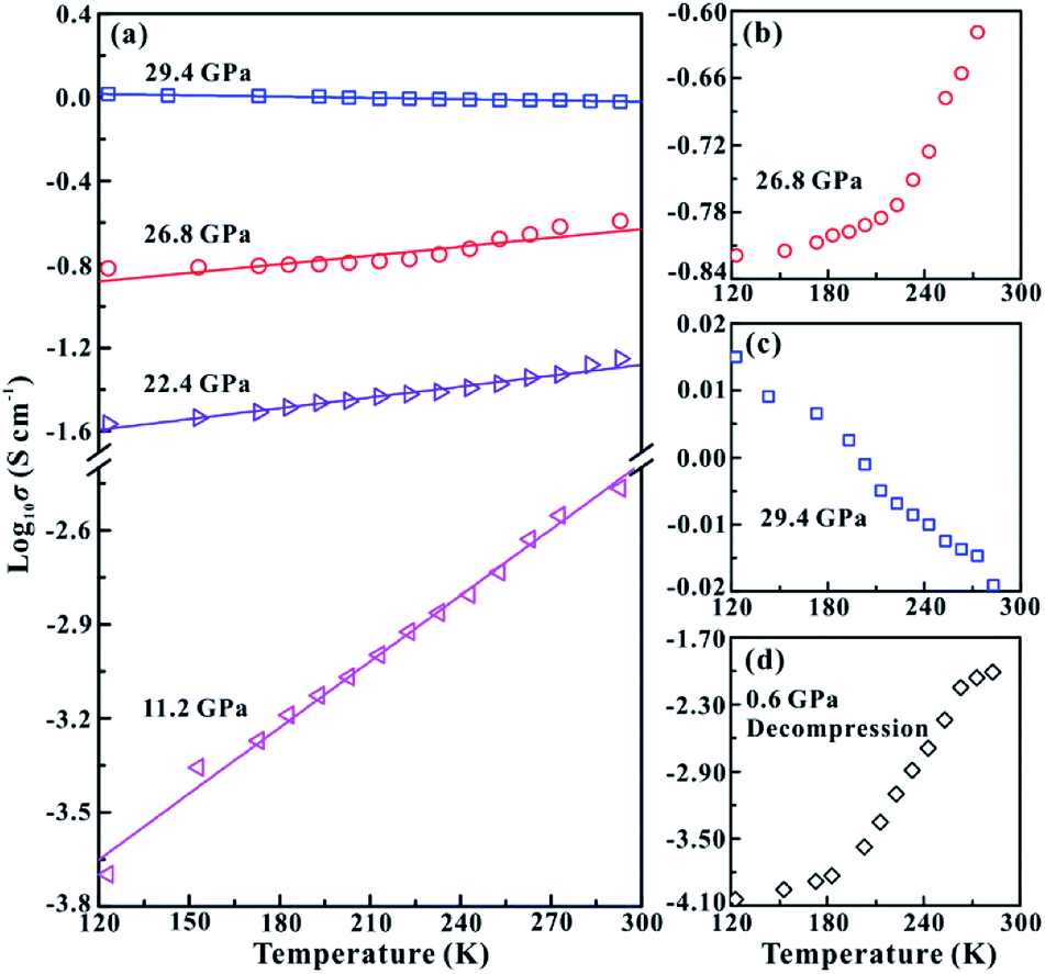 | ||
| Fig. 5 (a) The temperature dependence of electrical conductivity for MoSe2 at different pressure points under the hydrostatic condition. (b) The semiconducting state of MoSe2 at ∼26.8 GPa. (c) The metallization of MoSe2 at ∼29.4 GPa. (d) The semiconducting state of MoSe2 after decompression. | ||
Our electrical conductivity experimental results clearly indicate that the metallization behaviour of MoSe2 exhibits significant dependence on the pressure environments: under the hydrostatic condition, the metallization of MoSe2 occurs at ∼29.4 GPa and is reversible, while that under the non-hydrostatic condition occurs at a relatively lower pressure of ∼26.1 GPa and is irreversible. The key to understand these discrepancies in the metallization phenomenon is to figure out the states of the deviatoric stress and interlayer interaction under different hydrostatic environments, which have been proved to be very critical factors in influencing the metallization process of other similar layered materials.13,14 For the hydrostatic condition, the use of helium as the pressure-transmitting medium can alleviate the deviatoric stress and interlayer interaction through the injection of this medium into the interlayer space under high pressure. As a result, the delay of metallization occurs in the process of compression, and the interlayer distance recovers with the escape of pressure medium molecules from the layers after decompression. By contrast, strong deviatoric stress and interlayer interactions are generated within the vdW gap under the non-hydrostatic condition, which facilitates the occurrence of metallization and gives rise to the permanently plastic deformation of the interlayer spacing and thus the irreversible metallization.
To further check the pressure-induced metallization reversibility of MoSe2, we employed HRTEM and AFM to reveal the changes in the structure and morphology of recovered samples after decompression. From the HRTEM presented in Fig. 6a, the observed layers of the initial sample show a ∼0.64 nm interlayer spacing, which corresponds to the (002) oriented crystal planes of MoSe2 and is in good agreement with previous results.27,28 In the meantime, the corresponding fast Fourier transform (FFT) pattern is plotted in Fig. 6b, indicating the highly crystalline structure of the initial sample. After decompression from ∼40.0 GPa under the non-hydrostatic condition, the interlayer spacing of the sample drastically decreases to ∼0.23 nm (Fig. 6c). The corresponding FFT pattern shows a relatively weak halo ring of the (002) crystal planes, implying a low-degree crystalline structure for MoSe2 after the non-hydrostatic compression (Fig. 6d). However, under the hydrostatic condition, the recovered sample exhibits a well-discernible layered structure with an interlayer spacing of ∼0.60 nm, and the FFT pattern reveals a well-preserved crystal structure for the recovered MoSe2 after the hydrostatic compression (Fig. 6e and f). This indicated that the change in the interlayer spacing is irrevocable under the non-hydrostatic conditions; as a result, the irreversible metallization is observed. However, owing to the introduction of the pressure medium molecules in the interlayer spacing, the interlayer interactions and deviatoric stress are alleviated, causing the change in interlayer spacing to be recoverable under the hydrostatic condition and thus the reversible metallization of MoSe2. Meanwhile, according to the analysis of AFM, the surface morphology of recovered samples shows some significant differences under non-hydrostatic and hydrostatic conditions (Fig. 7a and b). After decompression from ∼37.5 GPa under the non-hydrostatic condition, the surface morphology of MoSe2 was very lumpy and the layered structure was destroyed. In contrast, for the recovered sample under the hydrostatic condition, the layered structure of MoSe2 could be well preserved as a result of the protection of the pressure medium. All of the HRTEM and AFM results provide favourable evidences for the irreversible metallization under the non-hydrostatic condition and reversible metallization under the hydrostatic condition.
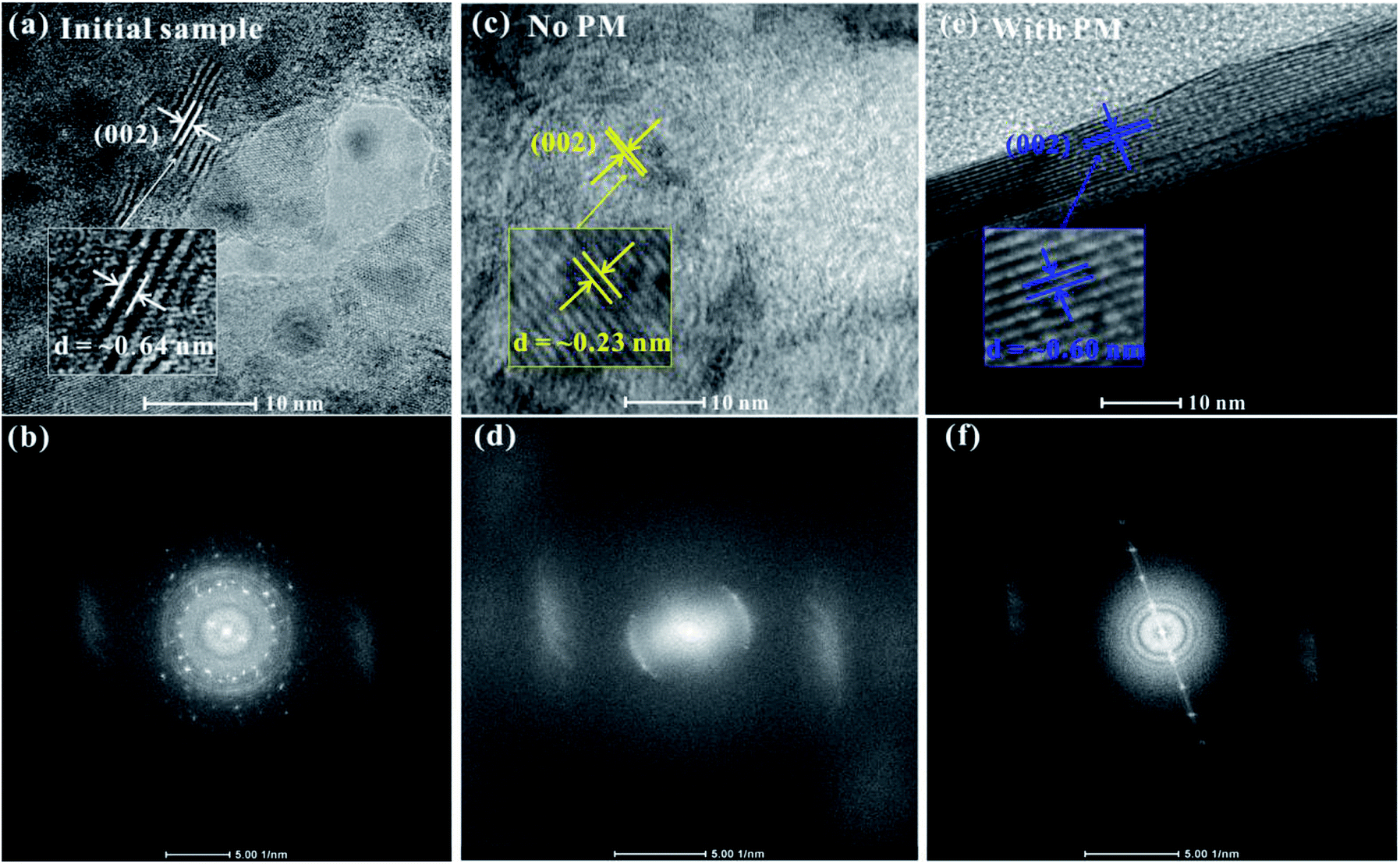 | ||
| Fig. 6 (a), (c) and (e) The HRTEM image of the starting sample, the recovered MoSe2 after decompression from ∼40.0 GPa under the non-hydrostatic condition, and the recovered MoSe2 after decompression from ∼39.6 GPa under the hydrostatic condition, respectively. (b), (d) and (f) The corresponding fast Fourier transform (FFT) pattern. Scale bar, 10 nm. | ||
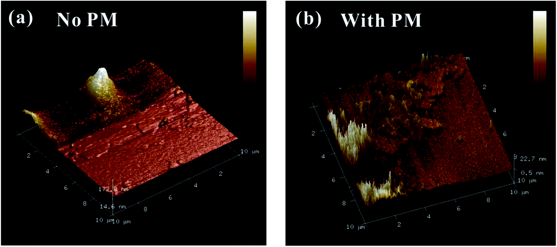 | ||
| Fig. 7 (a) AFM images of decompressed MoSe2 from ∼37.5 GPa under the non-hydrostatic condition. (b) AFM images of decompressed MoSe2 from ∼38.8 GPa under the hydrostatic condition. | ||
The theoretical calculations were implemented to predict the electronic and structural evolutions of MoSe2 under high pressure. Fig. 8 presents the predicted band structure, total density and projected density of MoSe2 at three representative pressure points (0, 10 and 28 GPa). As shown in Fig. 8a, the calculated band structure results clearly reveal a semiconducting ground state for MoSe2 with a bandgap of 1.24 eV at atmospheric pressure, which is slightly higher by ∼0.2 eV than the previously reported result.29 According to first-principles theoretical calculations by Ruiz-Fuertes et al., the feeble discrepancy is tolerant.30 The corresponding density of state for MoSe2 at atmospheric pressure is plotted in Fig. 8b. The valence bands between about −15 and −12 eV are predominantly composed of the Se-s state. From about −6 to 0 eV, the valence bands are composed of Se-s, Se-p, Mo-s, Mo-p, and Mo-d states, which are mutually hybridized and dominated by the Se-p and Mo-d states. Above the Fermi-level (EF), the lowest conduction bands from about 0 to 5 eV are dominated by the Mo-d and Se-p states, and the highest conduction bands from about 5 to 10 eV are mainly composed of the Se-s state. When the pressure is enhanced to 20 GPa, the bandgap of MoSe2 decreases to 0.22 eV (Fig. 8c). Meanwhile, all of these energy bands have been expanded at this pressure point, and the high-energy valence bands widen more than the conduction bands (Fig. 8d). Upon further compression to 28 GPa, the bandgap reaches a critical value of 0 eV, and an overlap between valence and conduction bands can be clearly observed (Fig. 8e and f), showing the metal characteristic for MoSe2. Fig. 9d displays the predicted pressure dependence of the bandgap up to 40 GPa. The bandgap energy of MoSe2 shows a decreasing tendency with the increasing pressure and reaches 0 eV at a pressure of 28 GPa, an indication of metallization for MoSe2 at this pressure point. This predicted metallization pressure point by the generalized gradient approximation (GGA) is well consistent with our above-mentioned experimental results. However, its magnitude is obviously lower than that reported by Zhao et al., which was obtained by the HSE06 hybrid functional approximation.7 As usual, the bandgap energy might be overestimated by HSE06 hybrid functional approximation.10 In addition, the calculated pressure-dependent normalized cell parameters and volume of MoSe2 are presented in Fig. 9a and b. It can be clearly seen that all of these obtained crystalline parameters including a/a0, b/b0 and unit cell volume for MoSe2 gradually decrease with the increase in the pressure. Obviously, all available continuous variations between crystalline parameters and pressure realized that the occurrence of the pressure-induced metallization for MoSe2 is not triggered by the structural phase transition. We think that the metallization phenomenon of MoSe2 is closely associated with the pressure-induced reduction of the intralayer distance, i.e., with the increasing pressure, the distance of the neighbouring Se atom planes will be rapidly decreased, which results in the strong Se–Se interactions and further leads to the occurrence of metallization. In addition, a series of representative selenides with similar layered structures (e.g., InSe, GaSe, ReSe2 and SnSe2) have also been reported to undergo the phase transition of metallization under high pressure, and therefore, the pressure-induced metallization maybe widely existing in most of selenides.31–34
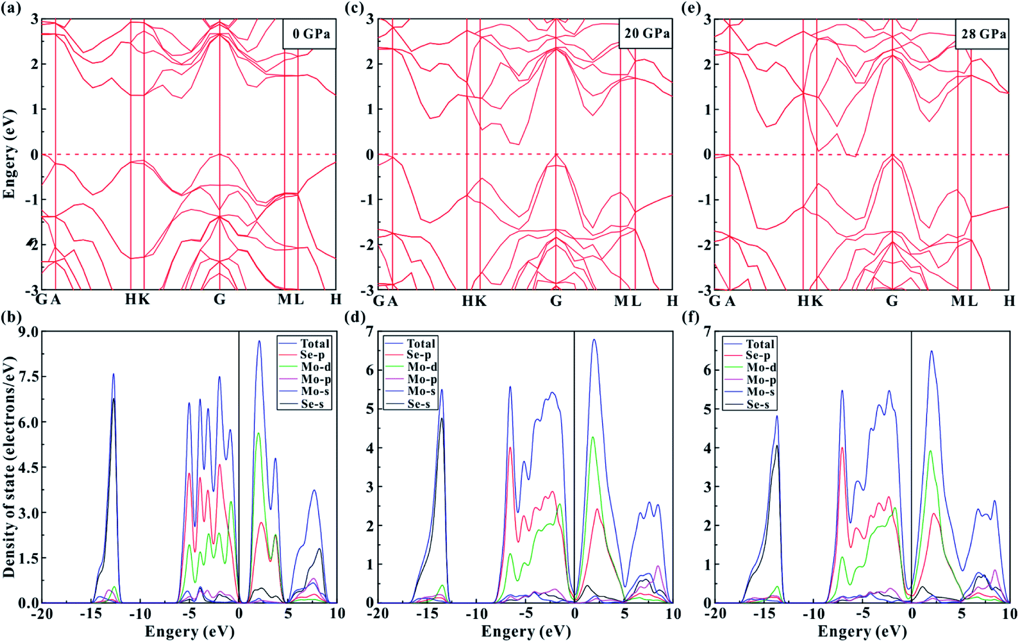 | ||
| Fig. 8 (a), (c) and (e) The calculated band structure of MoSe2 at representative pressures of ∼0, ∼20 and ∼28 GPa, respectively. (b), (d) and (f) The corresponding total density and projected density at ∼0, ∼20 and ∼28 GPa, respectively. | ||
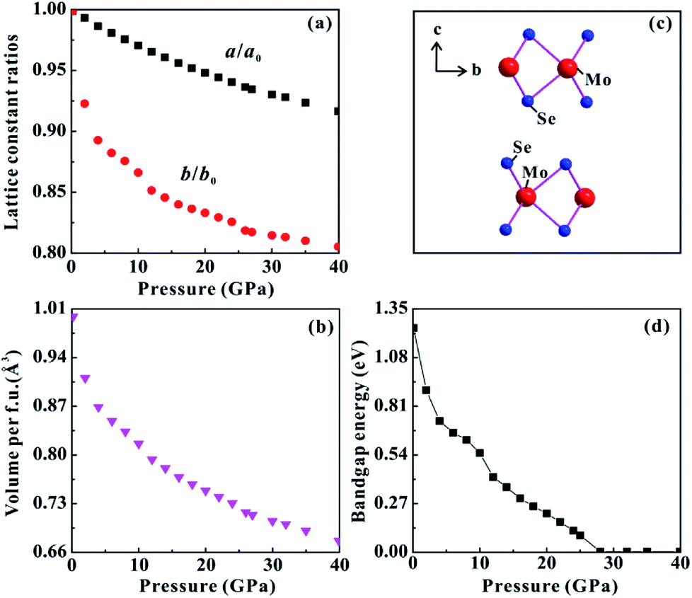 | ||
| Fig. 9 (a) The pressure-dependent a/a0 and c/c0 data of MoSe2 from theoretical calculations. (b) The calculated volume of MoSe2 versus pressure. (c) Crystalline structure of hexagonal (P63/mmc) crystal MoSe2 at ambient pressure. (d) The calculated bandgap of MoSe2 with increasing pressure up to 40.0 GPa. | ||
Conclusions
The high-pressure vibrational and electronic properties of MoSe2 were systematically investigated under non-hydrostatic and hydrostatic conditions using a diamond anvil cell in conjunction with Raman spectroscopy, electrical conductivity, atomic force microscopy, high-resolution transmission electron microscopy, and first-principles calculations. The results confirmed the electronic transition of MoSe2 from a semiconductor to a metal on the basis of the obvious changes in the FWHM of Raman modes, electrical conductivity and calculated bandgap energy. The metallization pressure points under non-hydrostatic and hydrostatic conditions were well determined to be ∼26.1 and ∼29.4 GPa, respectively. Interestingly, the metallization was irreversible under the non-hydrostatic condition, while that was reversible under the hydrostatic condition. The reversibility of metallization displayed by MoSe2 under different hydrostatic environments was attributed to the effect of pressure medium molecules, which played a critical role in determining whether the interlayer spacing can be restored upon decompression.Conflicts of interest
There are no conflicts to declare.Acknowledgements
This research was financially supported by the Strategic Priority Research Program (B) of the Chinese Academy of Sciences (XDB 18010401), Key Research Program of Frontier Sciences of CAS (QYZDB-SSW-DQC009), “135” Program of the Institute of Geochemistry of CAS, Hundred Talents Program of CAS and NSF of China (41474078, 41774099 and 41772042). The support of the Supercomputer Center of Fujian Institute of Research on the Structure of Matter (FJIRSM) is acknowledged.References
- L. Rapoport, Y. Bilik, Y. Feldman, M. Homyonfer, S. R. Cohen and R. Tenne, Hollow nanoparticles of WS2 as potential solid-state lubricants, Nature, 1997, 387, 791–793 CrossRef CAS.
- P. J. Ko, A. Abderrahmane, N. H. Kim and A. Sandhu, High-performance near-infrared photodetector based on nano-layered MoSe2, Semicond. Sci. Technol., 2017, 32, 065015 CrossRef.
- A. Ayari, E. Cobas, O. Ogundadegbe and M. S. Fuhrer, Realization and electrical characterization of ultrathin crystals of layered transition-metal dichalcogenides, J. Appl. Phys., 2007, 101, 014507 CrossRef.
- X. Wang, X. Chen, Y. Zhou, C. Park, C. An, Y. Zhou, R. Zhang, C. Gu, W. Yang and Z. Yang, Pressure-induced iso-structural phase transition and metallization in WSe2, Sci. Rep., 2017, 7, 46694 CrossRef CAS PubMed.
- P. G. Naumov, M. A. ElGhazali, H. Mirhosseini, V. Süβ, E. Morosan, C. Felser and S. A. Medvedev, Pressure-induced metallization in layered ReSe2, J. Phys.: Condens. Matter, 2018, 30, 035401 CrossRef CAS PubMed.
- A. P. Nayak, S. Bhattacharyya, J. Zhu, J. Liu, X. Wu, T. Pandey, C. Jin, A. K. Singh, D. Akinwande and J. F. Lin, Pressure-induced semiconducting to metallic transition in multilayered molybdenum disulphide, Nat. Commun., 2014, 5, 3731 CrossRef CAS PubMed.
- Z. Zhao, H. Zhang, H. Yuan, S. Wang, Y. Lin, Q. Zeng, G. Xu, Z. Liu, G. K. Solanki, K. D. Patel, Y. Cui, H. Y. Hwang and W. L. Mao, Pressure induced metallization with absence of structural transition in layered molybdenum diselenide, Nat. Commun., 2015, 6, 7312 CrossRef CAS PubMed.
- M. Brotons-Gisbert, A. Segura, R. Robles, E. Canadell, P. Ordejón and J. F. Sánchez-Royo, Optical and electronic properties of 2H-MoS2 under pressure: Revealing the spin-polarized nature of bulk electronic bands, Phys. Rev. Mater., 2018, 2, 054602 CrossRef.
- R. Coehoorn, C. Haas and R. A. de Groot, Electronic structure of MoSe2, MoS2, and WSe2 II. The nature of the optical band gaps, Phys. Rev. B: Condens. Matter Mater. Phys., 1987, 35, 6203–6206 CrossRef CAS.
- M. Rifliková, R. Martoňák and E. Tosatti, Pressure-induced gap closing and metallization of MoSe2 and MoTe2, Phys. Rev. B: Condens. Matter Mater. Phys., 2014, 90, 035108 CrossRef.
- S. Caramazza, F. Capitani, C. Marini, A. Mancini, L. Malayasi, P. Dore and P. Postorino, Effect of pressure on optical properties of the transition metal dichalcogenide MoSe2, J. Phys.: Conf. Ser., 2017, 950, 042012 CrossRef.
- F. Dybala, M. P. Polak, J. Kopaczek, P. Scharoch, K. Wu, S. Tongay and R. Kudrawiec, Pressure coefficients for direct optical transitions in MoS2, MoSe2, WS2, and WSe2 crystals and semiconductor to metal transitions, Sci. Rep., 2016, 6, 26663 CrossRef CAS PubMed.
- S. Duwal and C.-S. Yoo, Shear-induced isostructural phase transition and metallization of layered tungsten disulfide under nonhydrostatic compression, J. Phys. Chem. C, 2016, 120, 5101–5107 CrossRef CAS.
- Y. Zhuang, L. Dai, L. Wu, H. Li, H. Hu, K. Liu, L. Yang and C. Pu, Pressure-induced permanent metallization with reversible structural transition in molybdenum disulfide, Appl. Phys. Lett., 2017, 110, 122103 CrossRef.
- Y. Zhuang, L. Dai, H. Li, H. Hu, K. Liu, L. Yang, C. Pu, M. Hong and P. Liu, Deviatoric stresses promoted metallization in rhenium disulfide, J. Phys. D: Appl. Phys., 2018, 51, 165101 CrossRef.
- H. K. Mao, J. Xu and P. M. Bell, Calibration of the ruby pressure gauge to 800 kbar under quasi-hydrostatic conditions, J. Geophys. Res., 1986, 91, 4673–4676 CrossRef CAS.
- S. Rahman, H. Saqib, J. Zhang, D. Errandonea, C. Menéndez, C. Cazorla, S. Samanta, X. Li, J. Lu and L. Wang, Pressure-induced structural and semiconductor to semiconductor transitions in Co0.5Mg0.5Cr2O4, Phys. Rev. B, 2018, 97, 174102 CrossRef.
- L. Dai, Y. Zhuang, H. Li, L. Wu, H. Hu, K. Liu, L. Yang and C. Pu, Pressure-induced irreversible amorphization and metallization with a structural phase transition in arsenic telluride, J. Mater. Chem. C, 2017, 5, 12157–12162 RSC.
- L. Dai, K. Liu, H. Li, L. Wu, H. Hu, Y. Zhuang, L. Yang, C. Pu and P. Liu, Pressure-induced irreversible metallization accompanying the phase transitions in Sb2S3, Phys. Rev. B, 2018, 97, 024103 CrossRef.
- L. Wu, L. Dai, H. Li, H. Hu, Y. Zhuang and K. liu, Anomalous phase transition of Bi-doped Zn2GeO4 investigated by electrical conductivity and Raman spectroscopy under high pressure, J. Appl. Phys., 2017, 121, 125901 CrossRef.
- T. Sekine, M. Izumi, T. Nakashizu, K. Uchinokura and E. Matsuura, Raman-scattering and infrared reflectance in 2H-MoSe2, J. Phys. Soc. Jpn., 1980, 49, 1069–1077 CrossRef CAS.
- S. V. Bhatt, M. P. Deshpande, V. Sathe, R. Rao and S. H. Chaki, Raman spectroscopic investigations on transition-metal dichalcogenides MX2 (M = Mo, W; X = S, Se) at high pressures and low temperature, J. Raman Spectrosc., 2014, 45, 971–979 CrossRef CAS.
- C. Marini, D. Chermisi, M. Lavagnini, D. Di Castro, C. Petrillo, L. Degiorgi, S. Scandolo and P. Postorino, High-pressure phases of crystalline tellurium: a combined Raman and ab initio study, Phys. Rev. B: Condens. Matter Mater. Phys., 2012, 86, 064103 CrossRef.
- Y. A. Kandrina, A. N. Babushkin, S. N. Shkerin and Y. Volkova, Application of the AC impedance spectroscopy at high pressures: electrophysical properties of sulfur, Defect Diffus. Forum, 2002, 208–209, 295–298 CAS.
- Z. H. Chi, X. M. Zhao, H. Zhang, A. F. Goncharov, S. S. Lobanov, T. Kagayama, M. Sakata and X. J. Chen, Pressure-induced metallization of molybdenum disulfide, Phys. Rev. Lett., 2014, 113, 036802 CrossRef PubMed.
- G. Zhang, B. Wu, J. Wang, H. Zhang, H. Liu, J. Zhang, C. Liu, G. Gu, L. Tian, Y. Ma and C. Gao, Metallization and electrical transport behaviors of GaSb under high-pressure, Sci. Rep., 2017, 7, 2656 CrossRef PubMed.
- R. Harpeness, A. Gedanken, A. M. Weiss and M. A. Slifkin, Microwave-assisted synthesis of nanosized MoSe2, J. Mater. Chem., 2003, 13, 2603 RSC.
- M. Nath and C. N. R. Rao, MoSe2 and WSe2 nanotubes and related structures, Chem. Commun., 2001, 21, 2236–2237 RSC.
- J. Gusakova, X. Wang, L. L. Shiau, A. Krivosheeva, V. Shaposhnikov, V. Borisenko, V. Gusakov and B. K. Tay, Electronic properties of bulk and monolayer TMDs: theoretical study within DFT framework (GVJ-2e method), Phys. Status Solidi A, 2017, 214, 1700218 CrossRef.
- J. Ruiz-Fuertes, S. López-Moreno, J. López-Solano, D. Errandonea, A. Segura, R. Lacomba-Perales, A. Muñoz, S. Radescu, P. Rodríguez-Hernández, M. Gospodinov, L. L. Nagornaya and C. Y. Tu, Pressure effects on the electronic and optical properties of AWO4 wolframites (A = Cd, Mg, Mn, and Zn): the distinctive behavior of multiferroic MnWO4, Phys. Rev. B: Condens. Matter Mater. Phys., 2012, 86, 125202 CrossRef.
- D. Errandonea, D. Martínez-García, A. Segura, A. Chevy, G. Tobias, E. Canadell and P. Ordejon, High-pressure, high-temperature phase diagram of InSe: a comprehensive study of the electronic and structural properties of the monoclinic phase of InSe under high pressure, Phys. Rev. B: Condens. Matter Mater. Phys., 2006, 73, 235202 CrossRef.
- U. Schwarz, D. Olguin, A. Cantarero, M. Hanfland and K. Syassen, Effect of pressure on the structural properties and electronic band structure of GaSe, Phys. Status Solidi B, 2007, 244, 244–255 CrossRef CAS.
- P. G. Naumov, M. A. Eighazali, H. Mirhosseini, V. Süβ, E. Morosan, C. Felser and S. A. Medvedev, Pressure-induced metallization in layered ReSe2, J. Phys.: Condens. Matter, 2018, 30, 035401 CrossRef CAS PubMed.
- Y. Zhou, B. Zhang, X. Chen, C. Gu, C. An, Y. Zhou, K. Cai, Y. Yuan, C. Chen, H. Wu, R. Zhang, C. Park, Y. Xiong, X. Zhang, K. Wang and Z. Yang, Pressure-induced metallization and robust superconductivity in pristine 1T-SnSe2, Adv. Electron. Mater., 2018, 4, 1800155 CrossRef.
Footnote |
| † Electronic supplementary information (ESI) available. See DOI: 10.1039/c8ra09441a |
| This journal is © The Royal Society of Chemistry 2019 |