
 Open Access Article
 This Open Access Article is licensed under a Creative Commons Attribution-Non Commercial 3.0 Unported Licence
Synthesis of ternary oxide Zn2GeO4 nanowire networks and their deep ultraviolet detection properties
Xu Han abc,
Shuanglong Fengbc,
Yiming Zhaoabc,
Lei Libc,
Zhaoyao Zhan*bcd,
Zhiyong Taoa,
Yaxian Fan*a,
Wenqiang Lu*abc,
Wenbin Zuoe and
Dejun Fue
abc,
Shuanglong Fengbc,
Yiming Zhaoabc,
Lei Libc,
Zhaoyao Zhan*bcd,
Zhiyong Taoa,
Yaxian Fan*a,
Wenqiang Lu*abc,
Wenbin Zuoe and
Dejun Fue
aSchool of Physics, Key Laboratory of InFiber Integrated Optics, Ministry of Education of China, Harbin Engineering University, Harbin 150001, China. E-mail: yxfan@hrbeu.edu.cn; wqlu@cigit.ac.cn
bChongqing Key Laboratory of Multi-scale Manufacturing Technology, Chongqing Institute of Green and Intelligent Technology, Chinese Academy of Sciences, Chongqing 400714, China. E-mail: zhanhit@hotmail.com
cUniversity of Chinese Academy of Sciences, Beijing, China
dSchool of Mechanical and Aerospace Engineering, Nanyang Technological University, 50 Nanyang Ave., 639798, Singapore
eKey Laboratory of Artificial Micro, and Nano-Materials of Ministry of Education, School of Physics and Technology, Wuhan University, Wuhan 430072, China
First published on 11th January 2019
Abstract
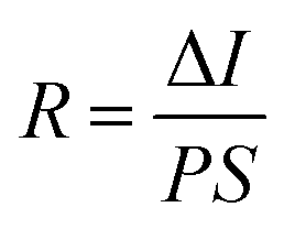
Ternary oxide Zn2GeO4 with a wide bandgap of 4.84 eV, as a candidate for fourth generation semiconductors, has attracted a great deal of attention for deep ultraviolet (DUV) photodetector applications, because it is expected to be blind to the UV-A/B band (290–400 nm) and only responsive to the UV-C band (200–290 nm). Here, we report on the synthesis of Zn2GeO4 nanowire (NW) networks by lower pressure chemical vapor deposition and investigate their corresponding DUV detection properties. We find that pure Zn2GeO4 NWs could be obtained at a growth pressure of 1 kPa. The DUV detection tests reveal that growth pressure exerts a significant effect on DUV detection performance. The Zn2GeO4 NW networks produced under 1 kPa show an excellent solar-blind photoresponsivity with fast rise and decay times (trise ≈ 0.17 s and tdecay ≈ 0.14 s).
1. Introduction
Recently, wide-bandgap metal oxide nanostructures have attracted extensive attention for potential application in next-generation electronics including transparent conductive electrodes, sensing elements, energy harvesting and storage devices, and optoelectronics.1–10 Among them, UV detection, especially, solar-blind deep ultraviolet (DUV) photodetection is emerging as a hot topic because of their wide applications in commercial and military fields, including flame or engine monitoring, environmental and biological research, space technology, and missile launch.11–18 To date, extensive attention has been paid to binary wide-bandgap materials for UV detection, such as ZnO,19 SnO2,20 ZnS,11–14 MnO3![[thin space (1/6-em)]](https://www.rsc.org/images/entities/char_2009.gif) 21 and AlN.22 However, much less effort has been devoted to more complex systems, such as ternary oxides, probably due to the difficulty with the preparation of high quality ternary nanostructures. Generally, ternary oxide systems are more chemically and thermally stable, and are more competitive candidates for deep UV detection due to their larger bandgap and hence higher photon energy thresholds. Recently, several ternary oxides including Zn2SnO4, In2Ge2O7, and ZnGa2O4 have been employed for DUV detection. Among these candidates, ternary oxide Zn2GeO4 has a wide bandgap of about 4.84 eV, which is expected to be blind to UV-A/B band (290–400 nm) and only responsive to UV-C band (200–290 nm).5,9,10 The Zn2GeO4 nanostructures, especially Zn2GeO4 nanowires (NWs), have attracted a great deal of attention because of large specific surface area,2,4,23 fast charge transport characteristics,24 and high optical absorption. To utilize their full potential in DUV photodetection, Zn2GeO4 NWs should be facilely fabricated and integrated into DUV photodetectors (PDs) with fast response speed in a cost-effective manner. At the same time, there is a huge possibility in the field of wearable devices with further exploration on flexible substrate as well as self-powered photodetector.25,26 Previously, we have proposed that the response speed of metal oxide NW-based UV PDs could be improved by directly growing entangled NW array grown on SiO2 by chemical vapor deposition (CVD). The interconnections in NW array creates NW–NW junction barriers which dominate the inter-wire charge transport. The UV illumination induces fast tuning of NW–NW junction barrier height, which contributes to the enhanced response speed of the NW-array UV PDs. Thus the Zn2GeO4 NW networks should bear great advantages in terms of PDs fabrication and also response speed.
21 and AlN.22 However, much less effort has been devoted to more complex systems, such as ternary oxides, probably due to the difficulty with the preparation of high quality ternary nanostructures. Generally, ternary oxide systems are more chemically and thermally stable, and are more competitive candidates for deep UV detection due to their larger bandgap and hence higher photon energy thresholds. Recently, several ternary oxides including Zn2SnO4, In2Ge2O7, and ZnGa2O4 have been employed for DUV detection. Among these candidates, ternary oxide Zn2GeO4 has a wide bandgap of about 4.84 eV, which is expected to be blind to UV-A/B band (290–400 nm) and only responsive to UV-C band (200–290 nm).5,9,10 The Zn2GeO4 nanostructures, especially Zn2GeO4 nanowires (NWs), have attracted a great deal of attention because of large specific surface area,2,4,23 fast charge transport characteristics,24 and high optical absorption. To utilize their full potential in DUV photodetection, Zn2GeO4 NWs should be facilely fabricated and integrated into DUV photodetectors (PDs) with fast response speed in a cost-effective manner. At the same time, there is a huge possibility in the field of wearable devices with further exploration on flexible substrate as well as self-powered photodetector.25,26 Previously, we have proposed that the response speed of metal oxide NW-based UV PDs could be improved by directly growing entangled NW array grown on SiO2 by chemical vapor deposition (CVD). The interconnections in NW array creates NW–NW junction barriers which dominate the inter-wire charge transport. The UV illumination induces fast tuning of NW–NW junction barrier height, which contributes to the enhanced response speed of the NW-array UV PDs. Thus the Zn2GeO4 NW networks should bear great advantages in terms of PDs fabrication and also response speed.
Usually, growth of Zn2GeO4 NWs is conducted under a very stringent condition (low pressure < 500 Pa, and high temperature ∼ 1000 °C).5,10 The effect of pressure on growth of Zn2GeO4 NWs and the corresponding solar blind UV detection properties have not been fully investigated. Generally, the growth rate of Zn2GeO4 NWs is proportional to the vapor pressure in the CVD system. In addition, low vacuum level is also easy to achieve and maintain. Thus it would be desirable to grow high quality Zn2GeO4 NWs at a relatively higher pressure. In this paper, we report on synthesis of Zn2GeO4 NW networks at relatively higher pressure and investigate their DUV detection properties. We find that the pure Zn2GeO4 NWs could be only obtained at a growth pressure of 1 kPa or lower pressure; the higher pressure could lead to growth of Zn2GeO4 NW networks with impurities but at a higher growth rate. The DUV detection tests also reveal that growth pressure exerted a significant effect on DUV detection performance. The Zn2GeO4 NW networks produced under 1 kPa shows an excellent solar-blind photoresponsivity such as fast rise and decay times (trise ≈ 0.17 s and tdecay ≈ 0.14 s) justifying the potential of the Zn2GeO4 nanowires for solar-blind DUV detection.
2. Experimental
Zn2GeO4 nanowires were synthesized via a facile CVD method. 0.421 g mixture of ZnO, GeO2, and diamond powders (molar ratio of 2:1:3) was loaded in a ceramic boat which is located at the center of quartz tube furnace. A piece of Si substrate (500 nm SiO2/Si) coated with 3 nm Au films was covered just above the source materials. 100 standard cubic centimeter per minute (sccm) Ar was introduced into the chamber as carrier gas. The tube furnace was then heated to 960 °C within 68 min. Once the temperature reached 600 °C, 1.5 sccm oxygen was introduced into the furnace. To evaluate the effect of pressure on Zn2GeO4 NW networks growth, the pressure in the chamber was set to 0.5 kPa, 1 kPa, 2 kPa, 5 kPa and 15 kPa, respectively. The furnace was kept at 960 °C for 15 min, and then the oxygen was switched off and the furnace was cooled naturally down to room temperature. After growth, a layer of white or gray materials were obtained on the SiO2/Si substrates. The final products were characterized and analyzed by a SEM (JSM-7800F, JEOL) equipped with an EDX detector, XRD (D8 ADVANCE, BRUCKER), and a HRTEM (Tecnai G2-F20, FEI). The Raman spectra were collected on a Renishaw system excited by an argon laser of 488 nm wavelength.
The devices were fabricated according to processes reported in our previous works.1,2,30 A two-end metal-semiconductor-metal structured Zn2GeO4 NW network DUV PD was prepared by applying silver paint onto Zn2GeO4 NW networks to form two silver electrodes with internal space around 8 mm and enough thickness. Electrical properties such as I–V curves and photoresponse performance were measured at room temperature on a PW-400 probe station system with a sourcemeter (4200-SCS, Keithley) and a 256 nm LED lamp (LDLS, EQ-1500) whose power is 1.76 mW cm−2.
3. Results and discussion
The morphologies of the Zn2GeO4 NW networks synthesized at different pressures are shown in Fig. 1. The nanowires have a high density, as individual nanowires entangle with each other, which will be beneficial for UV photodetector fabrication. The insets to Fig. 1 show enlarged images of the as-prepared products. Fig. 1a shows the Zn2GeO4 NW networks synthesized at 0.5 kPa, the NWs are about 40–90 nm in diameter (seen in the inset of Fig. 1a). The SEM image in Fig. 1b shows that the Zn2GeO4 NWs grown at 1 kPa have an average diameter of around 130 nm. The NW sample grown at 2 kPa could reach 200 nm in diameter (Fig. 1c). By further increasing the growth pressure to 5 kPa, we obtained Zn2GeO4 NWs with an average diameter of 300 nm. It is obvious that the diameter of NWs increases with the growth pressure if the other growth conditions are kept unchanged. The effect of growth pressure on the diameter is caused by the change in supersaturation. The vapor of Zn and Ge is determined by the local temperature, so the rate of producing the Zn and Ge vapor it can be assumed to be a constant under different chamber pressures. As a result, the partial pressure of the Zn and Ge vapor decreases when the total system pressure rise.31 It implies that the supersaturation level gradually decreases with the increase of growth pressure. Thus, at low growth pressure, the growth condition with high supersaturation enhanced the heterogeneous nucleation, which results in high density of nucleation and formation of smaller diameter of nanowires. In contrast, at high growth pressure, the low supersaturation of growth condition strengthened the homogeneous nucleation from vapor phase, which induces the formation of larger diameter and the multifaceted tripod structures of nanowires.32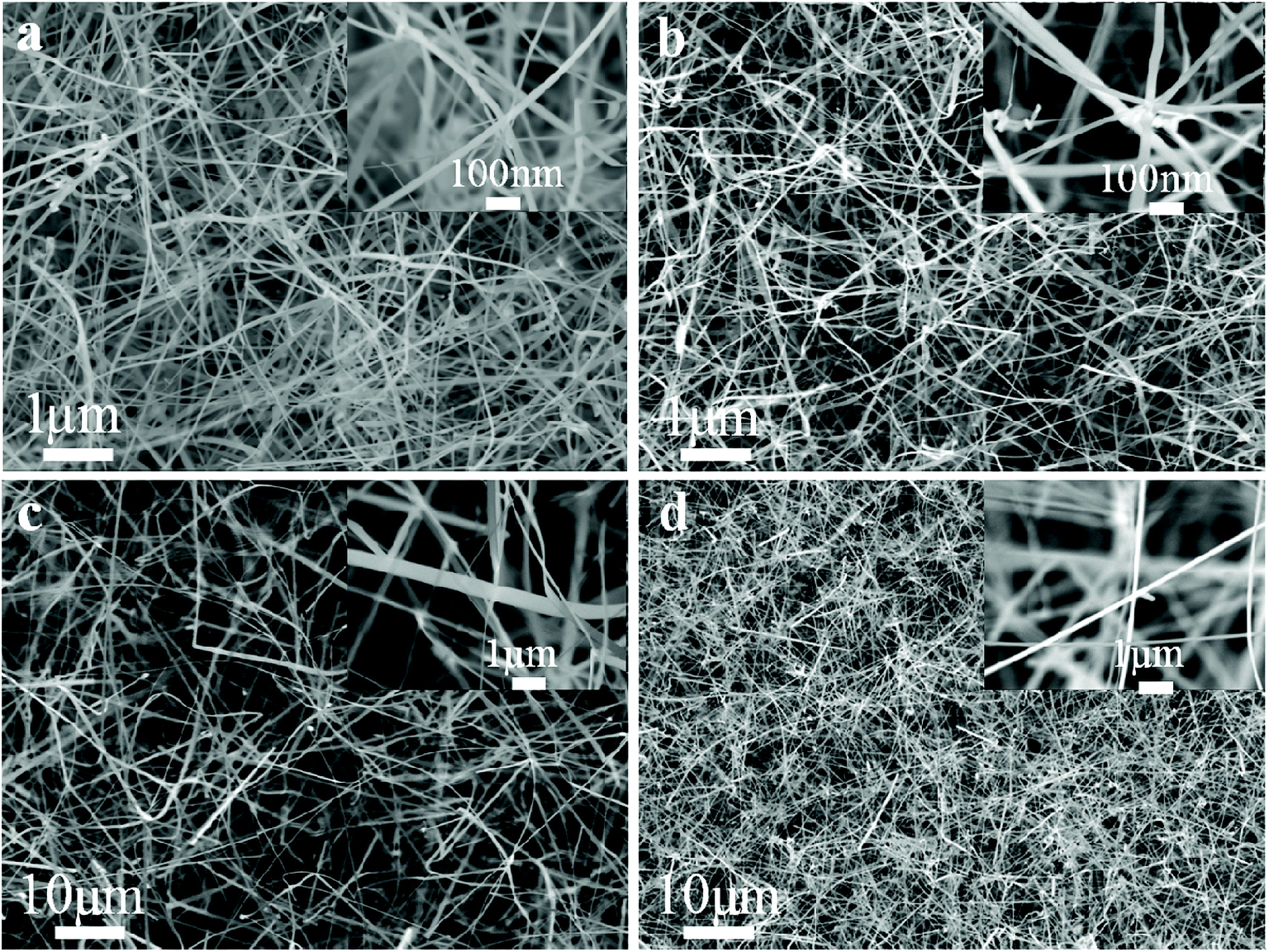 | ||
| Fig. 1 SEM images of the as-grown Zn2GeO4 NW networks grown under different pressures at 960 °C for 15 min, the insets show the high magnification SEM images. (a) 0.5 kPa; (b) 1 kPa; (c) 2 kPa; (d) 5 kPa. The insets show the enlarged SEM images of the respective samples. | ||
The effect of growth pressure on the product quality and purity was investigated by XRD technique, as shown in Fig. 2. As seen in Fig. 2a and b, when the growth pressure are 0.5 kPa and 1 kPa, the diffraction peak positions are in good agreement with the rhombohedral crystal of Zn2GeO4 phase (JCPDS card no. 11-0687). However, once the growth pressure is higher than 2 kPa, other diffraction peaks would appear and could be indexed to the diffraction peaks of ZnO (JCPDS card no. 79-0206), suggesting that ZnO is easier to grow along with Zn2GeO4 at higher pressure. This also suggests that the pure Zn2GeO4 NWs could only be obtained at a relatively lower growth pressure.
 | ||
| Fig. 2 XRD patterns of Zn2GeO4 NWs grown at different pressures. (a) 0.5 kPa; (b) 1 kPa; (c) 2 kPa; and (d) 5 kPa. | ||
Fine structures of individual Zn2GeO4 nanowires were then characterized using HRTEM. The low magnification TEM images of Zn2GeO4 NWs synthesized under pressure of 1 kPa are shown in Fig. 3a. The corresponding inserts give HRTEM images recorded along the [1![[1 with combining macron]](https://www.rsc.org/images/entities/char_0031_0304.gif) 0] zone axis. Specifically, the measured lattice distances was calculated to be about 0.71 nm and 0.31 nm which can be assigned to separations of the adjacent (110) and (113) planes, respectively. From the selected area electron diffraction (SAED) pattern of inset (a), it can be deduced that the preferred growth direction of a single nanowire is along the [001] direction.15 Combined the SAED and the high-resolution TEM (HRTEM) data, the formation of single crystalline nanowire could be confirmed readily. Simultaneously, the HRTEM also documented the high single-crystal quality of the samples, no defects were seen. It is obviously the excellent quality and high aspect ratios make the as-synthesized Zn2GeO4 nanowires become promising candidates for optoelectronic devices.
0] zone axis. Specifically, the measured lattice distances was calculated to be about 0.71 nm and 0.31 nm which can be assigned to separations of the adjacent (110) and (113) planes, respectively. From the selected area electron diffraction (SAED) pattern of inset (a), it can be deduced that the preferred growth direction of a single nanowire is along the [001] direction.15 Combined the SAED and the high-resolution TEM (HRTEM) data, the formation of single crystalline nanowire could be confirmed readily. Simultaneously, the HRTEM also documented the high single-crystal quality of the samples, no defects were seen. It is obviously the excellent quality and high aspect ratios make the as-synthesized Zn2GeO4 nanowires become promising candidates for optoelectronic devices.
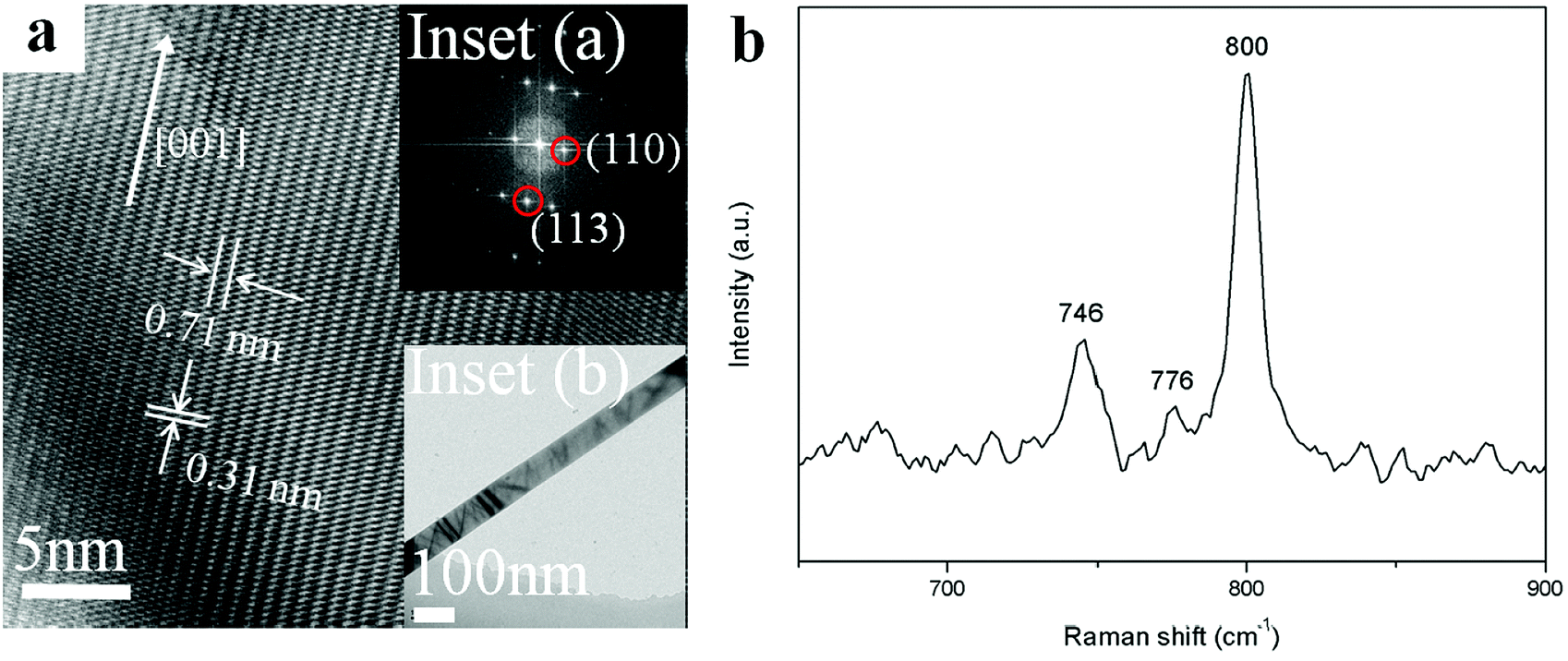 | ||
| Fig. 3 (a) HRTEM image of single Zn2GeO4 NWs grown at pressure of 1 kPa. Inset (a) is the corresponding SAED pattern, indicating that the growth direction of nanowire is [001]. Inset (b) shows the low magnification TEM image. (b) Raman spectrum of the Zn2GeO4 NWs grown at pressure of 1 kPa. | ||
Fig. 3b shows the local atomic structure of the Zn2GeO4 nanowires which was further investigated by Raman spectroscopy. The most prominent peak around 800 cm−1 which corresponds to the stretching vibration of GeO4 tetrahedra could be observed from the plot. The peaks at 746 and 776 cm−1 could be attributed to the symmetric and asymmetric stretching vibrations of Ge–O–Zn bonds, respectively.28,29 According to the previous report, the peak around 754 cm−1 was usually associated with oxygen defects in Zn2GeO4.30 However, it is visible this peak was not detectable in as-synthesized nanowires, indicating that there are negligible oxygen defects in the present Zn2GeO4 nanowires. It also suggested a high-quality crystal structure of the final products.
Fig. 4a shows the absorption spectrum of Zn2GeO4 nanowires on quartz substrate. The absorption peak of the nanowires can be seen clearly, and the peak position of the Zn2GeO4 nanowires locates at about 243 nm, indicating that the incorporation of germanium oxide makes the absorption spectrum of shift to deep ultraviolet. This observation reveals that the Zn2GeO4 NWs exhibit high wavelength selectivity in the UV-C region, as compared with the binary oxides, such as ZnO and SnO2.30–35 The bandgap of the Zn2GeO4 nanowires could also been obtained by fitting the absorbance with respect to the photon energy, as shown in Fig. 4b. The bandgap obtained from Tauc plot is 4.84 eV, which is in good agreement with the reported results.30
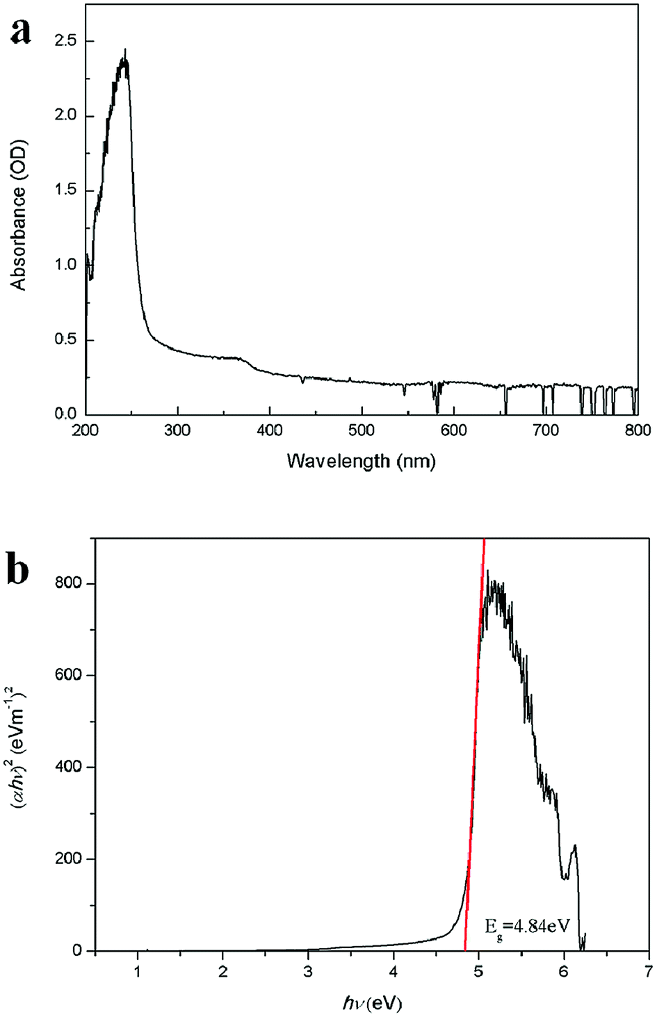 | ||
| Fig. 4 (a) The absorption spectrum of Zn2GeO4 NWs. (b) Tauc's plot of (αhν)2 as a function of photon energy hν for Zn2GeO4 NWs. | ||
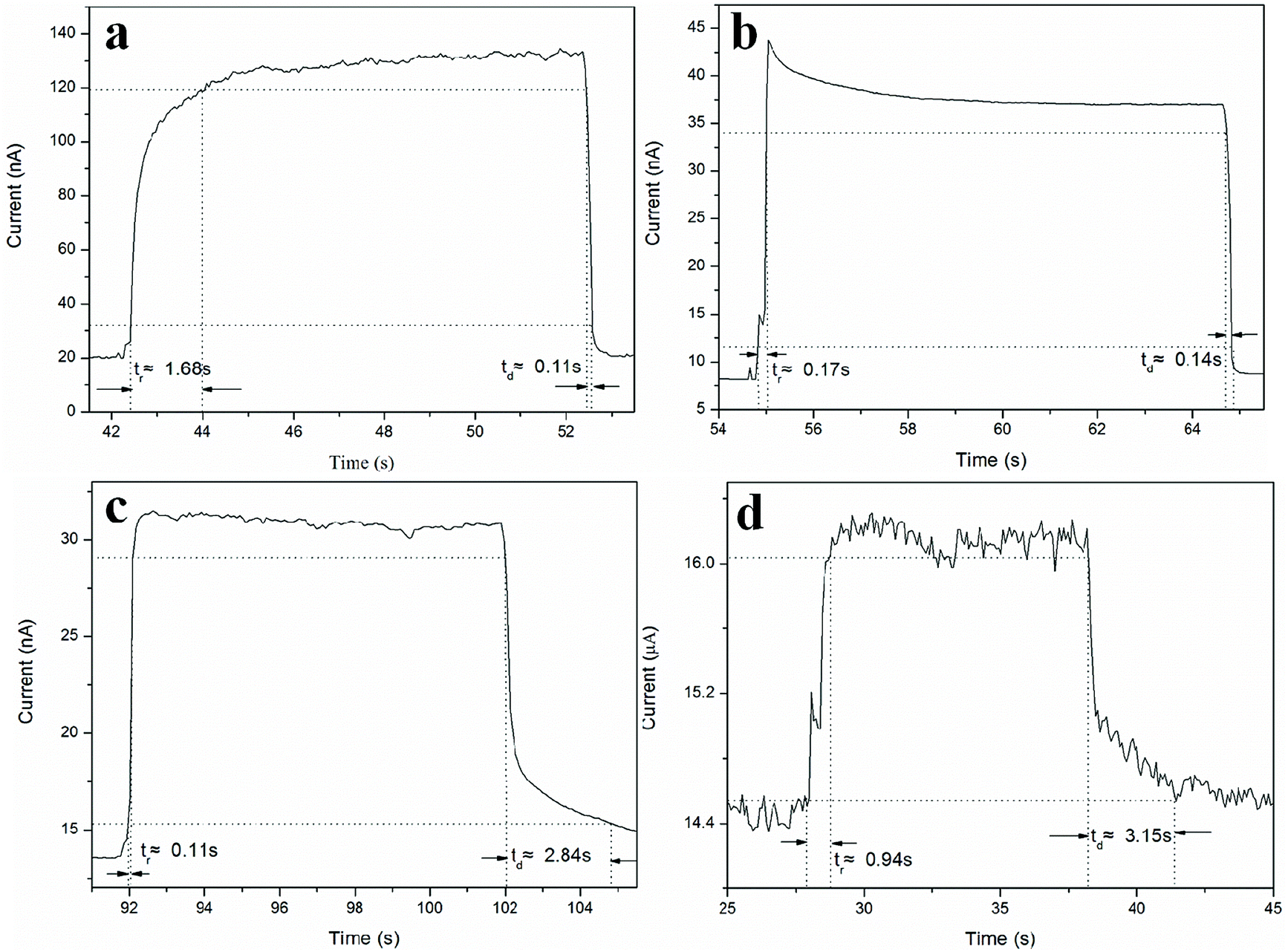
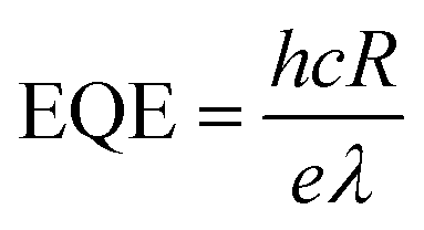
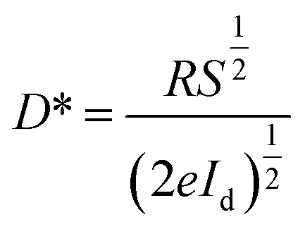
To examine the response time of the Zn2GeO4 nanowires UV photodetector, a LED lamp with wavelength of 256 nm and energy density of 1.76 mW cm−2 was used as a light source. The time-dependent photocurrent at 8 V bias with multiple UV on/off cycles was measured at room temperature, in which both the “on” and “off” times of the UV illumination were 20 s. It is well-known that oxygen molecules absorbed on the surface of Zn2GeO4 act as electron acceptors to form O2− by capturing free electrons from the surface in dark, creating a low conductive depletion layer near the Zn2GeO4 surface.1,2,27,28 Upon UV illumination, the photogenerated holes in Zn2GeO4 migrate to the surface and neutralize the O2− ions, while the unpaired electrons significantly enhance the conductivity of the sample. The photoelectric characteristic images of Zn2GeO4 nanowire networks under different pressures (0.5–5 kPa) with a period of 20 s are shown in Fig. 5. As shown in Fig. 5a, upon UV illumination, the current would first rapidly ramp to 130 nA from the dark current, then it increases tardily to 140 nA, and as UV illumination is off, the current would promptly fall to the original level. From Fig. 5b, it can be seen that current dramatically expands from the dark current to 44 nA, which is associated to UV illumination, and then it gradually goes down to around 37 nA, and when UV illumination is off, the current would swiftly decline to around the original level. It is evident that upon UV illumination, the current would first quickly change to 31 nA from the dark current, and then decrease gently to 30 nA, and as UV illumination is off, the current would first speedily descend to 17 nA and then slowly decay to around the dark current from Fig. 5c. As shown in Fig. 5d, upon UV illumination, the current would first drastically go up to 16 nA from the dark current, followed by a slow rise to 16.5 nA, and as UV illumination is off, the current would first sharply reduce to 15 nA and then drop to around the original level by inches. It is clear that by switching on and off the electron beam, the devices run with good repeatability with fast response (<1 s).
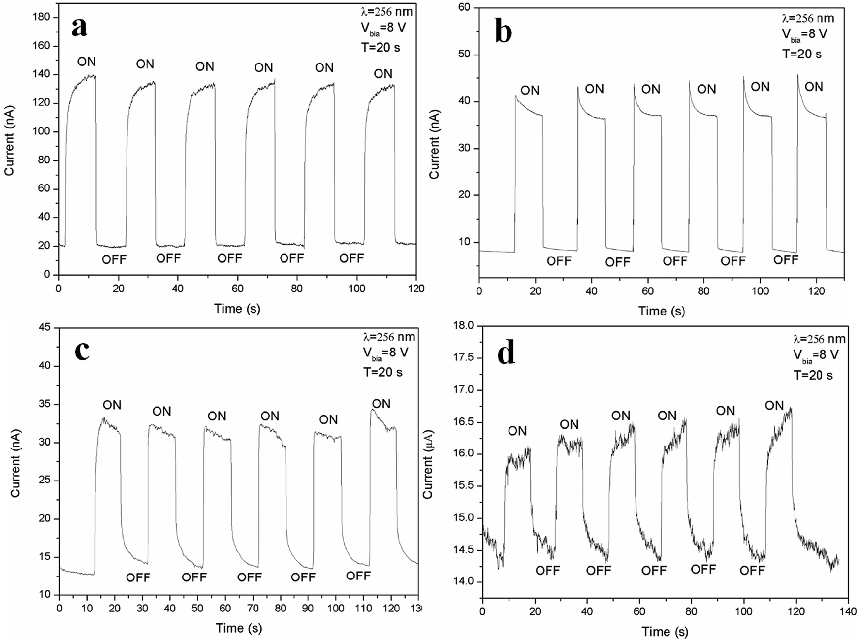 | ||
| Fig. 5 Time-resolved rise and decay of photocurrent with UV illumination on and off periods of 20 s under a bias of 8 V of Zn2GeO4 NW networks grown under pressures of 0.5 kPa (a), 1 kPa (b), 2 kPa (c), and 5 kPa (d). | ||
It is obvious that the device (under a bias of 8 V) shows a good stability, as well as fast rise and decay times, as illustrated in Fig. 6. If we define tr and td as the times required for the current to increase from 10% to 90% of the peak value or vice versa,15 then the response and recovery time of the photodetectors prepared from Zn2GeO4 NWs grown at 0.5 kPa can be calculated to be 1.68 s and 0.11 s, respectively. From the curve, it can be seen that the typical response time of the Zn2GeO4 NW network UV PD with nanowires synthesized under 1 kPa is about 0.17 s and it has a steep falling edge, giving a recovery time of 0.14 s. The measured tr and td of the Zn2GeO4 NW network UV PD made of NWs grown at 2 kPa can be deduced to be 0.11 s and 2.48 s, respectively. On the contrary, the device fabricated from Zn2GeO4 NW synthesized under 5 kPa has the response and recovery time of tr = 0.94 s and td = 3.15 s respectively.
 | ||
| Fig. 6 Enlarged view of typical rise and decay curves for Zn2GeO4 NW network PD synthesized at different pressures with and without UV illumination. (a) 0.5 kPa; (b) 1 kPa; (c) 2 kPa; and (d) 5 kPa. | ||
It is found that the rise process (0.17 s) of the Zn2GeO4 NW network UV PD with nanowires synthesized under 1 kPa is much faster than that of Zn2GeO4 NW PD obtained from nanowires grown at 0.5 kPa (1.68 s) and 5 kPa (0.94 s), while the rise stage of Zn2GeO4 NW network PD prepared from NWs produced at 1 kPa is also comparable with that of the device with nanowires grown at 2 kPa (0.11 s).31 Likewise, the resetting process of the PDs with NWs grown 1 kPa (0.14 s) is much faster than the devices corresponding to 2 kPa (2.84 s) and 5 kPa (3.15 s), while the decay stage of the Zn2GeO4 NW PD produced at 1 kPa is also comparable with that of NW device grown at 0.5 kPa (0.11 s). This is much better than most reported PDs based on Zn2GeO4 nanostructures, as shown in Table 1.34
| Photodetectors | Bias (V) | UV light (nm) and power density (mW cm−2) | Rise time (s) | Decay time (s) | Ref. |
|---|---|---|---|---|---|
| Zn2GeO4 NW | 3 | λ = 254, P = / | 0.6 | 1.5 | 9 |
| Zn2GeO4 NW mats | 20 | λ = 254, P = 0.2 | 0.3 | 0.2 | 30 |
| Zn2GeO4 NW | 8 | λ = 245, P = 0.05 | 12 | 0.6 | 37 |
| In2Ge2O7 NW mats | 20 | λ = 254, P = 0.85 | 15 | <1 | 38 |
| Zn2GeO4 NW | 3 | λ = 254, P = 0.85 | 3 | <1 | 38 |
| ZnGa2O4 NW | 5 | λ = 350, P = 0.53 | 15 | 10 | 39 |
| Zn2GeO4 NW networks | 8 | λ = 256, P = 1.76 | 0.17 | 0.14 | This work |
To determine the other aspects of sensing performance, the responsivity (R), external quantum efficiency (EQE) and detectivity (D*) corresponding to the detectors of different growth pressures were calculated. The responsivity of the Zn2GeO4 nanowires UV photodetectors is defined as the ratio of the response current to the illumination power on photodetector as given by:15,33,40
 | (1) |
 | (2) |
 | (3) |
| Photodetectors of different growth pressures | Responsivity (R) | External quantum efficiency (EQE) | Detectivity (D*) |
|---|---|---|---|
| 0.5 kPa | 1.7 × 10⁻³ A W−1 | 0.82% | 4.25 × 10⁹ jones |
| 1 kPa | 5.11 × 10⁻⁴ A W−1 | 0.25% | 2.03 × 10⁹ jones |
| 2 kPa | 2.98 × 10⁻⁴ A W−1 | 0.15% | 9.22 × 10⁸ jones |
| 5 kPa | 4.26 × 10⁻⁵ A W−1 | 0.02% | 1.27 × 10⁸ jones |
The entanglement between Zn2GeO4 NWs is beneficial to response speed through the mechanism of Schottky barriers at the junctions between the interconnected Zn2GeO4 NWs. On the other hand, the entanglement in Zn2GeO4 NWs usually formed in high density Zn2GeO4 NWs at the cost of photo-to-dark current ratio.34 There are two main factors for high dark current. First, only very few Zn2GeO4 NWs on the top of Zn2GeO4 NW networks could absorb and be excited by UV illumination. Second, there would form a Zn2GeO4 film on the substrate as the reaction proceeds and contribute to the high dark current.34 While the structure of interconnection of Zn2GeO4 NWs has fast response time, the electrical signal of the material is weak, which affects the value of the responsivity, external quantum efficiency and detectivity of photodetectors.
Fig. 7 shows the schematic diagram depicting the carrier generation and transportation processes in the Zn2GeO4 NW network devices. It is well accepted that the processes of oxygen adsorption and desorption corresponding to the UV response and recovery are associated with the photogeneration of free carriers.30,35,36,38–43 In ambient conditions, oxygen molecules would adsorb on the surface of Zn2GeO4 NW to form O2− by capturing free electrons from NW surface through O2 (g) + e− → O2− (ad), creating a lowly conductive surface depletion layer, as shown in Fig. 6a. Under the UV irradiation, the electron–hole pairs are generated by directly exciting electrons from the valence band to conduction band, which increase carrier density significantly in the NWs. The photon-generated holes would migrate to the surface and discharge the adsorbed oxygen ions through O2− (ad) + h+ → O2 (g), resulting in a reduction in the depletion barrier thickness. The increase in carrier concentration and oxygen desorption caused by hole-trapping process contribute to an apparent enhancement of conductance in the NW networks.30–34 As the UV illumination is turned off, holes recombine with electrons, meanwhile oxygen re-absorb on Zn2GeO4 NW surface by capturing electrons returning the device to initial low conductivity state.
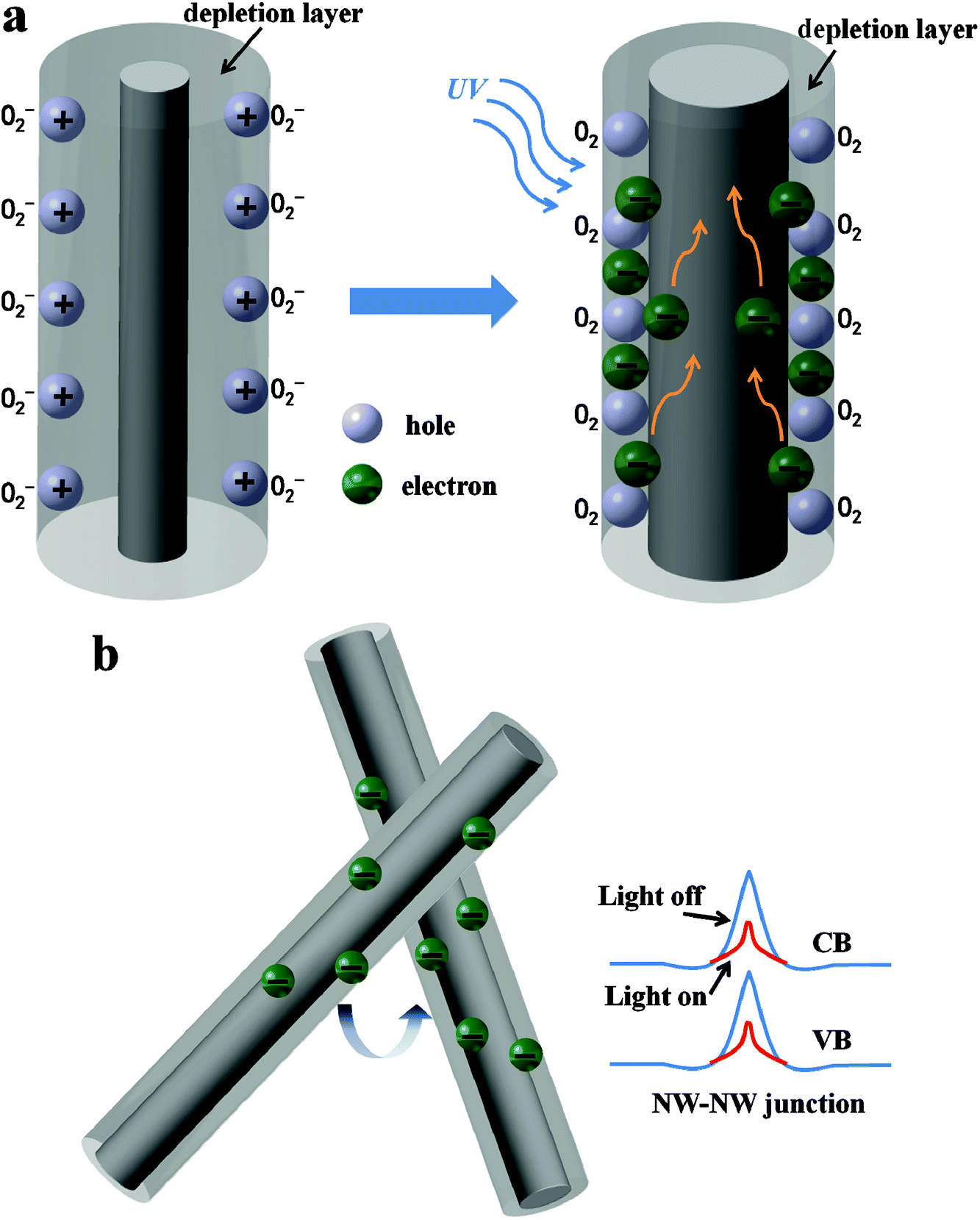 | ||
| Fig. 7 Schematic of the carrier generation and NW–NW junction barrier for electron transfer in the network device. (a) Carrier generation in a single Zn2GeO4 NW; (b) carrier generation and transport in Zn2GeO4 NW. | ||
In addition to the same photoconductive mechanism of photogeneration of free carriers, compared with single NW PD, network devices have another unique conducting mechanism that is the transport of carriers across the interface between neighboring NWs. As Fig. 6b illustrates, the resistance of two crossed NWs was dominated by the NW–NW junction barrier, rather than the resistances of the NW themselves.44,45 In the Zn2GeO4 NW PD, electrons must overcome the NW–NW junction barrier when tunneling from one NW to another as shown in Fig. 6b. It is reported that the electron-transfer barrier originates from the surface depletion layers and the depletion layer would be narrowed upon UV illumination on account of the increase of carrier density, which is equivalent to a lowering of the effective barrier height.30–34 It makes electrons more likely to transport in the networks upon UV irradiation and hence resulting in the increment of current, as illustrated in Fig. 4.
Compared with the previously reported devices with slow response and recovery time,36,39,43–48 the fast recovery time 0.14 s for our Zn2GeO4 NW photodetectors can be attributed to the NW–NW junction barrier dominated conductance. Typically, because it needs a long time for the oxygen diffusion and re-adsorption to deplete the NW channel, the NW conductance is still higher than its initial value within a short period upon turning off the UV light.30,43,46–48 For the NW network structures, the depletion barrier can be analogous to two back-to-back Schottky barriers, as the UV light is switched on, which is much lower in the effective barrier height due to the greatly incremental carrier density. The dominate role of the junction barrier would cause a current decay almost approaching its initial value within a short period for our devices. The modulation of barrier height induced by irradiation is typically much faster than the oxygen diffusion process on the order of several minutes or hours. This paper demonstrates that the response and recovery time can be enhanced by using NW networks with NW–NW barrier dominated conductance. It can be seen that apart from no requirement for intense and expensive lithography processes, the simple and feasible preparation technics also allows potential large-scale device fabrication.
4. Conclusion
In conclusion, we have prepared wide-bandgap Zn2GeO4 NW networks by CVD at lower pressures (0.5–5 kPa) and investigated their corresponding DUV detection performance. We found that the pure Zn2GeO4 NWs could be obtained at 1 kPa or lower pressure. The Zn2GeO4 NW networks produced under 1 kPa exhibited efficient response for UV photodetection. The network devices showed response and recovery time of 0.17 s and 0.14 s, respectively, which can be attributed to the NW–NW junction barrier dominant conductance. The large bandgap 4.84 eV makes the NW materials promising for UV-C detection with high wavelength selectivity. The network-enabled fast response and recovery time as well as facile fabrication processes may also be extended to other ternary metal oxide nanomaterials.Conflicts of interest
There are no conflicts to declare.Acknowledgements
This work was supported by the Chongqing Research Program of Basic Research and Frontier Technology (No. cstc2017jcyjBX0030), the National Natural Science Foundation of China (No. 61605207, No. 11875210 and 11805169), the Fundamental Research Funds for the Central Universities of China, the 111 project (B13015) to Harbin Engineering University, the Natural Science Foundation of Heilongjiang Province, China (Grant No. A2018004), and the Opened Fund of the Key Lab of In-fiber Integrated Optics, Ministry Education of China, the scientific and technological project of Henan province (No. 182102210419), Special Funds for Developing Local Science and Technology from Central Government under Award No. Y82Z230H10.References
- H. Kind, H. Q. Yan, B. Messer, M. Law and P. D. Yang, Adv. Mater., 2002, 14, 158–160 CrossRef CAS.
- Z. R. Dai, Z. W. Pan and Z. L. Wang, Adv. Funct. Mater., 2003, 13, 9–24 CrossRef CAS.
- S. Xu, Y. Qin, C. Xu, Y. Wei, R. Yang and Z. L. Wang, Nat. Nanotechnol., 2010, 5, 366–373 CrossRef CAS.
- J. Bao, M. A. Zimmler, F. Capasso, X. Wang and Z. Ren, Nano Lett., 2006, 6, 1719–1722 CrossRef CAS PubMed.
- S. J. Chang, T. J. Hsueh, I. C. Chen and B. R. Huang, Nanotechnology, 2008, 19, 175502–175506 CrossRef PubMed.
- J. Zhou, Y. Gu, Y. Hu, W. Mai, P. H. Yeh, G. Bao, A. K. Sood, D. L. Polla and Z. L. Wang, Appl. Phys. Lett., 2009, 94, 191103 CrossRef PubMed.
- C. Y. Hsieh, M. L. Lu, J. Y. Chen, Y. T. Chen, Y. F. Chen, W. Y. Shih and W. H. Shih, Nanotechnology, 2012, 23, 355201–355205 CrossRef PubMed.
- S. Liang, H. Sheng, Y. Liu, Z. Huo, Y. Lu and H. Shen, J. Cryst. Growth, 2001, 225, 110–113 CrossRef CAS.
- C. H. Liao, C. W. Huang, J. Y. Chen, C. H. Chiu, T. C. Tsai, K. C. Lu, M. Y. Lu and W. W. Wu, J. Phys. Chem. C, 2014, 118, 8194–8199 CrossRef CAS.
- Q. Zhang, J. S. Jie, S. L. Diao, Z. V. Shao, Q. Zhang, L. Wang, W. Deng, W. D. Hu, H. Xia, X. D. Yuan and S. T. Lee, ACS Nano, 2015, 9, 1561–1570 CrossRef CAS PubMed.
- R. J. Zou, Z. Y. Zhang, Q. Liu, J. Q. Hu, L. W. Sang, M. Y. Liao and W. J. Zhang, Small, 2014, 10, 1848–1856 CrossRef CAS PubMed.
- X. Fang, Y. Bando, M. Liao, T. Zhai, U. K. Gautam, L. Li, Y. Koide and D. Golberg, Adv. Funct. Mater., 2010, 20, 500–508 CrossRef CAS.
- Y. Li, T. Tokizono, M. Liao, M. Zhong, Y. Koide, I. Yamada and J. J. Delaunay, Adv. Funct. Mater., 2010, 20, 3972–3978 CrossRef CAS.
- T. Zhai, L. Li, X. Wang, X. Fang, Y. Bando and D. Golberg, Adv. Funct. Mater., 2010, 20, 4233–4248 CrossRef CAS.
- X. Zhou, Q. Zhang, L. Gan, X. Li, H. Li, Y. Zhang, D. Golberg and T. Zhai, Adv. Funct. Mater., 2016, 26, 704–712 CrossRef CAS.
- Z. Zhang, Q. L. Liao, Y. H. Yu, X. D. Wang and Y. Zhang, Nano Energy, 2014, 9, 237–244 CrossRef CAS.
- X. K. Zhang, Q. L. Liao, S. Liu, Z. Kang, Z. Zhang, J. L. Du, F. Li, S. H. Zhang, J. K. Xiao, B. S. Liu, Y. Ou, X. Z. Liu, L. Gu and Y. Zhang, Nat. Commun., 2017, 8, 15881 CrossRef CAS PubMed.
- J. Z. Song and H. B. Zeng, Angew. Chem., Int. Ed., 2015, 54, 9760–9774 CrossRef CAS PubMed.
- S. Majety, J. Li, X. K. Cao, R. Dahal, B. N. Pantha, J. Y. Lin and H. X. Jiang, Appl. Phys. Lett., 2012, 100, 061121 CrossRef.
- S. Ohmagari and T. Yoshitake, Appl. Phys. Express, 2012, 5, 5202 Search PubMed.
- J. Zhou, Y. Gu, Y. Hu, W. Mai, P. H. Yeh, G. Bao, A. K. Sood, D. L. Polla and Z. L. Wang, Appl. Phys. Lett., 2009, 94, 191103 CrossRef PubMed.
- C. Y. Hsieh, M. L. Lu, J. Y. Chen, Y. T. Chen, Y. F. Chen, W. Y. Shih and W. H. Shih, Nanotechnology, 2012, 23, 355201–355205 CrossRef PubMed.
- S. Mehrabani, P. Kwong, M. Gupta and A. M. Armani, Appl. Phys. Lett., 2013, 102, 241101 CrossRef.
- X. Pan, X. Liu, A. Bermak and Z. Fan, ACS Nano, 2013, 7, 9318–9324 CrossRef CAS PubMed.
- J. Z. Song, J. H. Li, J. Y. Xu and H. B. Zeng, Nano Lett., 2014, 14, 6298–6305 CrossRef CAS PubMed.
- Y. Zhang, Y. Yang, Y. S. Gua, X. Q. Yan, Q. L. Liao, P. F. Li, Z. Zhang and Z. Z. Wang, Nano Energy, 2015, 14, 30–48 CrossRef CAS.
- L. Xu, X. Li, Z. Zhan, L. Wang, S. Feng, X. Chai, W. Lu, J. Shen, Z. Weng and J. Sun, ACS Appl. Mater. Interfaces, 2015, 7, 20264–20271 CrossRef CAS PubMed.
- X. Q. Liao, X. Q. Yan, P. Lin, S. G. Lu, Y. Tian and Y. Zhang, ACS Appl. Mater. Interfaces, 2015, 7, 1602–1607 CrossRef CAS PubMed.
- X. Lang, A. Hirata, T. Fujita and M. Chen, Nat. Nanotechnol., 2011, 6, 232–236 CrossRef CAS PubMed.
- C. Yan, N. Singh and P. S. Lee, Appl. Phys. Lett., 2010, 96, 053108 CrossRef.
- J. H. Song, X. D. Wang, E. Riedo and Z. L. Wang, J. Phys. Chem. B, 2005, 109, 9869–9872 CrossRef CAS PubMed.
- E. S. Babu, S. J. Kim, J. H. Song and S. K. Hong, Chem. Phys. Lett., 2016, 658, 182–187 CrossRef CAS.
- Z. Zhan, L. Xu, J. An, H. Du, Z. Weng and W. Lu, Adv. Eng. Mater., 2017, 19, 1700101 CrossRef.
- L. Li, H. Jiang, X. Han, Z. Zhan, H. Du, W. Lu, Z. Li, Z. Tao and Y. Fan, Ceram. Int., 2017, 43, 15978–15985 CrossRef CAS.
- Z. Q. Liu, D. H. Zhang, S. Han, C. Li, T. Tang, W. Jin, X. L. Liu, B. Lei and C. W. Zhou, Adv. Mater., 2003, 15, 1754–1757 CrossRef CAS.
- C. Soci, A. Zhang, B. Xiang, S. A. Dayeh, D. P. R. Aplin, J. Park, X. Y. Bao, Y. H. Lo and D. Wang, Nano Lett., 2007, 7, 1003–1009 CrossRef CAS PubMed.
- C. Li, Y. Bando, M. Y. Liao, Y. Koide and D. Golberg, Appl. Phys. Lett., 2010, 97, 161102 CrossRef.
- Z. Liu, H. T. Huang, B. Liang, X. F. Wang, Z. R. Wang, D. Chen and G. Z. Shen, Opt. Express, 2012, 20, 2982–2991 CrossRef CAS PubMed.
- Z. Lou, L. D. Li and G. Z. Shen, Nano Res., 2015, 8, 2162–2169 CrossRef CAS.
- S. L. Wang, Y. S. Zou, Q. S. Shan, J. Xue, Y. H. Dong, Y. Gu and J. Z. Song, RSC Adv., 2018, 8, 33666–33673 RSC.
- H. Kind, H. Q. Yan, B. Messer, M. Law and P. D. Yang, Adv. Mater., 2002, 14, 158–160 CrossRef CAS.
- Y. H. Dong, Y. Gu, Y. S. Zou, J. Z. Song, L. M. Xu, J. H. Li, J. Xue, X. M. Li and H. B. Zeng, Small, 2016, 12, 5622–5632 CrossRef CAS PubMed.
- J. Zhou, Y. D. Gu, Y. F. Hu, W. J. Mai, P. H. Yeh, G. Bao, A. K. Sood, D. L. Polla and Z. L. Wang, Appl. Phys. Lett., 2009, 94, 191103 CrossRef PubMed.
- X. F. Duan, Y. Huang, Y. Cui, J. F. Wang and C. M. Lieber, Nature, 2001, 409, 66–69 CrossRef CAS PubMed.
- Y. Cui and C. M. Lieber, Science, 2001, 291, 851–853 CrossRef CAS PubMed.
- A. Umar, B. K. Kim, J. J. Kim and Y. B. Hahn, Nanotechnology, 2007, 18, 175606 CrossRef.
- S. W. Lee, M. C. Jeong, J. M. Myoung, G. S. Chae and I. J. Chung, Appl. Phys. Lett., 2007, 90, 133115 CrossRef.
- G. Lubberts, B. C. Burkey, H. K. Bucher and E. L. Wolf, J. Appl. Phys., 1973, 45, 92–95 Search PubMed.
| This journal is © The Royal Society of Chemistry 2019 |