
 Open Access Article
 This Open Access Article is licensed under a
 Creative Commons Attribution 3.0 Unported Licence
New aspects of improving the performance of WO3 thin films for photoelectrochemical water splitting by tuning the ultrathin depletion region†
Jiajie Cen a,
Qiyuan Wua,
Danhua Yanab,
Wenrui Zhangb,
Yue Zhaoc,
Xiao Tongb,
Mingzhao Liu*b and
Alexander Orlov*a
a,
Qiyuan Wua,
Danhua Yanab,
Wenrui Zhangb,
Yue Zhaoc,
Xiao Tongb,
Mingzhao Liu*b and
Alexander Orlov*a
aDepartment of Materials and Science Engineering, Stony Brook University, Stony Brook, New York, 11794, USA. E-mail: alexander.orlov@stonybrook.edu
bCenter for Functional Nanomaterials, Brookhaven National Laboratory, Upton, New York, 11973, USA. E-mail: mzliu@bnl.gov
cDepartment of Chemistry, Stony Brook University, Stony Brook, New York, 11794, USA
First published on 8th January 2019
Abstract
In this work, we explored a facile, scalable and effective method for substantially enhancing photocurrent and incident-photon-to-current efficiency of WO3 thin-film photoanodes by a mild reduction treatment under low oxygen pressure. Experimental data from photoelectrochemical and electrochemical impedance spectroscopies have shown that such treatment can increase the charge carrier density on WO3 photoanode surfaces resulting in improvements in hole collection efficiency and reduction in charge recombination. Despite a much thinner layer of WO3 (about 500 nm) compared to those in other published studies, the electrodes exhibited an ultra-high photocurrent density of 1.81 mA cm−2 at 1.23 V vs. RHE. This current density is one of the highest ones among WO3-based photoanodes described in literature. The proposed surface modulation approach offers an effective and scalable method to prepare high-performance thin film photoanodes for photoelectrochemical water splitting.
1. Introduction
Water splitting in photoelectrochemical (PEC) cells is potentially the most promising method for converting solar energy into chemical energy. Tungsten trioxide (WO3), which is an n-type semiconductor, is one of the most promising candidate materials for PEC water oxidation.1 This semiconductor has an indirect band gap of 2.5–2.8 eV while being among only a few visible-light-responsive photocatalysts that exhibit outstanding stability in acidic electrolytes (pH ≤ 4). In contrast, other visible-light activated photoanode materials, such as BiVO4 and α-Fe2O3, are less stable under the same acidic conditions. This is important as photoanodes with significant stability in acidic environments (e.g. WO3) could be utilized in acidic water electrolyzers based on polymer electrolyte membranes, which overcomes many of the disadvantages of the conventional alkaline electrolyzers.2 The disadvantages of WO3 based anodes stem from their indirect band gap. As a result, WO3 exhibits a weak light absorption in visible range (α = 104 to 105 cm−1), which is about one order of magnitude lower than that of other visible light photocatalysts, such as Fe2O3 and BiVO4. This disadvantage can be potentially offset by having a relatively long (∼500 nm) hole diffusion length in the WO3 materials, thereby conceivably offering a more efficient carrier delivery from bulk to depletion region. The overall result of a combination of unfavorable weak light adsorption and favorable diffusion length is that most of the incident photons interacting with WO3 photoanodes are absorbed beyond the depletion region, resulting in an insufficient charge carrier separation despite the carrier's high mobility.In the past WO3 photoanodes were usually prepared as thick films (typically a few micrometers in thickness) to overcome the weak visible light absorption.3–13 Other attempts to improve absorption included tuning the illuminated surface area by introducing surface microstructures,6,14–17 which might not be a practical and scalable way forward. In addition to tuning light absorption on photoanode, another strategy to improve the photocurrent is to overcome the kinetic limitation in O2 evolution by introducing modification on the photoanode surface with appropriate co-catalysts. Among a few examples of oxygen evolution catalysts deposited on WO3, Bi2S3, Sb2S3, CoOx, FeOOH, and IrO2 are the most promising ones, with only IrO2 offering good stability in acidic electrolyte.18–24 While exhibiting an improved oxygen evolution performance, these catalysts also reduce the photon flux reaching WO3 due to their non-transparent nature.25,26 Therefore, the potential improvements for oxygen evolution by surface-decorated co-catalyst is offset by reduced light absorption. In addition to modifying surfaces, adding catalysts to electrolytes was also explored. It was found that both phosphotungstate and phosphomolybdate improved the WO3 photoanode performance.27 However, despite some success in using the above mentioned strategies, it is still a challenge to develop highly efficient visible light absorbing photoanodes with very transparent oxygen evolution catalysts that can also offer thermodynamic stability in acidic electrolytes.18
In order to move this field further, it is important to critically evaluate the mechanistic aspects of the current electrode design strategies. In our work, we address a specific challenge of improving the PEC activity of unmodified WO3 electrode without creating a thick film electrode geometry, which causes photon adsorption beyond the carrier diffusion region. Introduction of oxygen vacancies to the surface of semiconductors can be one promising strategy to improve WO3 photocatalytic efficiency while keeping relatively thin thickness.28 Oxygen vacancies typically act as donor defects for n-type oxides, where they exert a significant influence on space charge region (SCR) and charge recombination.11–13,29 In addition, dual oxygen and tungsten vacancies have proven to significantly enhance the hole transfer efficiency at semiconductor electrolyte interface (SEI).4 Therefore, modulating the functions of vacancies at the surface of semiconductors using a finely controlled method can be a potentially promising way forward to design high performance thin film PEC electrodes. The novel aspects of this study are in developing sophisticated performance tuning of WO3 electrodes by simultaneous fine adjustment of both oxygen vacancies and thickness of the oxide layer, while maintaining a good crystallinity of the sample. Here we introduce a simple surface reduction method that can significantly enhance the performance of bare WO3 thin film photoanodes, which are only 500 nm thick. These photoanodes showed a performance similar to that of other literature described WO3 photoanodes with few micrometers in thickness. Our results demonstrate that a sophisticated control of the electrode surfaces reduction is necessary to further optimize water oxidation activity of WO3 photoanodes.
2. Results and discussion
Fabrication of the water splitting photoanodes was accomplished by depositing WO3 thin films on ITO glass substrates using pulsed laser deposition (PLD). The thicknesses of the WO3 thin films were controlled by the total number of laser pulses. The conditions of thin film deposition were optimized based on PEC measurements on as-deposited WO3 photoanodes (Fig. S2, ESI†). Following the PLD deposition, the film was annealed under decreased partial oxygen pressure (pO2) of 95 mTorr to achieve surface reduction (Fig. 2a). This approach was consistent with published strategy of adjusting WO3−x composition by tuning (pO2) during annealing. Samples reduced for 0, 200, 400, and 600 seconds under 95 mTorr of pO2 were labelled as R0 (pristine), R1, R2, and R3 respectively. The as-deposited pristine WO3 film exhibited an intrinsic optical absorption up to 450 nm (Fig. 1c), which according to the Tauc plot indicates an indirect band edge at 2.7 eV. The X-ray diffraction (XRD) patterns collected from the thin films were indexed as monoclinic WO3 (PCPDF# 72-1465), and the strongest diffraction signal consistently arose from the (002) plane, indicating it as the preferred domain orientation (Fig. S4b, ESI†). The Raman spectra (Fig. S4c, ESI†) show the most intense bands at 805 cm−1 and 715 cm−1 were assigned to O–W–O stretching vibrations, while the bands at 274 cm−1 and 332 cm−1 were assigned to O–W–O bending vibrations.30–33 The scanning electron microscopy (SEM) image (Fig. 1d) showed high uniformity of the WO3 thin film morphology. The cross-sectional SEM image of WO3 thin film sample prepared by 40k laser pulses (Fig. 1b), which included ITO bottom electrode, indicated that its thickness was about 500 nm. After the reduction treatment, no significant differences in UV-vis, XRD and Raman of the reduced samples were observed (Fig. S4, ESI†). The lattice spacing calculated from the high-resolution TEM (HRTEM) images (Fig. 4c and f) was 3.90 Å, corresponding to the distance between the (002) planes of a monoclinic WO3 phase.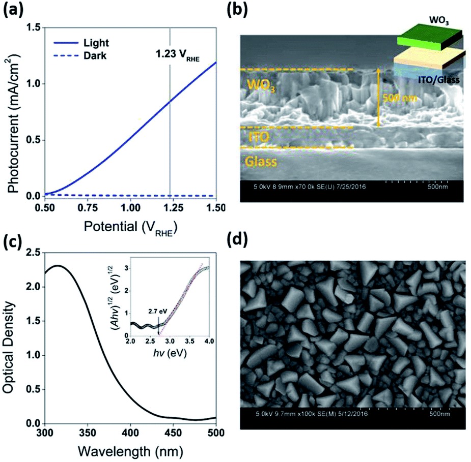 | ||
| Fig. 1 (a) Current density vs. potential under front-side AM 1.5 illumination for the as-prepared WO3 photoanodes (R0). The vertical line indicates the thermodynamic potential for oxygen evolution (1.23 VRHE). (b) Cross-sectional SEM image of WO3 thin film sample prepared by 40k laser pulses. (c) UV-vis spectrum of as-prepared WO3 photoanodes (R0) with Tauc plot inserted. (d) SEM image of as-prepared WO3 photoanodes (R0). | ||
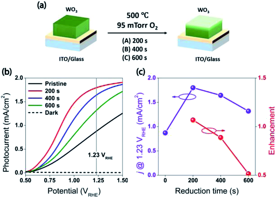 | ||
| Fig. 2 (a) The illustration of mild reduction treatment. (b) Current density vs. potential under front-side AM 1.5 illumination for the WO3 photoanodes, R0, R1, R2, and R3. The vertical line indicates the thermodynamic potential for oxygen evolution (1.23 VRHE). (c) The photocurrent of the WO3 photoanodes (R0, R1, R2, and R3) at 1.23 VRHE, and the relative enhancements for the reduced WO3 photoanodes (R1, R2, and R3). The characterization of the photoanodes were conducted in 0.5 M H2SO4 electrolyte. | ||
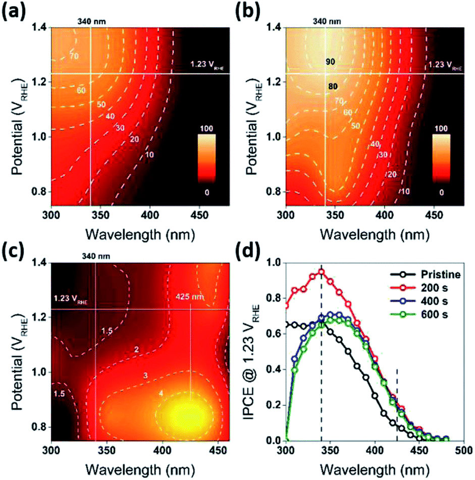 | ||
| Fig. 3 (a and b) Front-side (EE) IPCE as a function of excitation wavelength potential, for the R0 (Pristine) and R1 (reduced for 200 s) WO3 photoanodes. Both the panels share the same color scale. The dashed lines are contours for corresponding IPCE values in percentage. (c) The ratio of IPCE values for sample R1/R0. The dashed lines are contours for corresponding enhancement of IPCE values. The horizontal white lines indicate the thermodynamic potential for oxygen evolution (1.23 VRHE). (d) Front-side (EE) IPCE measurements for the WO3 photoanodes (R0, R1, R2, and R3), carried out at 1.23 VRHE. The characterization of the photoanodes were conducted in 0.5 M H2SO4 electrolyte. | ||
The water splitting properties of the WO3 thin film photoanodes were studied by photoelectrochemical methods. According to the current density–potential (J–E) curves, which were measured in a 0.5 M H2SO4 solution (pH = 0.3) under front-side (electrolyte–electrode side, EE) AM 1.5G illumination (Fig. 2b and c), all the WO3 photoelectrodes produced anodic photocurrents that were consistent with the n-type doping. The onset potentials of all photoanodes were approximately 0.50 VRHE. The sample treatment in reduced atmosphere significantly improved photocurrents (samples R1, R2 and R3)., The sample R1, which was annealed for 200 s, exhibited the largest photocurrent (1.80 mA cm−2 at 1.23 VRHE), which was 2 times higher than that of the pristine sample. Increasing annealing time to 400 and 600 s, resulted in photocurrent decrease for samples R2 and R3. Additional insights into the observed trends were provided by the incident-photon-to-current efficiency (IPCE) measurements. Fig. 3 shows a dependence of the IPCE at 1.23 VRHE on the excitation wavelength. A comparison between pristine (R0) and mildly reduced (R2) samples shows that R1 exhibited improved IPCE across the entire spectral range (300–480 nm). Fig. 3c shows the ratio of IPCE values for sample R1![[thin space (1/6-em)]](https://www.rsc.org/images/entities/char_2009.gif) :R0 as a function of the excitation wavelength and applied potential. It showed more than 4-fold enhancement in IPCE at 425 nm measured at lower applied potential. The maximum enhancement was up to 12 times at about 0.9 VRHE. In contrast to significant differences in the 300–340 nm spectral region between the sample reduced for the shortest period of time (R1) and the ones reduced for a longer time (R2 and R3), all the other samples showed a similar IPCE in the spectral range of 340–480 nm. Therefore, one can conclude that lower photocurrents for R2 and R3 samples as compared to that for R1 sample (Fig. 2b) can explain the sub-optimal performance of R2 and R3 electrodes (Fig. 3d) in the 300–340 nm spectral range. The results also suggest that there is an optimal duration of electrodes treatment in the reducing atmosphere that maximizes the IPCE in the visible light region.
:R0 as a function of the excitation wavelength and applied potential. It showed more than 4-fold enhancement in IPCE at 425 nm measured at lower applied potential. The maximum enhancement was up to 12 times at about 0.9 VRHE. In contrast to significant differences in the 300–340 nm spectral region between the sample reduced for the shortest period of time (R1) and the ones reduced for a longer time (R2 and R3), all the other samples showed a similar IPCE in the spectral range of 340–480 nm. Therefore, one can conclude that lower photocurrents for R2 and R3 samples as compared to that for R1 sample (Fig. 2b) can explain the sub-optimal performance of R2 and R3 electrodes (Fig. 3d) in the 300–340 nm spectral range. The results also suggest that there is an optimal duration of electrodes treatment in the reducing atmosphere that maximizes the IPCE in the visible light region.
 | ||
| Fig. 4 SEM and cross-sectional HRTEM (a–c), of pristine WO3 (R0) and (d–f), reduced WO3 (R3) photoanodes. | ||
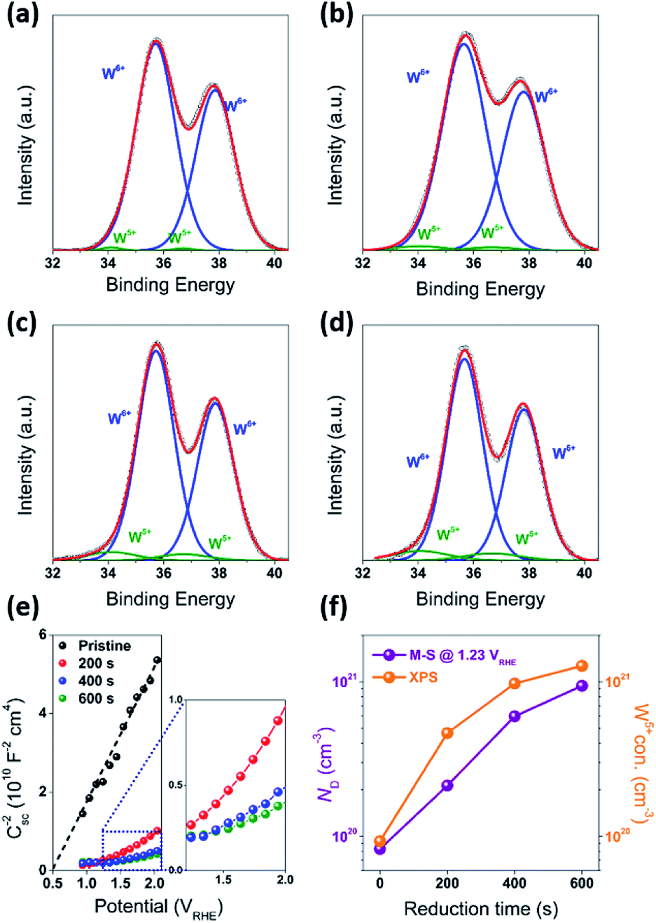
In order to understand the effect of electrodes' treatment on their structure, morphology and surface composition, a further characterization of the samples was performed by X-ray diffraction, X-ray Photoelectron Spectroscopy (XPS), Atomic Force Microscope (AFM) and Electrochemical Impedance Spectroscopy (EIS). No new X-ray diffraction peaks or significant peak shift in the existing peaks were observed for the reduced WO3 samples (Fig. S4a–c, ESI†), suggesting that the reduction treatment had a minimal effect on WO3 lattice structure. The surfaces of the pristine and reduced WO3 samples were further investigated by atomic force microscopy. The average surface roughness (Ra) for R0, R1, R2 and R3 samples was 4.5, 4.2, 5.1, and 5.4 nm, respectively. Despite the fact that the surfaces of R0, R1, and R2 samples appeared to have very similar granular structures, these structures were not present in the R3 sample reduced for the longest time (Fig. 5a–d). These results suggest that the reduction treatment has some subtle effects on WO3 morphology, although defining the trends in morphological changes might require further investigation. The effect of sample reduction on the WO3 surface composition was further studied by the XPS in conjunction with EIS measurements. Fig. 6a–d shows high-resolution W 4f spectra of the WO3 photoanodes (R0, R1, R2, and R3). It can be clearly seen that the WO3 undergo significant evolution upon the reduction treatment. The W 4f doublet at 37.7 and 35.5 eV, can be assigned to W6+ species, while 36.5 and 34.3 eV doublet can be assigned to W5+ species. A comparison between W 4f peaks for samples reduced for different times (R1–R3) indicated an increased full width at half maximum (FWHM) of the peaks as compared to that for the pristine sample (R0). Such increase can be attributed to increased contribution of W5+ species to the overall spectra with increased reduction time (Fig. 6f). More specifically, the W5+ concentration was determined based on the ratio of W6+ and W5+ peak areas. The pristine sample (R0) had W5+ atomic concentration of 0.5%, (9.2 × 1019 cm−3, W5+ concentration in volume), while the most reduced sample (R3) had an increased W5+ atomic concentration of species of 6.8%, (1.26 × 1021 cm−3 W5+ concentration in volume). It is important to note that the presence of W5+ species is indicative of oxygen vacancies formation, which act as shallow donors for n-type WO3.34 In order to understand the effect of oxygen vacancies on PEC performance, the donor densities were determined by EIS, which measured the differential capacitance Csc of the depletion region at various electrode potentials E. For a flat, uniformly doped semiconductor electrode, a linear relation between 1/C2sc and E is defined by the Mott–Schottky equation:24,35–37
 | (1) |
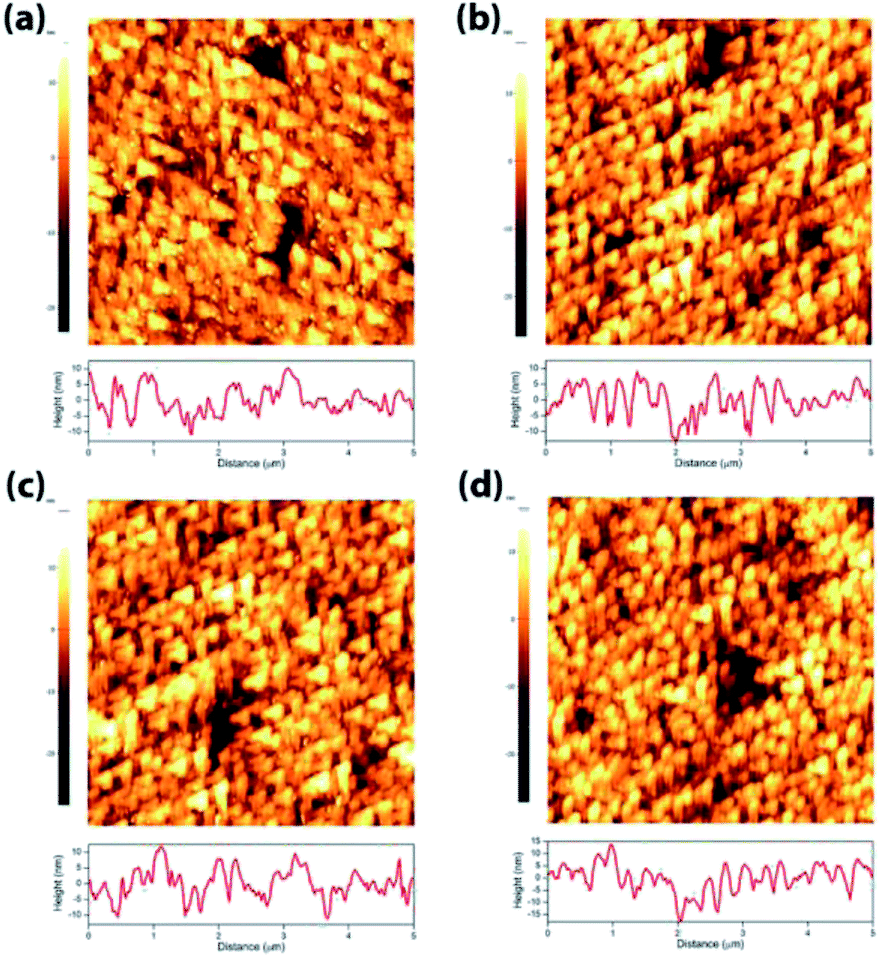 | ||
| Fig. 5 AFM for WO3 photoanodes (R0, R1, R2, and R3). | ||
 | ||
| Fig. 6 (a–d) W 4f XPS for WO3 photoanodes (R0, R1, R2, and R3). (e) Mott–Schottky plots, for pristine and WO3 photoanodes (R0, R1, R2, and R3). (f) ND and W5+ concentration as a function of reduction time. | ||
In our case, this equation was used to determine the donor density ND based on such variables as elementary charge e, the dielectric constant ε, the vacuum permittivity ε0, the flat band potential EFB and the thermal energy kBT. In our calculations the value of ε = 35 for the WO3 electrodes was based on the literature data.15 The ND value for the pristine sample (R0) was 8.3 × 1019 cm−3 with EFB = 0.5 VRHE, while ND values increased monotonically with an increased exposure time to reducing atmosphere. More specifically, the ND values for the reduced samples R1, R2, and R3 were 2.1 × 10²⁰, 6.0 × 10²⁰ and 9.4 × 1020 cm−3 respectively. It is useful to note that the donor densities determined by the EIS method were within one order of magnitude of W5+ surface densities determined by XPS, confirming a successful introduction of tunable concentration of oxygen vacancies into the WO3 surfaces by a very simple treatment.
To clarify the mechanism of the PEC enhancement by the mild reduction treatment, several factors have to be considered. Previously published modification of WO3 by various treatment methods introduced HxWO3 and/or WO3−x (W5+ and oxygen vacancies) species into WO3 photoanodes, which resulted in the enhancement of PEC water oxidation.4,28,38,39 Although the studies mentioned above focused on photoanodes having different film thickness and surface pre-treatment conditions from those used in this work, it is still instructive to analyze these published results. More specifically the literature suggests that the WO3 photoanodes containing W5+ species are highly resistive to re-oxidation and peroxo-species induced dissolution.28 while exhibiting enhanced hole transfer efficiency.4,38,39 Our calculations based on Butler–Volmer model40 also showed that the mild reduction treatment on WO3 can also enhance the absolute magnitude of the electric field (E0) at the interface between semiconductor and electrolyte (Fig. S6a, ESI†), resulting in suppressing of electron collection efficiency (Fig. S6b, ESI†).40
In addition to the above mentioned electronic effects, it is also important to consider such spatial factors as depletion width, effective minority carriers diffusion and the thickness of the higher dopant density region. These spatial factors can all be affected by the surface treatment. For example, reduction of the samples resulted in an increase in dopant concentration and decrease in a depletion width. At 1.23 VRHE, the calculated depletion width (dsc) of pristine WO3 (R0) electrode was about 7 nm, while the dsc for the reduced WO3 (R1, R2, and R3) electrodes was about 2 nm (Fig. S6c, ESI†). In the classic Gartner model, photocurrent may only be produced when photogenerated charge carriers are created within both the depletion width and effective minority carrier diffusion length (Lp). Given that the literature reported hole diffusion length for WO3 is Lp = 0.5 μm.7,40,41 while the measured sample thickness is also 0.5 μm, it is conceivable that all photogenerated holes were efficiently utilized as charged carriers that could diffuse into SCR. However, such efficient utilization of holes can't explain the difference in photocurrent and IPCE between R1, R2, and R3 electrodes, where the presence of the doped region did not improve the quantum efficiency or R2 and R3 samples across the entire spectrum. As evident from Fig. 3d, a thicker reduction region for R2 and R3 electrodes resulting from longer reduction times caused a precipitous decrease in IPCE within 300 nm to 340 nm wavelength window (Fig. 3d). To rationalize this dependence, it is important to emphasize that a mismatch between depletion and doped region widths is critical to explain such behavior. Considering that in our case the doped region is larger than the depletion region, the recombination sites for doped region of R2 and R3 electrodes most likely suppressed and quenched the photogenerated charge carriers excited by the shorter wavelength light in the 300–340 nm spectral region. However, for the mildly reduced WO3 photoanode (R1) it is conceivable that the reduction region has a better match to a depletion region. As result, the R1 electrode exhibited dramatic across 300–480 nm wavelength IPCE enhancement as compared to that for the pristine sample (Fig. 7c and d).
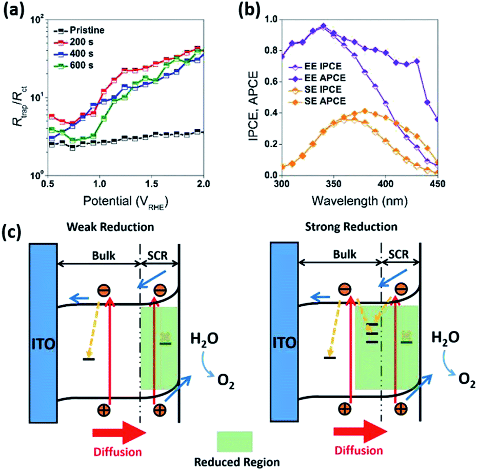 | ||
| Fig. 7 (a) Rtrap/Rct for R0, R1, R2, and R3 photoanodes under front-side (EE) illumination. (b) Back-side (semiconductor–electrolyte side, SE) and front-side (EE) IPCE and APCE measurements for the optimized WO3 photoanodes (R1), carried out at 1.23 VRHE. The characterization of the photoanodes were conducted in 0.5 M H2SO4 electrolyte. (c) Schematic band bending diagram and charge transfer processes in WO3 photoanodes after weak and strong reduction treatments. | ||
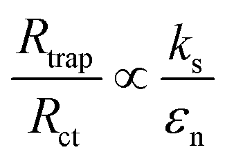
To get further understanding of the charge carriers' dynamic of at the SEI, photoelectrochemical impedance spectroscopy (PEIS) measurements were conducted at the PEC experimental conditions under illumination. These measurements allowed to model several aspects of an electrode behavior. As compared to the often used EIS equivalent model for dark condition (Fig. S5, ESI†), the equivalent circuit model utilized this our work (Fig. S7, ESI†) contains additional variables that reflect behaviors of the traps in photoanodes. These variables include a chemical capacitance (Css) representing the chemical capacitance of the traps, a trapping resistance (Rtrap) representing the trapping/detrapping resistance of electrons that go from the conduction band to the surface traps, and a charge-transfer resistance (Rct) representing the resistance of hole transfer.42,43 The dependence of these variables (Css, Rtrap, and Rct) on the applied potential measured for our samples is shown in the ESI (Fig. S7, ESI†). In order to get better insights from this dependence, it is informative to relate the hole collection efficiency to the ratio Rtrap/Rct,44 as following:
 | (2) |
3. Conclusion
In summary, WO3 thin film photoanodes were prepared by pulsed laser deposition under optimized conditions. The mild reduction treatment on WO3 photoanodes was controlled by post annealing in low oxygen partial pressure for different durations. The surface reduced of the samples was characterized by Mott–Schottky, XPS, PEC and IPCE measurements. The results work outlined the optimum conditions for the surface reduction treatment, as elevated level of defects beyond the space charge region resulted in loss of IPCE in UV region. The mildly reduced R01 sample exhibited largely improved PEC photocurrent density and IPCE across the entire 300–480 nm spectral window. This work provides a simple and well-defined roadmap for the preparation of high performance WO3 photoanodes by mild surface modulation. This approach might be also promising for other semiconductors with small dielectric constants, which can potentially include α-Fe2O3 and TiO2 based electrodes.4. Experimental section
4.1 Thin film fabrication
WO3 thin films were grown by pulsed laser deposition (PLD/MBE-2300, PVD Products) on indium tin oxide (ITO) glass substrates (Thin Film Devices, 20 Ω sq−1). More specifically, a ceramic WO3 target was prepared by cold-pressing WO3 powder into a cylindrical pellet, which was finally sintered at 1100 °C for 12 hours. The WO3 target was ablated by KrF excimer laser pulses (λ = 248 nm) at a fixed repetition rate of 5 Hz, with a laser fluence of 1.5 J per cm2 per pulse. The substrate was placed 60 mm away from the target and heated to 500 °C by a non-contact radiative heating system under a controlled oxygen pressure (10–300 mTorr). The deposition rate for WO3 was about 0.15 Å per pulse. After the deposition, the substrate was cooled down at a constant rate of 10 °C min−1 to a room temperature. The surface of the samples was reduced by post annealing at 500 °C under 95 mTorr oxygen pressure for 200–600 seconds. Samples reduced for 0, 200, 400, and 600 seconds were labelled as R0, R1, R2, and R3 respectively.4.2 Characterization
The X-ray diffraction patterns were recorded by an Ultima III diffractometer with parallel beam optics using Cu-Kα radiation (λ = 1.54184 Å). Optical characterization was performed in a Lambda 950 UV-vis-NIR spectrometer (PerkinElmer) equipped with a 150 mm integrating sphere. Scanning electron microscopy images were obtained using a HITACHI 4800 SEM at an accelerating voltage of 10 kV. The cross sections of the samples were prepared by focused ion beam in situ liftout using an FEI Helios dual beam SEM-FIB system. The X-ray photoelectron spectroscopy was performed in an ultra-high vacuum (UHV) chamber equipped with a hemispherical electron energy analyzer (Thermo Fisher Scientific, Alpha 110) and an Al/Mg twin anode X-ray source (Thermo Fisher Scientific, T352/NT).4.3 Photoelectrochemical measurements
PEC measurements were performed in a custom-built, three-electrode cell with a quartz viewing window. The cell included a working photoanode, an Hg/Hg2SO4/saturated K2SO4 reference electrode (0.640 VNHE, WPI Inc.), and a platinum wire counter electrode. A 1.0 cm2 area of the working electrode was exposed to the electrolyte and illuminated from the front-side through the quartz window or the back-side through the ITO glass. The electrolyte was an aqueous solution of 0.5 M H2SO4 (pH ∼0.3). The linear sweep voltammetry (LSV) was performed with a sweep rate of 50 mV s−1 under dark or under simulated AM 1.5G illumination, using a Newport-Oriel 150 W Xenon arc lamp fitted with an AM 1.5G filter. The incident illumination power of 100 mW cm−2 was measured by a calibrated Si detector (Newport). The potentials referenced to the Hg/Hg2SO4 reference electrode were converted to potentials referenced to the reversible hydrogen electrode (RHE) using the Nernst equation,| ERHE = EHg/Hg2SO4 + 0.0591V × pH + 0.682V | (3) |
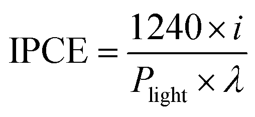
The monochromatic illumination for the IPCE measurements utilized a 300 W xenon arc lamp (Newport) coupled to a 1/8 m grating monochromator (Newport CS130), which was equipped with order sorting filters. The incident power was measured with an optical power meter (Newport 1918 C) and a UV-enhanced Si photodiode sensor. The IPCE is calculated based on the following equation,
 | (4) |
Conflicts of interest
There are no conflicts to declare.Acknowledgements
We acknowledge funding support from the National Science Foundation (#1254600). This research used resources of the Center for Functional Nanomaterials, which is a U. S. DOE Office of Science Facility, at Brookhaven National Laboratory under Contract No. DE-SC0012704.Notes and references
- G. Hodes, D. Cahen and J. Manassen, Nature, 1976, 260, 312–313 CrossRef CAS
.
- M. Carmo, D. L. Fritz, J. Merge and D. Stolten, Int. J. Hydrogen Energy, 2013, 38, 4901–4934 CrossRef CAS
- V. S. Vidyarthi, M. Hofmann, A. Sayan, K. Sliozberg, D. Konig, R. Beranek, W. Schuhmann and A. Ludwig, Int. J. Hydrogen Energy, 2011, 36, 4724–4731 CrossRef CAS
- M. Ma, K. Zhang, P. Li, M. S. Jung, M. J. Jeong and J. H. Park, Angew. Chem., Int. Ed. Engl., 2016, 55, 11819–11823 CrossRef CAS PubMed
- M. Balandeh, A. Mezzetti, A. Tacca, S. Leonardi, G. Marra, G. Divitini, C. Ducati, L. Meda and F. Di Fonzo, J. Mater. Chem. A, 2015, 3, 6110–6117 RSC
- S. Shin, H. S. Han, J. S. Kim, I. J. Park, M. H. Lee, K. S. Hong and I. S. Cho, J. Mater. Chem. A, 2015, 3, 12920–12926 RSC
- H. Wang, T. Lindgren, J. He, A. Hagfeldt and S.-E. Lindquist, J. Phys. Chem. B, 2000, 104, 5686–5696 CrossRef CAS
- T. Li, J. He, B. Pena and C. P. Berlinguette, ACS Appl. Mater. Interfaces, 2016, 8, 25010–25013 CrossRef CAS PubMed
- Y. Liu, J. Li, W. Li, H. He, Y. Yang, Y. Li and Q. Chen, Electrochim. Acta, 2016, 210, 251–260 CrossRef CAS
- Y. Liu, J. Li, W. Z. Li, Y. H. Yang, Y. M. Li and Q. Y. Chen, J. Phys. Chem. C, 2015, 119, 14834–14842 CrossRef CAS
- Y. Liu, J. Li, H. Tang, W. Z. Li, Y. H. Yang, Y. M. Li and Q. Y. Chen, Electrochem. Commun., 2016, 68, 81–85 CrossRef CAS
- Y. Liu, Y. Yang, Q. Liu, Y. Li, J. Lin, W. Li and J. Li, J. Colloid Interface Sci., 2018, 512, 86–95 CrossRef CAS PubMed
- Y. Liu, Y. H. Yang, Q. Liu, H. Z. He, W. H. Liu, D. D. Meng, Y. M. Li, W. Z. Li and J. Li, Int. J. Hydrogen Energy, 2018, 43, 208–218 CrossRef CAS
- J. Yan, T. Wang, G. Wu, W. Dai, N. Guan, L. Li and J. Gong, Adv. Mater., 2015, 27, 1580–1586 CrossRef CAS PubMed
- C. A. Bignozzi, S. Caramori, V. Cristino, R. Argazzi, L. Meda and A. Tacca, Chem. Soc. Rev., 2013, 42, 2228–2246 RSC
- A. Tacca, L. Meda, G. Marra, A. Savoini, S. Caramori, V. Cristino, C. A. Bignozzi, V. Gonzalez Pedro, P. P. Boix, S. Gimenez and J. Bisquert, ChemPhysChem, 2012, 13, 3025–3034 CrossRef CAS PubMed
- R. H. Coridan, K. A. Arpin, B. S. Brunschwig, P. V. Braun and N. S. Lewis, Nano Lett., 2014, 14, 2310–2317 CrossRef CAS PubMed
- J. M. Spurgeon, J. M. Velazquez and M. T. McDowell, Phys. Chem. Chem. Phys., 2014, 16, 3623–3631 RSC
- C. C. McCrory, S. Jung, I. M. Ferrer, S. M. Chatman, J. C. Peters and T. F. Jaramillo, J. Am. Chem. Soc., 2015, 137, 4347–4357 CrossRef CAS PubMed
- J. W. Huang, Y. Zhang and Y. Ding, ACS Catal., 2017, 7, 1841–1845 CrossRef CAS
- J. Zhang, Z. Liu and Z. Liu, ACS Appl. Mater. Interfaces, 2016, 8, 9684–9691 CrossRef CAS PubMed
- C. Liu, Y. Yang, W. Li, J. Li, Y. Li and Q. Chen, Sci. Rep., 2016, 6, 23451 CrossRef CAS PubMed
- C. Cheng, J. Shi, Y. Hu and L. Guo, Nanotechnology, 2017, 28, 164002 CrossRef PubMed
- J. Cen, Q. Wu, M. Liu and A. Orlov, Green Energy & Environment, 2017, 2, 100–111 Search PubMed
- H. Hamdi, E. K. H. Salje, P. Ghosez and E. Bousquet, Phys. Rev. B, 2016, 94, 245124 CrossRef
- J. M. Berak and M. J. Sienko, J. Solid State Chem., 1970, 2, 109–133 CrossRef CAS
- M. Sarnowska, K. Bienkowski, P. J. Barczuk, R. Solarska and J. Augustynski, Adv. Energy Mater., 2016, 6, 1600526 CrossRef
- G. M. Wang, Y. C. Ling, H. Y. Wang, X. Y. Yang, C. C. Wang, J. Z. Zhang and Y. Li, Energy Environ. Sci., 2012, 5, 6180–6187 RSC
- O. Zandi, A. R. Schon, H. Hajibabaei and T. W. Hamann, Chem. Mater., 2016, 28, 765–771 CrossRef CAS
- M. F. Daniel, B. Desbat, J. C. Lassegues, B. Gerand and M. Figlarz, J. Solid State Chem., 1987, 67, 235–247 CrossRef CAS
- C. Santato, M. Odziemkowski, M. Ulmann and J. Augustynski, J. Am. Chem. Soc., 2001, 123, 10639–10649 CrossRef CAS PubMed
- C. V. Ramana, S. Utsunomiya, R. C. Ewing, C. M. Julien and U. Becker, J. Phys. Chem. B, 2006, 110, 10430–10435 CrossRef CAS PubMed
- I. M. Szilagyi, B. Forizs, O. Rosseler, A. Szegedi, P. Nemeth, P. Kiraly, G. Tarkanyi, B. Vajna, K. Varga-Josepovits, K. Laszlo, A. L. Toth, P. Baranyai and M. Leskela, J. Catal., 2012, 294, 119–127 CrossRef CAS
- S. K. Deb, Phys. Rev. B, 1977, 16, 1020–1024 CrossRef CAS
- M. Z. Liu, J. L. Lyons, D. H. Yan and M. S. Hybertsen, Adv. Funct. Mater., 2016, 26, 219–225 CrossRef CAS
- A. J. Bard and L. R. Faulkner, Electrochemical Methods: Fundamentals and Applications, Wiley, NJ, US, 2 edn, 2000 Search PubMed
- J. Cen, Q. Wu, D. Yan, J. Tao, K. Kisslinger, M. Liu and A. Orlov, Phys. Chem. Chem. Phys., 2017, 19, 2760–2767 RSC
- H. D. Zheng, J. Z. Ou, M. S. Strano, R. B. Kaner, A. Mitchell and K. Kalantar-Zadeh, Adv. Funct. Mater., 2011, 21, 2175–2196 CrossRef CAS
- W. Li, P. Da, Y. Zhang, Y. Wang, X. Lin, X. Gong and G. Zheng, ACS Nano, 2014, 8, 11770–11777 CrossRef CAS PubMed
- M. A. Butler, J. Appl. Phys., 1977, 48, 1914–1920 CrossRef CAS
- R. A. Pala, A. J. Leenheer, M. Lichterman, H. A. Atwater and N. S. Lewis, Energy Environ. Sci., 2014, 7, 3424–3430 RSC
- Q. Shi, S. Murcia-Lopez, P. Y. Tang, C. Flox, J. R. Morante, Z. Y. Bian, H. Wang and T. Andreu, ACS Catal., 2018, 8, 3331–3342 CrossRef CAS
- F. Le Formal, N. Tétreault, M. Cornuz, T. Moehl, M. Grätzel and K. Sivula, Chem. Sci., 2011, 2, 737–743 RSC
- G. M. Carroll and D. R. Gamelin, J. Mater. Chem. A, 2016, 4, 2986–2994 RSC
- W. R. Zhang, D. H. Yan, J. Li, Q. Y. Wu, J. J. Cen, L. H. Zhang, A. Orlov, H. L. Xin, J. Tao and M. Z. Liu, Chem. Mater., 2018, 30, 1677–1685 CrossRef CAS
- R. Zhang, F. Ning, S. Xu, L. Zhou, M. Shao and M. Wei, Electrochim. Acta, 2018, 274, 217–223 CrossRef CAS
Footnote |
| † Electronic supplementary information (ESI) available. See DOI: 10.1039/c8ra08875f |
| This journal is © The Royal Society of Chemistry 2019 |