
 Open Access Article
 This Open Access Article is licensed under a Creative Commons Attribution-Non Commercial 3.0 Unported Licence
Interface-governed nanometric machining behaviour of Cu/Ag bilayers using molecular dynamics simulation
Qihong Fanga,
Yuanyuan Tian a,
Jia Li*a,
Qiong Wanga and
Hong Wub
a,
Jia Li*a,
Qiong Wanga and
Hong Wub
aState Key Laboratory of Advanced Design and Manufacturing for Vehicle Body, Hunan University, Changsha, 410082, PR China. E-mail: lijia123@hnu.edu.cn
bState Key Laboratory of Powder Metallurgy, Central South University, Changsha, 410083, PR China
First published on 11th January 2019
Abstract
The nanometric machining of Cu/Ag bilayers and pure Cu film is performed using molecular dynamics (MD) simulations. The mechanical and tribological properties of Cu/Ag bilayers are investigated by comparing with those of pure Cu film. The effects of machining parameters (indenter radius, tool speed and machining depth) on the subsurface damage and material removal are studied by analyzing the dislocation movement, chipping volume, machining force and average temperature of the workpiece. The results show that the hardness of Cu/Ag bilayers is smaller than that of pure Cu film, due to the dislocation nucleation and emission from the Cu/Ag interface. Meanwhile, the friction coefficient of Cu/Ag bilayers is larger than that of pure Cu film. Furthermore, the metal bonding energy at the Cu/Ag interface is weaker than that in pure Cu film, which causes the low hardness in the Cu/Ag bilayers. The Young's moduli in the Cu/Ag bilayers and pure Cu film are calculated by the Hertz contact mechanism and are close to the experimental result. During nanometric machining of Cu/Ag bilayers, the larger indenter radius or higher tool speed would cause a larger indentation force. The chipping volume, machining force and average temperature would increase with the increment of indenter radius, tool speed and machining depth. The subsurface damage can be reduced by selecting the smaller indenter radius, lower tool speed, and smaller machining depth, where fewer lattice defects are produced. In addition, the selection of lower tool speed also plays a crucial role in improving the smoothness of the ground surface.
1. Introduction
Nanoscale bilayer materials possess high strength,1–3 good stability and ductility,4,5 and strong fracture toughness,6 which demonstrates their great potential application as hard coatings, in aerospace equipment, X-ray optics and nano-electro-mechanical systems (NEMS).7–11 However, nanoscale bilayer materials are routinely underutilized because of high machining cost and lower machining efficiency. Thus the deformation behaviors as property indicators are fully analyzed to further understand the machining of these materials in the nanoscale level,12–15 thereby improving the machining properties and efficiency. Experimental observation often has the features of uncertain measurements, high costs and long time durations.14,15 Therefore, MD simulation is applied to track the deformation dynamics, identify the defect structure and reveal the deformation mechanism in nanoscale bilayer or polycrystal materials.16,17 A number of MD simulation studies have provided valuable insights into the ultra-precision machining of bilayers. For example, Cao et al. investigated the mechanical and tribological properties of Ni/Al bilayers.18 Shao et al. explored the dislocation–interface interaction during nanoindentation of Cu/Ni bilayers.19 Fang et al. revealed the nanoindentation mechanisms and mechanical responses of Al/Ni bilayered films.20 Cheng et al. studied the effect of misfit dislocations on the tribological behavior of Cu/Ni bilayers.21 Although the above studies are important for us to promote understanding of the deformation behaviors and properties in metal bilayers, the Cu/Ag bilayer materials are regrettably little-studied at the nanoscale. Cu/Ag bilayer materials are commonly used in engineering fields because of their strong anti-oxidation properties, good electrical and thermal conductivity, and high strength.22–24 According to the actual physical system mentioned in the experiment of Cu/Ag multilayers,22 the model of Cu/Ag bilayers is built in the current simulation to investigate the interface-governed nanometric machining behaviour for Cu/Ag bilayers. In addition, as the Cu and Ag metals are current-carriers, the electrical conductivity of Cu/Ag alloy is weaker than that of the Cu/Ag bilayers. Hence, the current Cu/Ag model is set as a bilayer system. The nanoindentation of Cu/Ag bilayers had been conducted by MD simulations to clarify the plastic deformation mechanism controlled by Cu/Ag interface in our previous work,25 but the effect of Cu/Ag interface on the mechanical and tribological properties, including hardness and friction coefficient, as well as the subsurface damage and material removal during the nanometric machining of Cu/Ag bilayers with the various machining parameters have not been studied detailedly so far.Therefore, in this paper, MD simulations are conducted to investigate the mechanical and tribological properties of Cu/Ag bilayers during nanometric machining. The indentation force, Young's modulus, indentation hardness, and friction coefficient of Cu/Ag bilayers are investigated by comparing with those of pure Cu film. In addition, the effects of machining parameters on the subsurface damage and material removal are discussed via analyzing the dislocation movement, chipping volume, machining force and average temperature of workpiece. The MD simulations are helpful to understand the effect of interface on the mechanical and tribological properties and the machining properties of bilayer material from atomic level, which is beneficial for developing ultra-precision machining of bilayer materials.
2. Simulation method
Fig. 1 shows the MD simulation model for nanometric machining of Cu/Ag bilayers. The model comprises a rigid diamond tool and a workpiece of Cu/Ag bilayers. In order to reveal the interface effect on the mechanical and tribological properties of Cu/Ag bilayers, the pure Cu film with the same dimension is introduced as a workpiece for nanometric machining. Table 1 gives simulation parameters of the Cu/Ag bilayers, pure Cu film and tool. The diamond tool has a spherical shape with selected radii of 3.0 nm, 4.0 nm and 5.0 nm. The tool is seen as a rigid body in the simulations because the stiffness of diamond is far larger than that of Cu or Ag metals. The Cu/Ag bilayers consist of Ag substrate and Cu thin film. The Ag substrate with three orientations of x-[1 0 0], y-[0 1 0] and z-[0 0 1] has a size of 14 nm × 22 nm × 6 nm. The Cu thin film with a layer thickness of 3 nm is bonded to the top of Ag substrate. The three orientations of Cu thin film are in x-[1 0 0], y-[0 1 0] and z-[0 0 1], respectively. The size of pure Cu film is 14 nm × 22 nm × 9 nm, and x-[1 0 0], y-[0 1 0] and z-[0 0 1] are three orientations of the pure Cu film. The nanometric machining is conducted along [0 1 0] direction on (0 0 1) surface of workpiece. Both x and y directions are set as the periodic boundary conditions to avoid the effect of simulation length-scale. The positive direction of z-axis is defined to be free because the (001) surface of workpiece is machined. There are three types of atoms in the workpiece: Newtonian atoms, thermostat atoms and boundary atoms. The boundary atoms are fixed to prevent the rigid body motion of workpiece. The slip behavior between Cu film and Ag substrate is ignored as the slip speed is far slower than the speed of dislocation motion, and the machining distance is shorter during the nanometric machining. The thermostat atoms are set to carry out the dissipation of heat generated the nanometric machining. The motion of Newtonian and thermostat atoms follows classical Newton's second law whose motion equations are integrated by the velocity-Verlet numerical integration algorithm. The initial temperature of workpiece is set as 293 K. The initial velocity of atoms is assigned on account of Maxwell–Boltzman distribution. During the MD simulation process, the average temperature of workpiece is calculated from the equation:
 | (1) |
 | ||
| Fig. 1 MD simulation model for the nanometric machining of Cu/Ag bilayers. | ||
| Models | Workpiece: Cu/Ag bilayers and pure Cu film | Tool: diamond |
| Dimensions | 14 nm × 22 nm × 9 nm | Radii 3, 4 and 5 nm |
| Time step | 1 fs | |
| Initial temperature | 293 K | |
| Tool speed | 20, 100 and 200 m s−1 | |
| Machining depth | 1, 1.5 and 2. 5 nm | |
| Machining distance | 0–10 nm | |
| Machining direction | [0 1 0] on (001) surface |
The MD simulation of nanometric machining includes three stages: the relaxation stage, the nanoindentation stage and the nanoscratching stage. Whether the workpiece reaches the equilibrium state in the relaxation stage would extremely affect the subsequent nanoindentation and nanoscratching stages, because it directly affects the stability of the defect structure during the plastic deformation of workpiece. When the average temperature of workpiece slightly fluctuates around a stable value, the workpiece reaches the equilibrium state in the relaxation stage. In addition, the change of temperature should be considered in the nanoindentation and nanoscratching stage due to the increased effect of heat on the workpiece deformation at the nanometer scale. So, we adopt the NVE ensemble in Newtonian atom layers of the workpiece,10 to relax the workpiece to its equilibrium state with using the velocity scaling method in the relaxation stage and constrain the workpiece in the following nanoindentation and nanoscratching stages. It takes 50 ps for the relaxation stage. After that, the equilibrium configurations are obtained for the Cu/Ag bilayers and pure Cu film. The tool presses into workpiece uniformly along the negative z-axis until the desired indentation depth is reached, and then the nanoscratching is performed by moving tool along the positive y-direction, as shown in Fig. 1. Specially, the considerable heat is produced from machined zone during nanoindentation and nanoscratching processes, thus the heat dissipation is carried out by maintaining the temperature of thermostat layer at the constant temperature of 293 K with the usage of the velocity rescaling method. The velocities of thermostat atoms are rescaled at every ten time steps when the temperature departs more than 10 K of 293 K. This algorithm makes the heat from the machined region on the surface is transfered to the bulk of workpiece, which is similar to experiment. This method above mentioned has widely been applied to study the nano-machining, nano-scratching, nano-grinding, nano-cutting and nanoindentation.10,19,20,25,26 Due to that the different machining speeds are applied to the nanometric machining, the time length of simulations ranges from 110 to 500 ps. All simulations are performed by the classic MD code LAMMPS (the “15 May 2015” version) with a time step of 1 fs.27 The MD data is visualized and the MD snapshot is exhibited by the software OVITO (the “2.8.0” version).28 The common neighbor analysis (CNA) is utilized to identify the atom features before and after nanometric machining.29 Atoms are colored in accordance with the calculated CNA values: red atoms are intrinsic stacking fault (ISF) atoms, green atoms are FCC atoms, gray atoms are other atoms including surface atoms and dislocation cores, and BCC atoms are indicated in blue.
In addition, the selection of interaction potential function play a significant role in ensuring the accuracy of the simulation results. There are five kinds of atomic interactions in the MD simulations: (1) the interaction between the diamond tool atoms (C–C), which is ignored since the diamond tool is seen as a rigid body in the present simulations. (2) The interaction between the diamond tool and workpiece atoms (C–Cu), which is described by the Morse potential derived from the equation:30–35
 | (2) |
3. Mechanical and tribological properties
Fig. 2a–d is the x–y sectional views of interface mismatch dislocations in Cu/Ag interface on the (001) plane for the different Cu film thicknesses. As a result, a semi-coherent interface is formed in Cu/Ag bilayers.25 It is observed that the mismatch dislocations are arranged periodically as a network structure along the interface.3,25 The interface structure is obviously stable when the Cu film thickness is larger than 3 nm. In addition, the interface mismatch dislocations on different crystal planes of (110) and (111) with the Cu film thickness of 6 nm are shown in Fig. 2e and f, indicating the crystal plane dominated the interface mismatch dislocation. In the current study, the Cu film thickness of 3 nm and (001) plane are selected to investigate the interface-governed nanometric machining behaviour of Cu/Ag bilayers.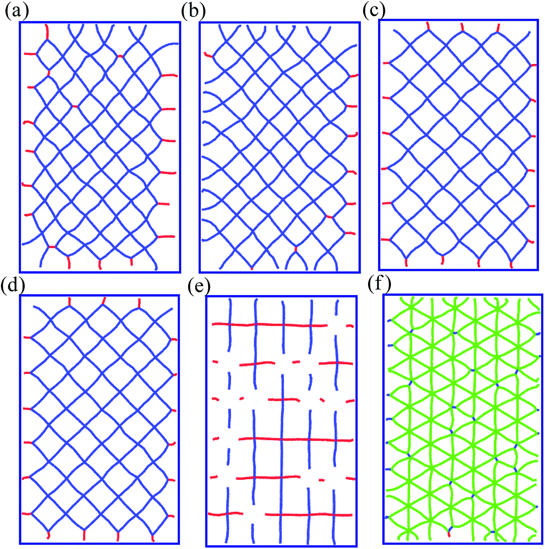 | ||
| Fig. 2 The x–y sectional views of interface mismatch dislocations at different Cu film thicknesses: 1 nm (a), 2 nm (b), and 3 nm (c), and 10 nm (d) on the (001) plane. Interface mismatch dislocations at the Cu film thickness of 6 nm and different crystal planes: the (110) plane (e), and the (111) plane (f). | ||
The Young's modulus of material is a key indicator, to assess the mechanical properties. Based on the Hertz contact mechanism,18 Young's modulus of the substrate (Cu/Ag bilayers and pure Cu film) is given as followed:
 | (3) |
 | (4) |
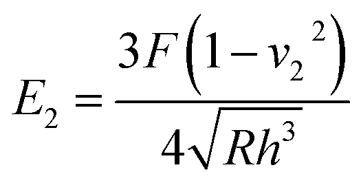
According to eqn (4) and Fig. 3a, Young's modulus in Cu/Ag bilayers and pure Cu film is calculated as 105 GPa and 123 Gpa, which is consistent with the previous experiment results of 115 GPa and 129 GPa.39–41
 | ||
| Fig. 3 Relationship of indentation force versus indentation depth (a). The x–z sectional views of the Cu/Ag interface at the indentation depths: 1.45 nm (b), and 1.5 nm (c). The atomic electron density maps in pure Cu film (d) and Cu/Ag interface (e). (I) The dislocation propagation through the interface from the Cu film into Ag substrate. (II and III) The dislocation nucleation and emission from the interface into the Cu film. (IV) The dislocation nucleation and emission from the interface into the Ag substrate. | ||
The hardness measurement is important for the evaluation of mechanical properties of materials. According to the previous work,42 the hardness H, sometimes referred to as the contact pressure, is calculated as followed:
 | (5) |
| A = π(2r − hmax)hmax | (6) |
Hence, the hardness can be obtained by the equation:
 | (7) |
Based on eqn (7), the hardness of pure Cu film is calculated as 14.6 GPa, which is closed to the simulation value of 14 GPa46 and the experiment value of 12.4 GPa.47 The hardness of Cu/Ag bilayers is calculated as 10.3 GPa, and smaller than that of pure Cu film.
Fig. 3a shows the curves of indentation force versus the indentation depth. Here, the indentation force is defined as the force acting on the indenter along z-direction, which is measured by summing the forces of all the indenter atoms along z direction.37 The indentation forces firstly increase linearly, indicating the occurrence of the elastic deformation. After the elastic deformation, the indentation forces fluctuate owing to the dislocation movement. As a result, the plastic deformation occurs in Cu/Ag bilayers and pure Cu film.
Low Young's modulus and hardness above mentioned are attributed to the interface-weakening effect. In order to reveal the interface-weakening effect in Cu/Ag bilayers, the x–z sectional views of Cu/Ag interface are shown in Fig. 3b and c. As the indenter penetrates into Cu/Ag bilayers during nanoindentation, a few dislocations propagate through the interface (I in Fig. 3b), and more dislocations are piled up at the interface. As a result, the mismatch dislocation network deforms, which inevitably leads to the severe local mismatch strain and stress concentrated in the core region of the mismatch dislocations, and lots of strain energy stored in the interface. Consequently, the new stacking faults in different slipping systems are activated from the Cu/Ag interface. The dislocations nucleate from the interface and emit into Cu film and Ag substrate to release the strain energy (II, III and IV in Fig. 3b and c), which makes the plastic deformation more easily in the Cu/Ag bilayers. Thus, the hardness of Cu/Ag bilayers is smaller than that of pure Cu film. In addition, the smaller hardness of Cu/Ag bilayers can also be understood from the electronic level. The electron density maps of atoms in the pure Cu film and Cu/Ag interface are plotted in Fig. 3d and e. The contours run from 0 to 1 electrons per Å3. It is seen from Fig. 3e that the electron density between Cu and Ag atoms is significantly smaller than that between Cu and Cu atoms in the Cu/Ag interface. Thus the bonding energy of Cu–Ag atoms is obviously weaker than that of Cu–Cu atoms in the Cu/Ag interface. Furthermore, the existence of Cu/Ag interface reduces the bonding energy of Cu–Cu atoms near the Cu/Ag interface (Fig. 3d and e). Hence the bond strength decreases due to the localization of the electron density, which is in good agreement with the previous work.48 The bond strength strongly influences, or even determines the hardness of solid.49 Thus the smaller hardness for Cu/Ag bilayers than pure Cu film can also be explained by the electron density and bond strength.
In order to reveal the effect of interface on the deformation of Cu/Ag bilayers during the nanometric machining, the changed interface energy is presented in Fig. 4a. With the tool advancing, the interface energy firstly increases and then tends to be stable, attributed to the effect of heat produced by machining.26 In addition, the interface energy fluctuates frequently during the nanometric machining, indicating the dislocation nucleation in the Cu/Ag interface at those points. Hence, the interface energy of Cu/Ag interface plays a significant role in the plastic deformation of Cu/Ag bilayers at the machining stage as well as the nanoindentation stage.25
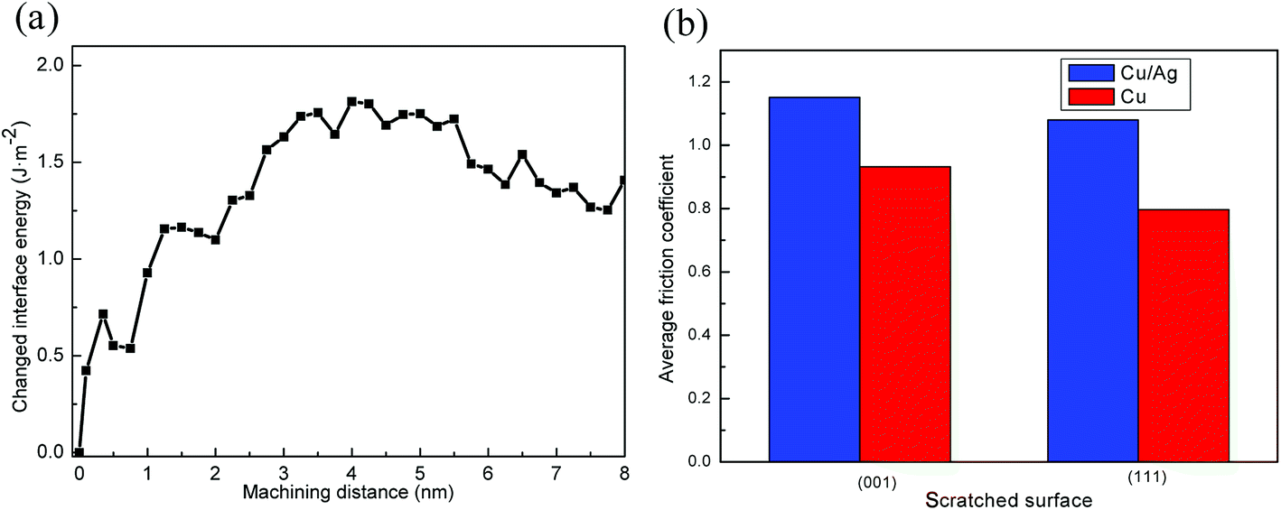 | ||
| Fig. 4 The changed interface energy during nanometric machining of Cu/Ag bilayers (a). Average friction coefficients on the machined surface of (001) and (111) in Cu/Ag bilayers and pure Cu film (b). | ||
The tribological property of Cu/Ag bilayers can be expressed by the friction coefficient during nanometric machining process. In the current study, the friction coefficient is defined as the ratio of tangential force to normal force. According to the previous work,50 the surface energy plays a key role in the friction coefficient. Fig. 4b shows the average friction coefficient on the surfaces of (001) and (111) in pure Cu film during the stable machining stage. The friction coefficient on (001) surface is larger than that on (111) surface, attributed to that the surface energy of 2.166 J m−2 on surface (001) is larger than that of 1.952 J m−2 on surface (111) in pure Cu.51 The increase in surface energy could lead to an increase in the adhesion force.50 Hence, the friction coefficient decreases if Cu (111) surface instead of Cu (001) surface.50 In addition, for Cu/Ag bilayers, the average friction coefficient on (001) surface is also higher compared to the (111) surface. Moreover, the Cu/Ag bilayers have high friction coefficient, owing to the interface softening effect to increase the adhesion force.
4. Effect of machining parameters
The machining parameters, including tool radius, machining speed, machining direction and machining depth, would influence the subsurface damage and material removal during nanometric machining of Cu/Ag bilayers. Here, the average machining temperature, machining force and defect are carefully analyzed, to gain a good ground surface and low subsurface damage. In order to clearly understand the current study, the schematic illustration for the nanometric machining is shown in Fig. 5.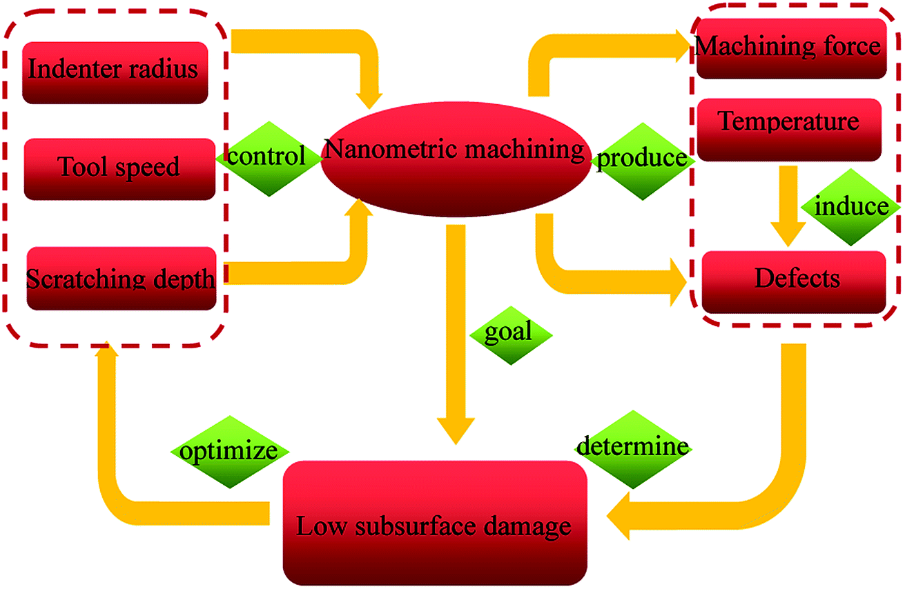 | ||
| Fig. 5 The schematic illustration for the nanometric machining of Cu/Ag bilayers. | ||
4.1. Effect of tool radius
Fig. 6a shows the variation curves of the average temperature during nanoindentation of Cu/Ag bilayers with different tool radii. The temperature rises as the indenter penetrates, and a larger indenter radius results in a higher temperature. This is because more severe extrusion occurs between atoms due to larger indentation depth or larger indenter radius. The extrusion would lead to the deformation of crystal lattices, and the strain energy is stored in deformation zone. Later the energy is released and transformed to heat when reaches the critical value. Thus, more thermal energy is produced by larger indenter radius. Fig. 6b reveals that the larger indentation force is required under larger indenter radius. Namely, a larger tool–workpiece interaction zone is formed by a larger indenter radius. Therefore, more chippings are produced and larger indentation force is necessary to maintain the tool penetration with the certain speed.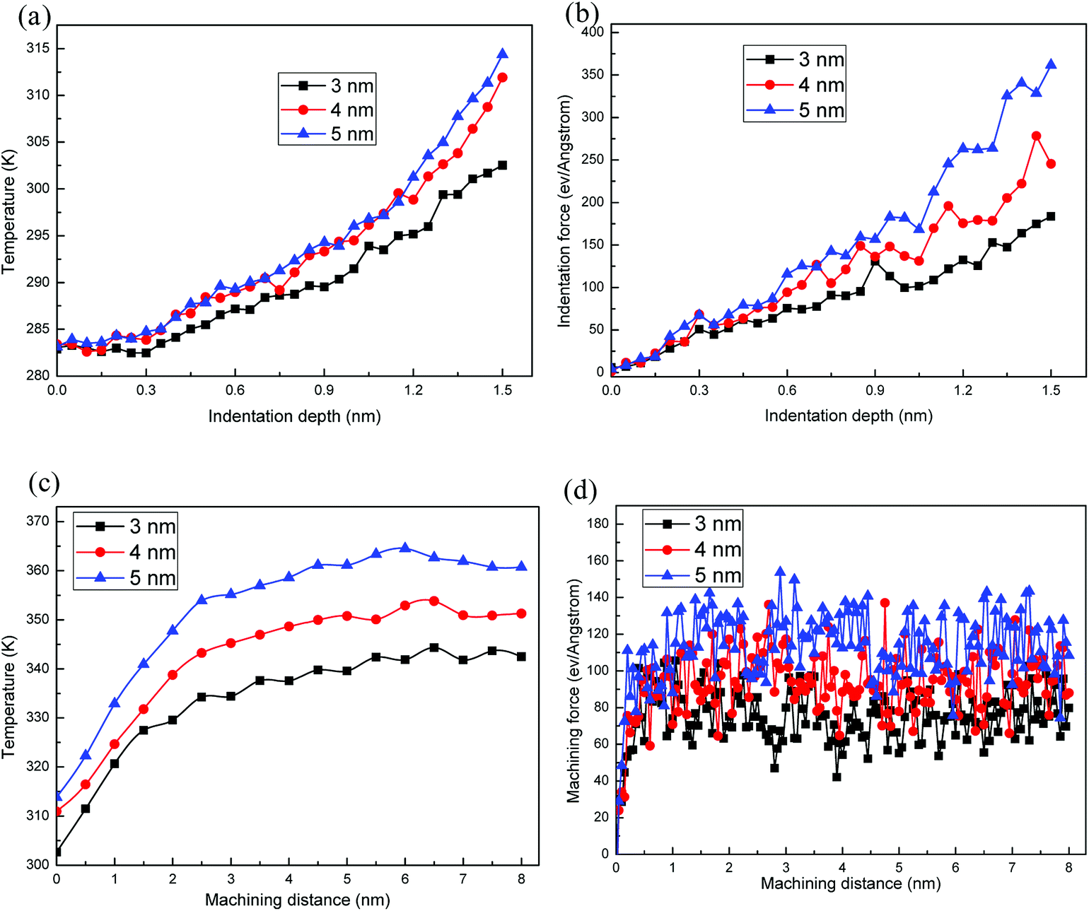 | ||
| Fig. 6 The average temperature (a) and indentation force (b) versus indentation depth. The average temperature (c) and machining force (d) versus machining distance during the nanometric machining of Cu/Ag bilayers with different tool radii of 3, 4 and 5 nm. | ||
The variation curves of the average temperature during nanometric machining with different tool radii of 3 nm, 4 nm and 5 nm are shown in Fig. 6c. Due to the effect of indenter radius on the temperature during nanoindentation process (Fig. 6a), there is a higher initial temperature in case of a larger indenter radius for the nanoscratching. The Cu/Ag bilayers have a good thermal conductivity, thus the heat from the machined region can be transferred to thermostat atoms during nanoscratching process. However, Fig. 6c shows that the average temperature keeps rising and then steady as the tool advances. This is because the temperature little diffuses from the machined region to the thermostat atoms at beginning of the scratching stage, and then the heat dissipation rate sharply increases with the increment of the machining distance, until the balance between heat dissipation rate and the heat production rate.26 Thereby the average temperature is finally stabilized at a constant. In addition, the temperature increases with the increment of indenter radius. The smaller indenter radius produces less thermal energy and makes temperature of workpiece balanced more quickly. With the increment of machining distance, the machining force first increases rapidly because of the increased atom number around the indenter, and then fluctuates nearby the corresponding constant values, as shown in Fig. 6d. The fluctuation is due to the occurrence of dislocation events during nanometric machining process. The glide of dislocations successively emitted from the tool–workpiece interaction zone leads to the increment of machining force. The dislocations passed through Cu/Ag interface, and the dislocations nucleated and emitted from the interface release the strain energy and cause the decrease of machining force. In addition, as the larger indenter radius induces more lattice defects in the machining zone, thus Cu/Ag bilayers are strengthened and larger machining force is required to maintain indenter advancing at a constant speed.
In addition, the friction coefficients of Cu/Ag bilayers and pure Cu film fluctuate with the increasing machining distance, attributed to the normal vibration of crystal lattice and the work-hardening during the nanometric machining process.50
The y–z plane cross-section snapshot of Cu/Ag bilayers for three different tool radii is shown in Fig. 7a–c, and the top view of surface morphology is presented in Fig. 7d–f. As the tool advances, the primary shear stress would be larger than the critical shear stress required for dislocation nucleation and slipping, which releases the strain energy in Cu/Ag bilayers. Fig. 7a–c indicates that the atomic lattice distortion becomes severer under the larger indenter radius. In addition, the thermal activation induced larger indenter radius also promotes the formation of defects. Thus the number of ISF atoms increases and more dislocations nucleate in case of larger indenter radius. Fig. 7d–f shows the surface morphology of Cu/Ag bilayers with different indenter radii. There is less volume of the chipping around the ground surface at smaller indenter radius. As the machining distance increases, more atoms are accumulated. Later the atoms emerge on the surface and grow into chipping. The chipping formation is a atomic extrusion process,52–54 during which dislocations nucleate, glide on the {111} slip planes and lastly terminate at the workpiece surface.9,55 Base above discussions, the smaller indenter radius should be selected to reduce the subsurface damage during the nanometric machining process of Cu/Ag bilayers.
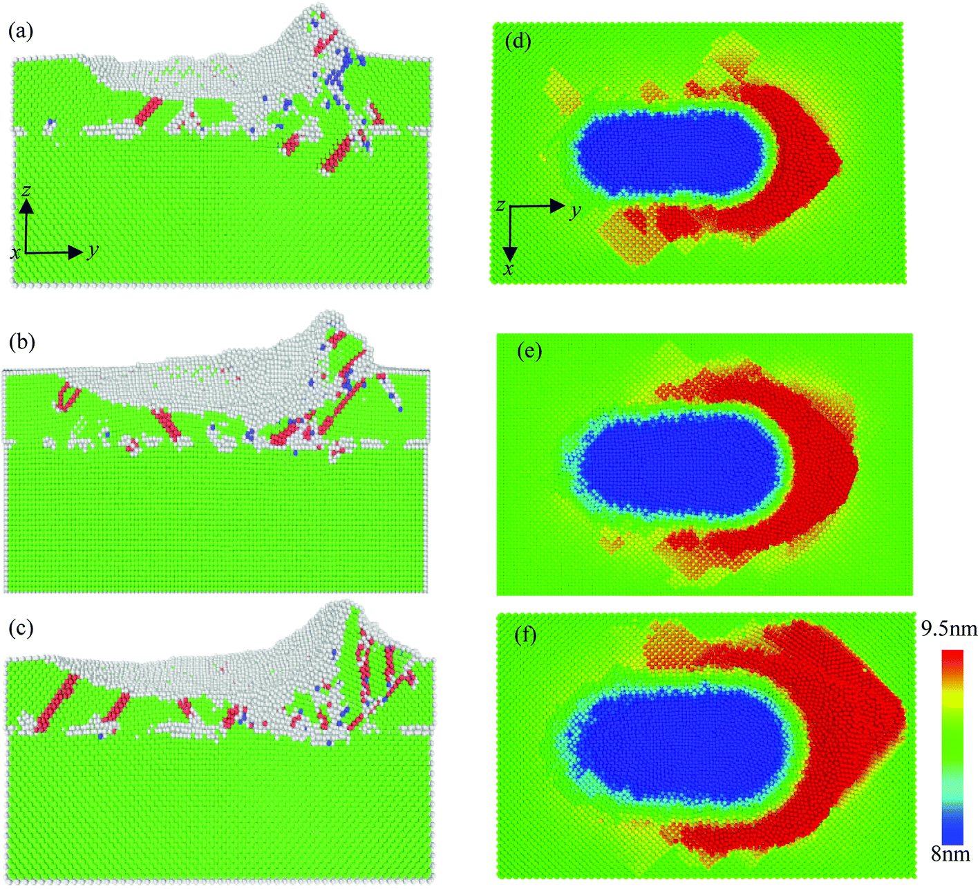 | ||
| Fig. 7 The instantaneous structure (a–c) and surface morphology (d–f) of the deformed Cu/Ag bilayers at different tool radii of (a and d) 3 nm, (b and e) 4 nm and (c and f) 5 nm. | ||
4.2. Effect of tool speed
According to the previous work,26 a general machining speed is less than 45 m s−1, a high machining speed of 45–150 m s−1, and a ultra-high machining speed is more than 150 m s−1. In order to investigate the effect of tool speed on the nanometric machining of Cu/Ag bilayers, three speeds of 20, 100, 200 m s−1 are selected in the simulations.Fig. 8a shows the evolution of the average temperature during the indenter penetrating into the Cu/Ag bilayers. It is found the temperature is affected slightly by the tool speed during nanoindentation process. The variation of indentation force versus indentation depth at different tool speeds is shown in Fig. 8b. As the lattice defects do not have sufficient time to recover or adjust and new lattice defects continue to form under the high-velocity nanoindentation, the Cu/Ag bilayers are strengthened. Therefore, the larger indentation force is needed for the indenter penetration and further plastic deformation at higher velocity. When the indentation depth is reached 1.5 nm, the nanoscratching is conducted. Fig. 8c shows the increased number of different types of atoms at machining speed of 100 m s−1. It is seen that the FCC atomic number decreases with the increment of ISF and other atoms (zone I and III), indicating that plastic deformation of Cu/Ag bilayers is dominated by the dislocation nucleation and propagation. In addition, zone II shows the different types of atom number fluctuate slightly, which can be ascribed to the interaction of dislocations. The dislocation intersection would restrict the dislocation motion, and lead to the hardening and lower plasticity. And some dislocations can be absorbed by mismatch dislocations of interface.17 Fig. 8d shows the evolution of different types of atom number versus machining distance during nanoscratching with different tool speeds. Due to the less time for the rearrangement of deformed atom lattices at high-velocity machining, more dislocation cores appear in Cu/Ag bilayers. Thus the number of ISF atoms displays little variation, but that of other atoms increases with the increment of tool speed.
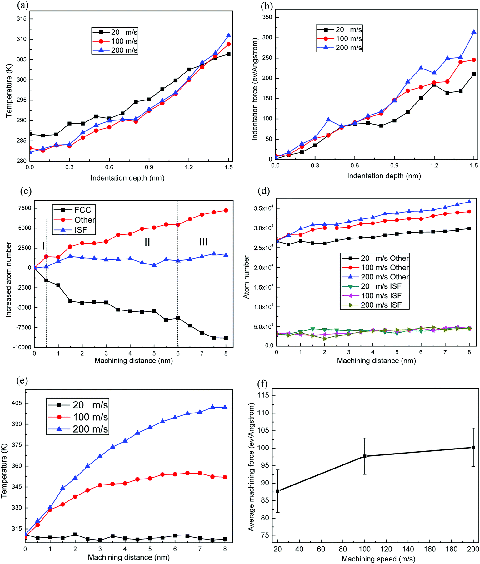 | ||
| Fig. 8 The relationship curves of the average temperature (a) and indentation force (b) versus indentation depth. The evolution curves of different types of atom numbers (c and d) and the average temperature (e) versus machining distance. The average machining forces (f) during stable machining processes of Cu/Ag bilayers with different machining speeds. The tool radius is 4 nm. | ||
Fig. 8e shows the evolution of the average temperature versus machining distances at different machining speeds. Under a higher machining speed, the friction between atoms is more drastic. Consequently more friction energy is released from the deformed crystal lattices and further transformed to the machining heat. The machining heat would diffuse toward the thermostat layer. Since the tool needs the less time to complete the same machining distance at a higher machining speed, thus the less time is provided to heat diffusion, which causes higher temperature for Cu/Ag bilayers in case of higher machining speed. In addition, due to the increment of heat dissipation rate as the tool advances, until the balance between heat dissipation rate and the heat production rate,26 the temperatures finally become steady, as shown in Fig. 8e.
Fig. 8f shows the average machining forces at different machining speeds, and the error bar represents the average error between the machining forces and the average machining force during stable machining process of Cu/Ag bilayers. The average machining force is larger at the higher machining speed, which involves with the dislocation generation events during the material removal process.56 Due to the lower machining speed than the propagation speed of a plastic wave, the dislocations propagate away from the tool–workpiece interaction region more easily and more dislocations nucleate under higher machining speed (Fig. 8d). This strengthens the Cu/Ag bilayers and larger machining force is needed for the high-speed advancement of tool.26
Fig. 9a–c display the surface morphology of Cu/Ag bilayers at different machining speed. In order to exhibit the chipping volume, the atoms are colored depending on atomic height. It is seen that machining speed has a significant influence on the volume of the chipping pileup. A comparison of Fig. 9a–c demonstrates that a larger volume of chippings appear under a higher machining speed. In addition, the quality of ground surface varies with the machining speed. The effect of machining speed on groove roughness is certified in Fig. 9d. The groove roughness is named as Rmax, which is the maximum height asperity of the groove area along the machining direction, and is the average distance between the highest point within the asperity and the lowest point within the groove.57 Fig. 9d describes that the increasing machining speed generates the increment of groove roughness, and the variation of the groove roughness to machining speed is more sensitive at a low speed. Based on above discussions, the selection of a low machining speed is beneficial to reduce the subsurface damage and improve the smoothness of ground surface during nanometric machining of Cu/Ag bilayers.
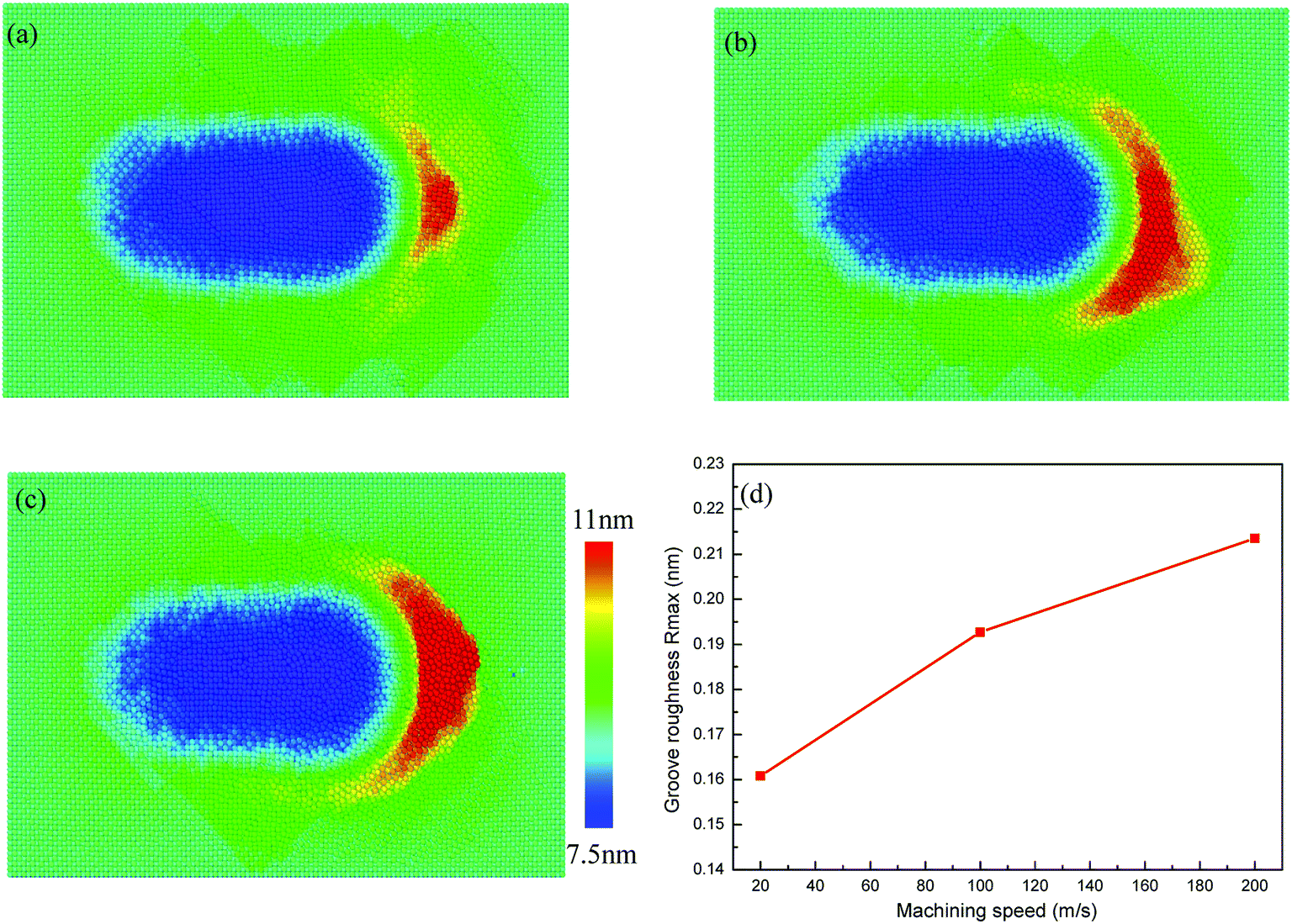 | ||
| Fig. 9 The surface morphology of Cu/Ag bilayers at different machining speeds: (a) 20 m s−1, (b) 100 m s−1, (c) 200 m s−1. The groove roughness at different machining speeds (d). The tool radius are 4 nm. Atoms are colored in accordance with atomic height in (a–c). | ||
4.3. Effect of machining depth
The machining depth hmax is maximum indentation depth achieved during the nanoindentation process, and the tool cuts workpiece at this depth in the nanometric machining process. Fig. 10 shows the instantaneous deformed structure and surface morphology of Cu/Ag bilayers at different machining depths of 1, 1.5 and 2.5 nm. Fig. 10a–c are the corresponding snapshot in x–y cross-section, where atoms are colored according to the CNA values. It can be seen from Fig. 10d–f the chipping volume at different machining depths, where atoms are colored according to atomic height. Under larger machining depth, more lattice defects are observed in machining zone (Fig. 10a–c). Correspondingly, more chippings are generated around the groove (Fig. 10d–f). When the machining depth is relatively larger, more atoms around the tool are extruded and emerge on the surface later, thereby more chippings pile up on the surface. Due to the existence of external stress field beneath the tool, the arrangement of Cu atoms in the tool–workpiece interaction zone sharply changes. As a result, the nucleation and slipping of partial dislocation along {111} slip planes dominate the plastic deformation of Cu/Ag bilayers during nanometric machining. | ||
| Fig. 10 The instantaneous structure (a–c) and surface morphology (d–f) of deformed Cu/Ag bilayers at different machining depths: (a and d) 1 nm, (b and e) 1.5 nm, and (c and f) 2.5 nm. The tool radius, machining speed and machining distance are 4 nm, 100 m s−1 and 6.5 nm, respectively. | ||
Fig. 11a describes the variation of machining force versus machining distances at different machining depths of 1, 1.5 and 2.5 nm. Since more lattice defects are induced by larger machining depth in the machining zone (Fig. 10a–c), the Cu/Ag bilayers is strengthened more severely and a larger machining force is required to keep cutting at the constant speed of 100 m s−1. The evolution of the average temperature versus machining distance is shown in Fig. 11b. There is higher initial temperature under larger machining depth for the nanoscratching of Cu/Ag bilayer, which is attribute to the effect of nanoindentation process. Namely, the larger indentation depth would inevitably cause the higher temperature during nanoindentation. In the following nanoscratching process, the average temperature evolution follows a similar rule with machining forces. The larger machining depth leads to higher temperature. Therefore, the smaller machining depth could reduce subsurface damage by relatively less ISF atoms, and decrease energy consumption by relatively low temperature.
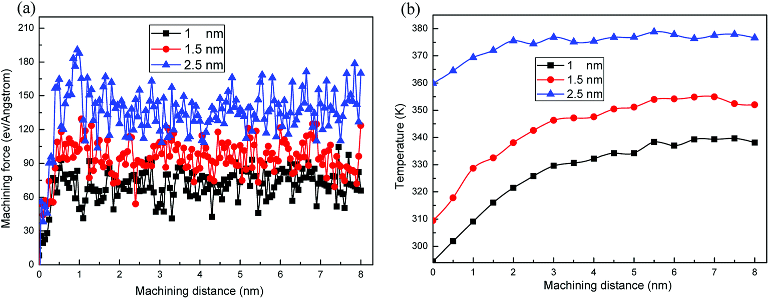 | ||
| Fig. 11 The variation curves of the machining force (a) and average temperature (b) versus machining distance at different machining depths in the Cu/Ag bilayers. The tool radius and machining speed are 4 nm and 100 m s−1. | ||
5. Conclusions
Three dimensional MD simulations of nanometric machining process on Cu/Ag bilayers and pure Cu film are conducted to study the mechanical and tribological properties of Cu/Ag bilayers. The effects of machining parameters on the subsurface damage and material removal of Cu/Ag bilayers are also investigated by changing the indenter radius, tool speed and machining depth during nanometric machining. Based on the above discussions, conclusions can be drawn as follows:(1) Due to the dislocation nucleation and emission from the Cu/Ag interface, the hardness of Cu/Ag bilayers is smaller than that of pure Cu film. The Cu/Ag bilayers have a larger friction coefficient than pure Cu film. In addition, the metal bonding energy in Cu/Ag interface is weaker than that in pure Cu film, which also induces the hardness of Cu/Ag bilayers to be smaller than that of pure Cu film. Young's modulus in Cu/Ag bilayers and pure Cu film is calculated by the Hertz contact mechanism and close to experiment result.
(2) Comparing different indenter radii, the chipping volume and the number of ISF atoms beneath the indenter increase with the increment of the indenter radius during nanometric machining of Cu/Ag bilayers. The larger indenter radius causes larger heat dissipation, thereby more defects are induced by thermal activation. Thus, a smaller indenter radius should be selected for the nanometric machining to reduce subsurface damage via relatively less ISF atoms and lower machining heat.
(3) The selection of lower tool speed is crucial to reduce the subsurface damage and improve the smoothness of ground surface. The higher tool speed would produce more chippings and larger groove roughness. Simultaneously, the high-speed machining needs to be maintained by the larger machining force. The higher temperature is caused by the higher tool speed and further induces more defects.
(4) With decrease of machining depth, the chipping volume and the number of defect atoms reduce sharply, resulting in the decreasing of subsurface damage at the smaller machining depth.
Conflicts of interest
There are no conflicts to declare.Acknowledgements
The authors would like to deeply appreciate the support from the Foundation for Innovative Research Groups of the National Natural Science Foundation of China (Grant No. 51621004), the NNSFC (11772122, 51871092, 51625404, 51771232, and 51671217), the Fundamental Research Funds for the Central Universities (531107051151), and the National Key Research and Development Program of China (2016YFB0700300).References
- Z. Zhang and H. M. Urbassek, J. Mater. Sci., 2018, 53, 799 CrossRef CAS.
- T. Fu, X. Peng, X. Chen, S. Weng, N. Hu, Q. Li and Z. Wang, Sci. Rep., 2016, 6, 35665 CrossRef CAS PubMed.
- Q. H. Fang, Q. Wang, J. Li, X. Zeng and Y. W. Liu, RSC Adv., 2017, 7, 42047 RSC.
- L. F. Zeng, R. Gao, Q. F. Fang, X. P. Wang, Z. M. Xie, S. Miao and T. Zhang, Acta Mater., 2016, 110, 341 CrossRef CAS.
- C. Zhang, K. Feng, Z. Li, F. Lu, J. Huang and Y. Wu, Appl. Surf. Sci., 2016, 378, 408 CrossRef CAS.
- C. Wang, J. M. Pureza, Y. Yang and Y. W. Chung, Surf. Coat. Technol., 2016, 288, 179 CrossRef CAS.
- B. Wang, Z. Zhang, K. Chang, J. Cui, A. Rosenkranz, J. Yu and N. Jiang, Nano Lett., 2018, 18, 4611 CrossRef CAS PubMed.
- A. Reserbat-Plantey, K. G. Schädler, L. Gaudreau, G. Navickaite, J. Güttinger, D. Chang and F. H. Koppens, Nat. Commun., 2016, 7, 10218 CrossRef CAS PubMed.
- J. J. Zhang, C. Begau, L. Geng and A. Hartmaier, Wear, 2015, 332, 941 CrossRef.
- S. Goel, X. Luo, A. Agrawal and R. L. Reuben, Diamond machining of silicon: a review of advances in molecular dynamics simulation, Int. J. Mach. Tools Manuf., 2015, 88, 131–164 CrossRef.
- L. Midolo, A. Schliesser and A. Fiore, Nat. Nanotechnol., 2018, 13, 11 CrossRef CAS PubMed.
- Z. Zhang, B. Wang, S. Huang, B. Wen, S. Yang, B. Zhang and D. Guo, Mater. Des., 2016, 106, 313 CrossRef CAS.
- D. D. Cui and L. C. Zhang, Adv. Manuf., 2017, 5, 20 CrossRef.
- J. J. Zhang, Z. F. Wang, T. Sun and Y. D. Yan, Mater. Res. Express, 2016, 3, 125018 CrossRef.
- B. Wang, Z. Zhang, J. Cui, N. Jiang, J. Lyu, G. Chen and F. Ye, ACS Appl. Mater. Interfaces, 2017, 9, 29451 CrossRef CAS PubMed.
- J. Li, Q. H. Fang, B. Liu and Y. W. Liu, Acta Mater., 2018, 147, 35 CrossRef CAS.
- C. Begau, A. Hartmaier, E. P. George and G. M. Pharr, Acta Mater., 2011, 59, 934 CrossRef CAS.
- H. Hertz, J. Reine Angew. Math., 1882, 92, 156 Search PubMed.
- S. Shao and S. N. Medyanik, Mech. Res. Commun., 2010, 37, 315 CrossRef.
- T. H. Fang and J. H. Wu, Comput. Mater. Sci., 2008, 43, 785 CrossRef CAS.
- D. Cheng, Z. J. Yan and L. Yan, Thin Solid Films, 2007, 515, 3698 CrossRef CAS.
- J. McKeown, A. Misra, H. Kung, R. G. Hoagland and M. Nastasi, Scr. Mater., 2002, 46, 593 CrossRef CAS.
- J. B. Liu, L. Zhang, D. W. Yao and L. Meng, Acta Mater., 2011, 59, 1191 CrossRef CAS.
- C. Zhao, X. Zuo, E. Wang, R. Niu and K. Han, Mater. Sci. Eng., A, 2016, 652, 296 CrossRef CAS.
- Y. Y. Tian, J. Li, Z. Y. Hu, Z. P. Wang and Q. H. Fang, Chin. Phys., 2017, 26, 162802 Search PubMed.
- J. Li, Q. H. Fang, Y. W. Liu and L. C. Zhang, Appl. Surf. Sci., 2014, 303, 331 CrossRef CAS.
- J. Stadler, R. Mikulla and H. R. Trebin, Int. J. Mod. Phys. C, 1997, 8, 1131 CrossRef.
- A. Stukowski, Modell. Simul. Mater. Sci. Eng., 2010, 18, 015012 CrossRef.
- J. D. Honeycutt and H. C. Andersen, J. Phys. Chem., 1987, 91, 4950 CrossRef CAS.
- T. Fu, X. H. Peng, Y. Zhao, B. C. Feng, C. Huang, Q. B. Li and Z. H. Wang, Appl. Phys. A, 2016, 122, 67 CrossRef.
- Y. Q. Geng, J. J. Zhang, Y. D. Yan, B. W. Yu, L. Geng and T. Sun, PLoS One, 2015, 10, 0131886 Search PubMed.
- S. Goel, X. Luo, A. Agrawal and R. L. Reuben, Int. J. Mach. Tools Manuf., 2015, 88, 131–164 CrossRef.
- Z. F. Wang, J. J. Zhang, H. ul Hassan, J. G. Zhang, Y. D. Yan, A. Hartmaier and T. Sun, Int. J. Mech. Sci., 2018, 148, 531–539 CrossRef.
- J. Li, Q. H. Fang, B. Liu, Y. W. Liu and Y. Liu, RSC Adv., 2016, 6, 76409 RSC.
- P. Peng, G. L. Liao, T. L. Shi, Z. R. Tang and Y. Gao, Appl. Surf. Sci., 2010, 256, 6284 CrossRef CAS.
- S. M. Foiles, M. I. Baskes and M. S. Daw, Phys. Rev. B, 1986, 33, 7983 CrossRef CAS.
- M. S. Daw, S. M. Foiles and M. I. Baskes, Mater. Sci. Rep., 1993, 9, 251 CrossRef CAS.
- H. Gercek, Int. J. Rock Mech. Min. Sci., 2007, 44, 1 CrossRef.
- M. Verdier, H. Huang, F. Spaepen, J. D. Embury and H. Kung, Philos. Mag., 2006, 86, 5009–5016 CrossRef CAS.
- S. I. Hong and M. A. Hill, Acta Mater., 1998, 46, 4111 CrossRef CAS.
- T. D. Shen, C. C. Koch, T. Y. Tsui and G. M. Pharr, J. Mater. Res., 1995, 10, 2892 CrossRef CAS.
- H. Zhao, C. Shi, P. Zhang, L. Zhang, H. Huang and J. Yan, Appl. Surf. Sci., 2012, 259, 66 CrossRef CAS.
- I. N. Sneddon, Int. J. Eng. Sci., 1965, 3, 47 CrossRef.
- A. C. Fischer-Cripps, Nanoindentation, New York, 2004, pp. 1–20 Search PubMed.
- C. Qiu, P. Zhu, F. Fang, D. Yuan and X. Shen, Appl. Surf. Sci., 2014, 305, 101 CrossRef CAS.
- D. Saraev and R. E. Miller, Acta Mater., 2006, 54, 33 CrossRef CAS.
- D. Beegan, S. Chowdhury and M. T. Laugier, Surf. Coat. Technol., 2005, 192, 57 CrossRef CAS.
- G. V. Gibbs, D. F. Cox and K. M. Rosso, J. Phys. Chem. A, 2004, 108, 7643 CrossRef CAS.
- D. J. González, L. E. González and M. J. Stott, Phys. Rev. Lett., 2004, 92, 085501 CrossRef PubMed.
- W. R. Chang, I. Etsion and D. B. Bogy, J. Tribol., 1988, 110, 57 CrossRef.
- L. Vitos, A. V. Ruban, H. L. Skriver and J. Kollar, Surf. Sci., 1998, 411, 186 CrossRef CAS.
- J. Li, Q. H. Fang, B. Liu and Y. W. Liu, Appl. Surf. Sci., 2016, 384, 419 CrossRef CAS.
- J. Li, Q. H. Fang, Y. W. Liu and L. C. Zhang, Int. J. Adv. Des. Manuf. Technol., 2015, 77, 1057 CrossRef.
- X. Zhu, H. Hou, X. Huang, M. Zhou and W. Wang, Constr. Build. Mater., 2012, 29, 476 CrossRef.
- G. Ziegenhain, H. M. Urbassek and A. Hartmaier, J. Appl. Phys., 2010, 107, 061807 CrossRef.
- Y. Liu, B. Z. Li and L. F. Kong, Comput. Mater. Sci., 2018, 148, 76 CrossRef CAS.
- F. Sun, S. Qu, Y. Pan, X. Li and C. Yang, Int. J. Adv. Des. Manuf. Technol., 2014, 73, 613 CrossRef.
| This journal is © The Royal Society of Chemistry 2019 |