
 Open Access Article
 This Open Access Article is licensed under a Creative Commons Attribution-Non Commercial 3.0 Unported Licence
Enhanced photoelectrochemical activity of Co-doped β-In2S3 nanoflakes as photoanodes for water splitting†
Supriya Pulipakaa,
A. K. S. Koushika,
Melepurath Deepa b and
Praveen Meduri*a
b and
Praveen Meduri*a
aDepartment of Chemical Engineering, Indian Institute of Technology Hyderabad, Kandi, Sangareddy-502285, Telangana, India. E-mail: meduripraveen@iith.ac.in
bDepartment of Chemistry, Indian Institute of Technology Hyderabad, Kandi, Sangareddy-502285, Telangana, India
First published on 11th January 2019
Abstract
This work is primarily focused on indium sulfide (β-In2S3) and cobalt (Co)-doped β-In2S3 nanoflakes as photoanodes for water oxidation. The incorporation of cobalt introduces new dopant energy levels increasing visible light absorption and leading to improved photo-activity. In addition, cobalt ion centers in β-In2S3 act as potential catalytic sites to promote electro-activity. 5 mol% Co-doped β-In2S3 nanoflakes when tested for photoelectrochemical water splitting exhibited a photocurrent density of 0.69 mA cm−2 at 1.23 V, much higher than that of pure β-In2S3.
Introduction
Photoelectrochemical (PEC) water splitting is attracting huge attention since solar energy is directly converted into hydrogen which can be used as fuel. A PEC semiconductor device in an aqueous electrolyte, irradiated with sunlight can directly split water into hydrogen and oxygen. The overall reaction in PEC is controlled by the oxygen evolution reaction (OER) at the anode due to its sluggish kinetics.1 Fujishima and Honda first reported a PEC device by using titania (TiO2) as a photoanode in 1972.2 However, TiO2 absorbs only 5% of the solar spectrum due to its large band gap of 3.2 eV and is primarily limited to the ultraviolet region. The requirement for visible light absorption drives the development of metal oxides with narrow band gap such as bismuth vanadate (BiVO4),3 tungsten oxide (WO3), and hematite (α-Fe2O3).4–6 Along with metal oxides, metal sulfides have garnered attention as promising materials due to their unique properties with good mechanical and thermal stability in electrochemical devices.7 Metal chalcogenides have received recent interest in photocatalysis owing to their narrow band gap and low-temperature synthesis.8 Among the metal chalcogenides, cadmium sulfide (CdS) with a band gap of 2.4 eV is a highly photoactive material under visible light. However, toxicity and photocorrosion make its use challenging for water oxidation.9–11 A recent study on multishelled hollow structures with CdS and zinc sulfide (ZnS) have shown enhanced PEC performance.12 The other chalcogenide which has a favorable band gap of 2.0–2.3 eV is indium sulfide (β-In2S3). It is a n-type semiconductor which is primarily used for solar cells with visible-light absorption.13–15 A variety of 2D β-In2S3 morphologies such as nanobelts and nanoflakes have been synthesized using metal ions such as calcium and aluminum to restrict the crystal growth in 2D wherein the nanoflakes have shown the best photoelectrochemical activity.16 A biomaterial template with amino acids has been used to synthesize high surface area β-In2S3 nanoflakes with increased number of surface active sites which are shown to promote the photocatalytic process of alcohol to aldehyde selective oxidation.17 However, the use of β-In2S3 nanoflakes for PEC water splitting to generate H2 or O2 has been sparsely reported despite good photocatalytic properties of β-In2S3.18,19 Previous studies have strived for the improvement of β-In2S3 photocatalytic properties by the way of heterojunctions with TiO2, MoS2, CdS and CuS.20–22 Alongside, noble metal nanoparticles such as silver have also been used to improve efficiency but at the expense of increased cell costs.23 The electro and photoactivity of β-In2S3 can be improved by doping with metals like zirconium,24 cobalt,25 tin26,27 and vanadium.28 The present work explores the introduction of a transition metal, cobalt (Co) into β-In2S3 nanoflakes by chemical bath deposition (CBD) at relatively low temperatures. The doping of Co has been confirmed by optical studies. Co-doped β-In2S3 showed an improved PEC activity due to an increase in the photo and electroactivity. To the best of our knowledge, there is only one report on Co-doped β-In2S3 which is an atomic layer confined doping in three stacked layers and used as photoanode for PEC water oxidation. They reported a current density of 1.17 mA cm−2 at an applied potential of 1.5 V (vs. RHE) in the basic electrolyte.25 Mesoporous TiO2 offers a robust support for the deposition of sensitizers in solar energy conversion applications. In particular, metal sulfides can be easily deposited onto TiO2 using a chemical bath because of good adhesion properties. The electronic communication between the sensitizer and TiO2 is also high due to the strong electron affinity of TiO2.29 The adhesion of β-In2S3 nanoparticles on to bare fluorine doped tin oxide (FTO) substrate is poor and does get peeled off during testing. TiO2 coating on FTO leads to even deposition of β-In2S3 with improved adhesion. The photogenerated electrons of β-In2S3 can easily transfer to the conduction band of TiO2 due to its proper band alignment, thus separating the photogenerated electron–hole pairs effectively. In the present work, all the doped and un-doped samples are deposited on TiO2 layer.Experimental
Chemicals
Indium chloride from Alfa Aesar; thioacetamide, ethyl cellulose and terpineol from Sigma Aldrich; titanium tetrachloride (TiCl4) and cobalt acetate tetrahydrate from Merck are used without further purification. TiO2 powder (P25) is obtained from Evonik. Deionized water with a resistivity of 18.2 Ω cm is obtained from a Millipore Direct-Q3 UV system. FTO substrates obtained from Pilkington are cleaned in soap solution, 30% HCl, twice distilled water, ethanol and acetone in that particular sequence prior to use.Preparation of electrodes
Fig. 1a depicts the fabrication of photoelectrodes. Fig. 1b shows the as-synthesized powders of β-In2S3 and Co-doped β-In2S3 nanoflakes with a difference in color indicating a change in the optical emission properties. The mol% that is referred to in the entire document represents added mol% in the solution. The actual wt% is calculated from energy dispersive spectroscopy (EDS) which is given in the Fig. S1 in ESI.†
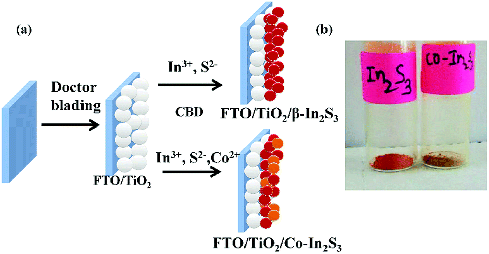 | ||
| Fig. 1 (a) Schematic representation of the synthesis process using CBD and (b) color difference between as-synthesized β-In2S3 and Co-doped β-In2S3. | ||
Characterization
XRD graphs of the samples are obtained on a PANalytical X'PertPRO instrument with Cu-Kα (λ = 1.5406 Å) radiation. HRTEM (High Resolution Transmission Electron Microscopy) images of β-In2S3 and Co-doped β-In2S3 samples are obtained on a HRTEM JEOL JEM 2100 with a LaB6 filament operating at 200 kV. The samples are prepared by dispersing the powder in ethanol followed by ultrasonication for 1 hour before drop casting onto a carbon-coated copper grid. The solvent is evaporated and further used as a specimen for TEM. The optical absorption spectra of the films are measured in the diffuse reflectance mode and converted to absorbance using Kubelka–Munk function on a UV-Vis-NIR spectrophotometer (Shimadzu UV-3600). Raman spectra of the samples are recorded on a Bruker Senterra Dispersive Raman Microscope spectrometer. The laser excitation wavelength is fixed at 532 nm. Photoluminescence (PL) spectra of films are measured on a Horiba Flouromax-4 fluorescence spectrometer; a suitable filter is utilized during the measurement and background correction is applied. Surface morphology analysis is performed using a field emission scanning electron microscope (Carl Zeiss Supra 40 FE-SEM). The specific surface area is calculated from N2 adsorption–desorption isotherms measured using a Micromeritics ASAP 2020 instrument using the Brunauer–Emmett–Teller (BET) method. Pore volume and pore-size distribution are calculated by using the Barrett–Joyner–Halenda (BJH) method.Photoelectrochemical performances
Photoelectrochemical data is studied using Autolab PGSTAT 302N equipped with NOVA 1.11 software. The light source is a white LED (40 W) and the intensity of the light is adjusted to 1 sun by keeping the optimum distance between the light and the sample. Light intensities are measured with a LOT-Oriel radiometer-photometer (ILT: 1400). A three electrode cell with the prepared β-In2S3 (or) Co-doped β-In2S3 samples as working electrode, a platinum wire as the counter electrode and Ag/AgCl as the reference electrode is used. 0.5 M Na2SO4 (buffered to pH = 7) is used as an electrolyte for all the measurements. The measured Ag/AgCl reference electrode potentials are converted to reversible hydrogen electrode (RHE) by using Nernst equation ERHE = EAg/AgCl + 0.0591 pH + 0.199 V. The photocurrent is measured by linear sweep voltammetry in the range of 0 to 1.6 V vs. RHE at a scan rate of 10 mV s−1. The time dependent currents are measured at a bias potential of 1.23 V vs. RHE. Prior to all the measurements argon gas is purged for 30 min to remove the dissolved oxygen in the solution.Results and discussion
XRD patterns of as-synthesized samples are shown in Fig. 2a. Peaks for TiO2 correspond to the body-centered tetragonal structure of TiO2 (PDF: 894921). The diffraction patterns in the range of 10–90° can be indexed as cubic phase β-In2S3 structure (PDF: 650459). The diffraction peak of β-In2S3 at 2θ = 33.45° can be prominently seen which is indexed to (400) plane of β-In2S3 and the other peaks overlap with TiO2. Fig. 2b shows the XRD peaks without TiO2. No distinct characteristic peaks are visible in XRD of the doped samples which rules out the formation of a new compound, potentially cobalt sulfide (CoS2). The broadened peaks do indicate that the as-synthesized samples consist of nanomaterials i.e. nanoflakes in this case. The β-In2S3 crystal has a defect spinel lattice structure; there are twelve tetrahedral sites in β-In2S3 of which eight are occupied by In3+ ion whereas four are empty. These empty sites can be potentially occupied by other metals,30 paving ways for doping of metals in β-In2S3 at synthesis temperatures of β-In2S3 i.e., low temperatures. Cobalt-doped in our study is believed to occupy one or more empty tetrahedral sites of β-In2S3 which is confirmed by optical studies and discussed a little later. We observe a shift of 0.1° for the (400) plane in the doped sample and the crystallite size decreases with increasing Co2+ ion concentration in doped samples. The smaller size of Co2+ ion (70 pm) in comparison to the In3+ ion (80 pm) occupying the empty tetrahedral sites and binding to the other elements in the crystal causes a reduction in the overall crystallite size of the material. The average crystallite sizes of β-In2S3, Co-doped β-In2S3 with 2, 5 and 8 mol% are 9.22 nm, 9.2 nm, 8.08 nm, and 7.77 nm respectively. Fig. 2c shows the UV-Vis-NIR diffuse reflectance spectra for both doped and undoped samples. The undoped β-In2S3 nanoflakes have an absorption peak at 650 nm which correlates to a band gap of 1.9 eV. The doped samples have three sub-bandgap absorption peaks in the range of 650–900 nm corresponding to new energy levels in addition to the absorption peak at 650 nm. The position of the β-In2S3 absorption peak in the visible region did not alter with the doping level. The three peaks seem to overlay against each other and appear as one broad peak.16 The broad peak is indicative of the tetrahedrally coordinated Co2+ ion transitions, 2E(G) → 4A2(F), 4T1(P) → 4A2(F), 2A1(G) → 4A2(F) respectively.25 The twelve In3+ sites in the spinel β-In2S3 structure have tetrahedral coordination while there is no tetrahedral Co2+ co-ordination in CoS2 (cubic pyrite structure). Hence, the broad peak above indicates that Co2+ ions are located at tetrahedral sites in β-In2S3 which is indicative of doping.31,32 The incorporation of Co2+ ion in the vacant sites does improve photoabsorption. Cobalt sites in β-In2S3 can act as trapping sites for the photogenerated electrons/holes which will prevent their recombination.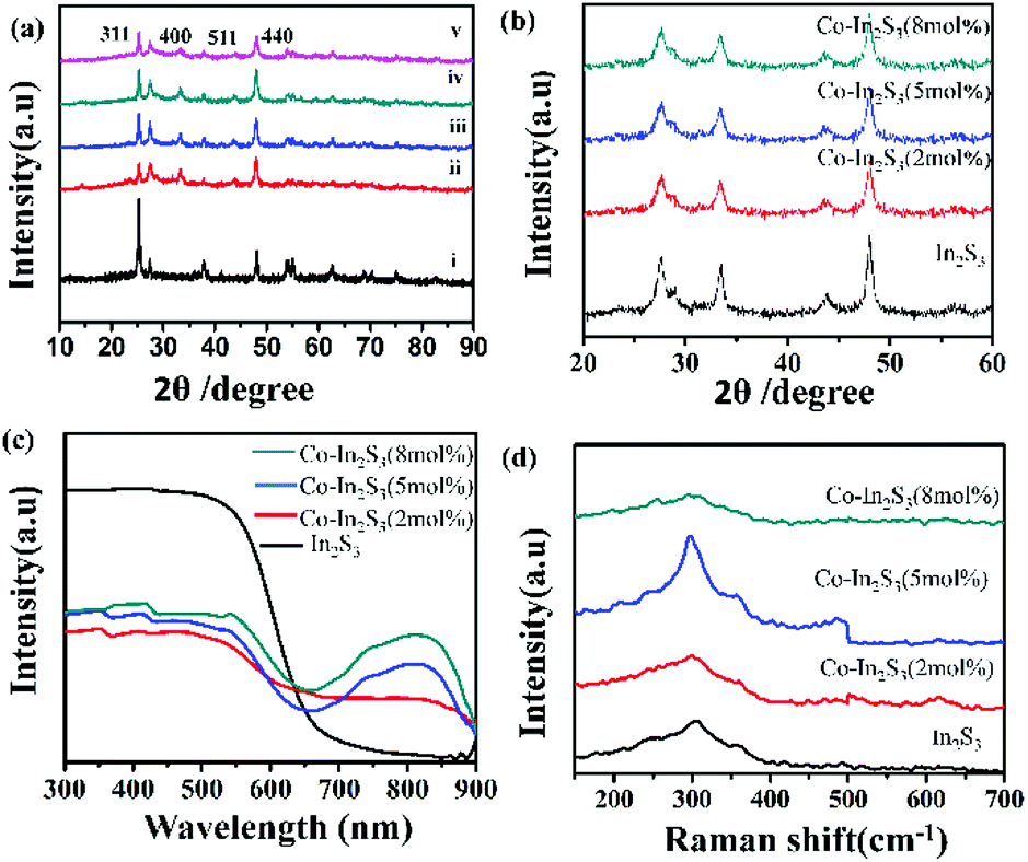 | ||
| Fig. 2 (a) X-ray diffraction pattern of (i) TiO2 (ii) TiO2/β-In2S3 (iii) (iv) and (v) TiO2/Co-doped β-In2S3 with 2, 5, 8 mol% respectively (b) X-ray diffraction pattern without TiO2 (c) UV-Vis-NIR diffuse reflectance spectra (d) Raman spectra. | ||
Raman spectra in Fig. 2d shows a characteristic peak at 305 cm−1 which pertains to A1g mode confirming the structure and phase of β-In2S3 nanoflakes.33 This peak is ascribed to symmetric stretching of the vibrating mode in InS4 tetrahedra. Fig. 2d shows a considerable shift from 305 cm−1 to 297.7 cm−1 when β-In2S3 is doped with cobalt. The incorporation of Co2+ ions in the tetrahedral sites and binding to other elements (sulfur) can lead to bond stretching of In–S which is seen as a blueshift in the observed spectra. Furthermore, only a slight shift from 297.7 cm−1 to 296.3 cm−1 is observed when the Co mol% is increased in the sample. It shows that once bond stretching happens, further addition of Co2+ does not alter the binding to sulfur which is indicative of Co2+ doping rather than formation of CoS2. In addition, it also indicates the saturation of Co2+ ions in the β-In2S3 structure beyond a certain concentration which is reflected in the electrochemical data.
SEM images in Fig. 3a and b show the agglomerated particles of β-In2S3 and Co-doped β-In2S3 deposited on TiO2 respectively. These uniform microspheres have an average size of 1–1.5 μm in both the doped and undoped samples. These microspheres consist of bundles of nanoflakes as shown in TEM images. Fig. 3c and d show nanoflakes of 5 mol% Co-doped β-In2S3 which are of 20–30 nm width and 40–50 nm length. These small nanoflakes tend to collate during stirring in the CBD process which leads to the formation of microspheres or nanoflowers.22,33
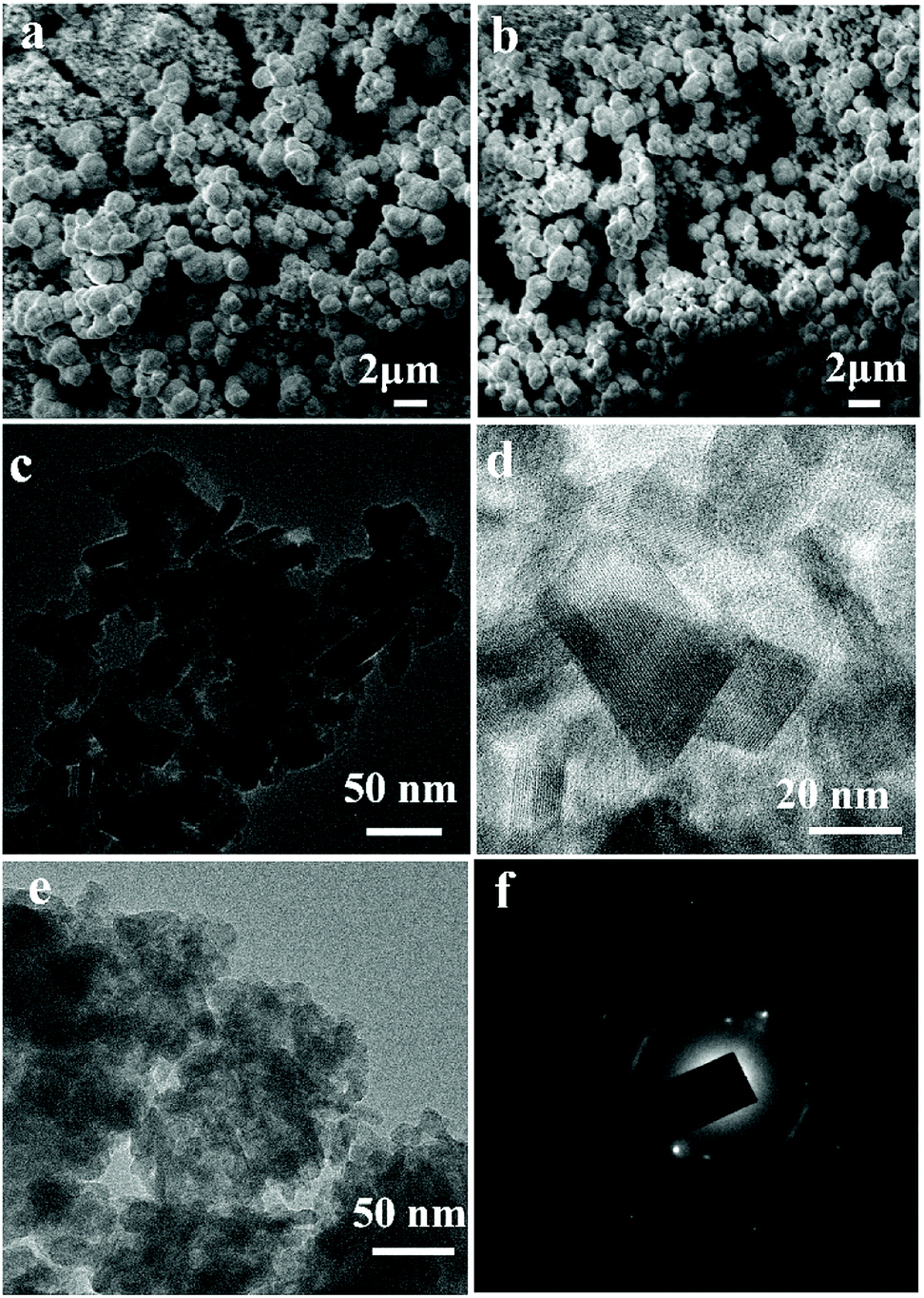 | ||
| Fig. 3 SEM images of (a) TiO2/β-In2S3 and (b) TiO2/Co-doped β-In2S3 (5 mol%). TEM images of (c) 5 mol% Co-doped β-In2S3 with clearly visible nanoflakes (d) individual nanoflake of 5 mol% Co-doped β-In2S3 (e) nanoflakes of 8 mol% Co-doped β-In2S3 and (f) SAED pattern of 8 mol% Co-doped β-In2S3 indicating crystallinity. | ||
In order to confirm the presence of Co doping in β-In2S3, Energy Dispersive Spectroscopy (EDS) analysis and elemental mapping studies have been carried out. Fig. 4a shows the SEM image of TiO2/Co-doped β-In2S3. The cross-sectional view of the TiO2/Co-doped β-In2S3 film in Fig. 4b shows homogenous and well-integrated layers which lead to low recombination losses.34 Owing to the porosity of TiO2 layer, Co-doped β-In2S3 nanoparticles easily percolate through and coat the TiO2 particles. Thus, the resulting TiO2/Co-doped β-In2S3 film appears as a single homogeneous entity and the thickness of the film is inferred to be nearly 8.10 μm. Fig. 4c–e show the elemental mapping of 5 mol% Co-doped β-In2S3. Fig. 4e clearly demonstrates the uniform distribution of cobalt in the β-In2S3 crystal structure. Line scan of an individual Co-doped β-In2S3 particle also confirms the uniform distribution of cobalt in the particle which is shown in ESI (Fig. S1).†
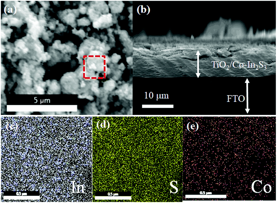 | ||
| Fig. 4 SEM images of (a) TiO2/Co-doped β-In2S3 (b) cross sectional view of TiO2/Co-doped β-In2S3 film and (c–e) EDS elemental mapping of selected area of inset in (a). | ||
The specific surface area and porosity are calculated by N2 adsorption–desorption isotherms (Fig. 5b). Both the isotherms are identified as type IV with a hysteresis loop which is a characteristic of mesoporous materials. Mesopores primarily arise due to the spaces between the nanoflakes in the microspheres.35 The BET surface area of the β-In2S3 and 5 mol% Co-doped β-In2S3 are estimated to be 52.17 m2 g−1 and 101.15 m2 g−1, respectively. The doping of Co does increase specific surface area significantly. The values are reported in ESI (Table 1).† Generally, doping is believed to inhibit the particle growth and lead to an increase in the specific surface area. The as-prepared Co-doped β-In2S3 showed a higher specific surface area than most of the reported values.36 High surface area can provide more active sites for the adsorption of reactants on the surface which improves interfacial charge transfer thus improving the photocatalytic properties.
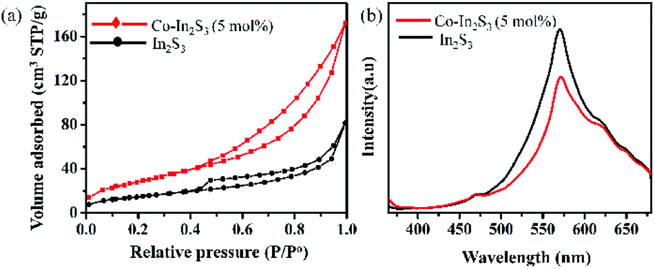 | ||
| Fig. 5 Comparison of TiO2/β-In2S3 and TiO2/Co-doped β-In2S3 (5 mol%) properties using (a) nitrogen adsorption–desorption isotherms and (b) photoluminescence (PL) spectra. | ||
Photoluminescence data presented here indicates the recombination intensity. Lower PL intensity indicates less recombination of photo-induced electron–hole pairs, and higher photocatalytic activity.27,37 Fig. 5b shows the PL spectra of both pure β-In2S3 and 5 mol% Co-doped β-In2S3. PL quenching is shown at an excitation wavelength of 350 nm. 5 mol% Co-doped β-In2S3 displays significantly diminished intensity as compared to pure β-In2S3 which is indicative of the efficient charge separation of photogenerated electron–hole pairs and lower recombination. Improved efficiency is due to Co doping which delayed the recombination rate of photogenerated charge carriers of β-In2S3.
Fig. 6a shows the schematic of 3-electrode setup where the electron transfer mechanism is explained. The photogenerated electrons under irradiation move from β-In2S3 to TiO2 due to their proper band alignment. The holes in β-In2S3 help in water oxidation. Photoanode studies are generally carried out in basic medium as oxygen evolution is higher with high hydroxide ion concentration. Even though the currents are high, extreme pH conditions will damage other parts of the cell with prolonged use leading to maintenance and safety issues in practical applications.38 Therefore, we use neutral pH solution for all our testing purposes unless indicated otherwise. Fig. 6b shows linear sweep voltammograms (LSV) of the β-In2S3, Co-doped β-In2S3 electrodes in Argon gas purged 0.5 M Na2SO4 (pH = 7) under light and dark conditions. All the electrodes showed negligible current in the potential range of 0 to 1.6 V vs. RHE under dark conditions. Current densities are reported at a potential of 1.23 V vs. RHE. The photocurrent density of pure β-In2S3 is 0.32 mA cm−2. The photocurrent densities of 2, 5 and 8 mol% Co-doped β-In2S3 are 0.37, 0.69 and 0.46 mA cm−2 respectively. The photoanodes exhibited an onset potential of 0.14 V vs. RHE which is quite low in comparison to the literature reported values.24 The low onset potential indicates good charge carrier separation and transport in the photoanode. Among all the doped samples, 5 mol% Co-doped β-In2S3 shows the best performance with double the current density of pure β-In2S3. Particularly, Co2+ ions in β-In2S3 nanoflakes act as trapping sites for the photogenerated electrons which will prevent the recombination of electron–hole pairs and lead to enhancement of photoactivity. It leads to higher density of charge carriers. As cobalt is a transition metal with well-known electroactivity,25,39,40 it also acts as an active site for the promotion of water oxidation reaction. Hence doped β-In2S3 leads to the enhancement of both photo and electro activity. However, the increase in cobalt concentration beyond 5 mol% does not increase the current density. The probable cause for this is that the low temperatures limit the diffusion of cobalt ion inside the material but rather deposit on the surface beyond a certain concentration. Hence, the activity goes down after 5 mol% doping of cobalt.
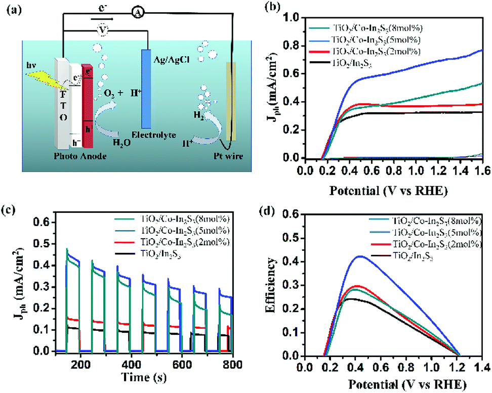 | ||
| Fig. 6 Photoelectrochemical properties of TiO2/β-In2S3, TiO2/Co-doped β-In2S3 with 2, 5 and 8 mol%. (a) Three electrode measurement setup (b) linear sweep voltammograms in light and dark conditions (c) chrono-amperometry curves under chopped light at 1.23 V vs. RHE and (d) photoconversion efficiency of all samples. | ||
Fig. 6c shows chronoamperometry (CA) curves of all the synthesized electrodes under chopped light at 1.23 V vs. RHE. High and stable photocurrent density is obtained for 5 mol% Co-doped β-In2S3 when compared to other electrodes. Fig. 6d shows the solar to hydrogen (STH) conversion efficiency curves as a function of the applied voltage, which is calculated using the equation
5 mol% Co-doped β-In2S3 achieves the highest efficiency of 0.42% at 0.42 V, which is double than pure β-In2S3 (0.24% at 0.37 V). However, the onset potentials of all the electrodes are the same suggesting no occurrence of compositional and structural modification by introduction of cobalt. We also analyzed the samples as well as electrolyte after water oxidation for a span of 1 h. The electrolyte after prolonged illumination is mixed with thioacetamide and heated to 80 °C for 2 h under stirring to check for indium dissolution. There is no change in the color of the electrolyte, which is indicative of no indium dissolution. In addition, we analyzed the TEM images before and after testing which are shown in Fig. 7. The d-spacing of (311) plane in Co-doped β-In2S3 is 0.32 nm. Co-doped β-In2S3 samples analyzed using TEM show no change in the d-spacing even after testing indicating no structural transformation to indium oxide. This shows that indeed, the stability of the Co-doped β-In2S3 is good and have a strong potential to be used practically.
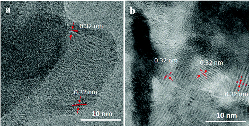 | ||
| Fig. 7 TEM images of (a) 5 mol% Co-doped β-In2S3 before testing and (b) TiO2/Co-doped β-In2S3 (5 mol%) after testing. | ||
Conclusions
In summary, Co-doped β-In2S3 nanoflakes are synthesized using chemical bath deposition at relatively low temperatures. 5 mol% Co-doped β-In2S3 nanoflakes with a current density of 0.69 mA cm−2 at 1.23 V vs. RHE and onset potential of 0.14 V vs. RHE showed superior performance in comparison to pure β-In2S3. In addition, it can be seen that the Co-doped β-In2S3 samples are stable in the neutral electrolyte.Conflicts of interest
There are no conflicts to declare.Acknowledgements
We would like to thank Indian Institute of Technology, Hyderabad for the financial support (seed grant no: SG/IITH/F148/2016-17/SG-6) in providing the necessary research facilities. We would also like to thank the TEM and XRD facilities in the institute for their help.Notes and references
- E. Fabbri, A. Habereder, E. Waltar, R. Kotz and R. J. Schmidt, Catal. Sci. Technol., 2014, 4, 3800–3821 RSC.
- A. Fujishima and K. Honda, Nature, 1972, 238, 37–38 CrossRef CAS.
- R. A. He, S. W. Cao and J. G. Yu, Acta Phys.-Chim. Sin., 2016, 32, 2841–2870 CAS.
- K. Sivula, F. Le Formal and M. Gratzel, ChemSusChem, 2011, 4, 432–449 CrossRef CAS PubMed.
- S. V. Kershaw, A. S. Susha and A. L. Rogach, Chem. Soc. Rev., 2013, 42, 3033–3087 RSC.
- P. Zhang, L. Yu and X. W. Lou, Angew. Chem., Int. Ed., 2018, 57, 15076–15080 CrossRef CAS PubMed.
- P. Kulkarni, S. K. Nataraj, R. G. Balakrishna, D. H. Nagaraju and M. V. Reddy, J. Mater. Chem. A, 2017, 5, 22040–22094 RSC.
- W. Sheng, Y. Song, M. Dou, J. Ji and F. Wang, Appl. Surf. Sci., 2018, 436, 613–623 CrossRef CAS.
- Z. Sun, Q. Yue, J. Li, J. Xu, H. Zheng and P. Du, J. Mater. Chem. A, 2015, 3, 10243–10247 RSC.
- M. Nguyen, P. D. Tran, S. S. Pramana, R. L. Lee, S. K. Batabyal, N. Mathews and M. Graetzel, Nanoscale, 2013, 5, 1479–1482 RSC.
- J. Zhang, Z. Zhu, Y. Tang, K. Mullen and X. Feng, Adv. Mater., 2014, 26, 734–738 CrossRef CAS PubMed.
- P. Zhang, B. Y. Guan, L. Yu and X. W. Lou, Chem, 2018, 4, 162–173 CAS.
- H. Jia, W. He, X. Chen, Y. Lei and Z. Zheng, J. Mater. Chem. A, 2011, 21, 12824–12828 RSC.
- J. Kim, H. Hiroi, T. K Todorov, O. Gunawan, M. Kuwahara, T. Gokmen, D. Nair, M. Hopstaken, B. Shin, Y. S. Lee and W. Wang, Adv. Mater., 2014, 26, 7427–7431 CrossRef CAS.
- S. K. Sarkar, J. Y. Kim, D. N. Goldstein, N. R. Neale, K. Zhu, C. M. Elliott, A. J. Frank and S. M. George, J. Phys. Chem. C, 2010, 114, 8032–8039 CrossRef CAS.
- Y. Tian, L. Wang, H. Tang and W. Zhou, J. Mater. Chem. A, 2015, 3, 11294–11301 RSC.
- T. Li, S. Zhang, S. Meng, X. Ye, X. Fu and S. Chen, RSC Adv., 2017, 7, 6457–6466 RSC.
- F. Jiang, T. Harada, Y. Kuang, T. Minegishi, K. Domen and S. Ikeda, J. Am. Chem. Soc., 2015, 137, 13691–13697 CrossRef CAS PubMed.
- M. Q. Yang, B. Weng and Y. J. Xu, Nano Res., 2013, 29, 10549–10558 CAS.
- J. Y. Do, R. K. Chava, S. K. Kim, K. Nahm, N. K. Park, J. P. Hong, S. J. Lee and M. Kang, Appl. Surf. Sci., 2018, 451, 86–98 CrossRef CAS.
- B. Sun, F. Shan, X. Jiang, J. Ji and F. Wang, Appl. Surf. Sci., 2018, 435, 822–831 CrossRef CAS.
- C. Gao, J. Li, Z. Shan, F. Huang and H. Shen, Mater. Chem. Phys., 2010, 122, 183–187 CrossRef CAS.
- R. Xu, H. Li, W. Zhang, Z. Yang, G. Liu, Z. Xu, H. Shao and G. Qiao, Phys. Chem. Chem. Phys., 2016, 18, 2710–2717 RSC.
- L. Wang, L. Xia, Y. Wu and Y. Tian, ACS Sustainable Chem. Eng., 2016, 4, 2606–2614 CrossRef CAS.
- F. Lei, L. Zhang, Y. Sun, L. Liang, K. Liu, J. Xu, Q. Zhang, B. Pan, Y. Luo and Y. Xie, Angew. Chem., Int. Ed., 2015, 54, 9266–9270 CrossRef CAS PubMed.
- M. Kilani, C. Guasch, M. Castagne and N. Kamoun-Turki, J. Mater. Sci., 2012, 47, 3198–3203 CrossRef CAS.
- J. Feng, Z. Yang, S. He, X. Niu, T. Zhang, A. Ding, H. Liang and X. Feng, Chemosphere, 2018, 212, 114–123 CrossRef CAS PubMed.
- C. Tapia, S. P. Berglund, D. Friedrich, T. Dittrich, P. Bogdanoff, Y. Liu, S. Levcenko, T. Unold, J. C. Conesa, A. L. De Lacey and M. Pita, J. Phys. Chem. C, 2016, 120, 28753–28761 CrossRef CAS.
- J. Piris, A. J. Ferguson, J. L. Blackburn, A. G. Norman, G. Rumbles, D. C. Selmarten and N. Kopidakis, J. Phys. Chem. C, 2008, 112, 7742–7749 CrossRef CAS.
- Z. Zheng, J. Yu, S. Cheng, Y. Lai, Q. Zheng and D. Pan, J. Mater. Sci.: Mater. Electron., 2016, 27, 5810–5817 CrossRef CAS.
- Y. Lu, Y. Lin, D. Wang, L. Wang, T. Xie and T. Jiang, Nano Res., 2011, 11, 1144–1152 CrossRef.
- R. He, B. Tang, C. Ton-That, M. Phillips and T. Tsuzuki, J. Nanopart. Res., 2013, 15, 2030 CrossRef.
- A. K. Nayak, S. Lee, Y. Sohn and D. Pradhan, CrystEngComm, 2014, 16, 8064–8072 RSC.
- O. Niitsoo, S. K. Sarkar, C. Pejoux, S. Rühle, D. Cahen and G. Hodes, J. Photochem. Photobiol., A, 2006, 181, 306–313 CrossRef CAS.
- C. Wei, W. Guo, J. Yang, H. Fan, J. Zhang and W. Zheng, RSC Adv., 2014, 4, 50456–50463 RSC.
- Y. Cheng, H. Niu, J. Chen, J. Song, C. Mao, S. Zhang and Y. Gao, J. Nanopart. Res., 2017, 19(5), 166 CrossRef.
- J. Liqiang, Q. Yichun, W. Baiqi, L. Shudan, J. Baojiang, Y. Libin, F. Wei, F. Honggang and S. Jiazhong, Sol. Energy Mater. Sol. Cells, 2006, 90, 1773–1787 CrossRef.
- S. Y. Chae, P. Sudhagar, A. Fujishima, Y. J. Hwang and O. S. Joo, Phys. Chem. Chem. Phys., 2015, 17, 7714–7719 RSC.
- A. Kaushik, B. Dalela, S. Kumar, P. A. Alvi and S. Dalela, J. Alloys Compd., 2013, 552, 274–278 CrossRef CAS.
- C. Bi, L. Pan, M. Xu, J. Yin, Z. Guo, L. Qin, H. Zhu and J. Q. Xiao, Chem. Phys. Lett., 2009, 481, 220–223 CrossRef CAS.
Footnote |
| † Electronic supplementary information (ESI) available. See DOI: 10.1039/c8ra09660k |
| This journal is © The Royal Society of Chemistry 2019 |