
 Open Access Article
 This Open Access Article is licensed under a Creative Commons Attribution-Non Commercial 3.0 Unported Licence
Suppression of GeOx interfacial layer and enhancement of the electrical performance of the high-K gate stack by the atomic-layer-deposited AlN buffer layer on Ge metal-oxide-semiconductor devices
Chin-I. Wang a,
Teng-Jan Changa,
Chun-Yuan Wanga,
Yu-Tung Yina,
Jing-Jong Shyueb,
Hsin-Chih Lina and
Miin-Jang Chen*a
a,
Teng-Jan Changa,
Chun-Yuan Wanga,
Yu-Tung Yina,
Jing-Jong Shyueb,
Hsin-Chih Lina and
Miin-Jang Chen*a
aDepartment of Materials Science and Engineering, National Taiwan University, Taipei, Taiwan. E-mail: mjchen@ntu.edu.tw
bResearch Center for Applied Science, Academia Sinica, Taipei, Taiwan
First published on 2nd January 2019
Abstract
For high-performance nanoscale Ge-based transistors, one important point of focus is interfacial germanium oxide (GeOx), which is thermodynamically unstable and easily desorbed. In this study, an atomic-layer-deposited AlN buffer layer was introduced between the crystalline ZrO2 high-K gate dielectrics and epitaxial Ge, in order to reduce the formation of interfacial GeOx. The results of X-ray photoelectron spectroscopy and high-resolution transmission electron microscopy demonstrate that the AlN buffer layer suppressed the formation of interfacial GeOx. Hence, significant enhancement of the electrical characteristics of Ge metal-oxide-semiconductor (MOS) capacitors was achieved with a two-orders-of-magnitude reduction in the gate leakage current, a 34% enhancement of the MOS capacitance, and a lower interfacial state density. The results indicate that the AlN buffer layer is effective in providing a high-quality interface to improve the electrical performance of advanced Ge MOS devices.
1. Introduction
Over the last decade, it has become increasingly difficult to improve the performance of silicon (Si) metal-oxide-semiconductor (MOS) field-effect transistors (FETs) via conventional device scaling. Due to high carrier mobility, germanium (Ge) and III–V compound MOSFETs have been regarded as very promising candidates for the further improvement of device performance and scaling.1–4 However, the lack of high-quality and thermodynamically stable gate dielectrics is a major problem in implementing Ge and III–V semiconductors as the channel materials.5–10 For Ge, it is difficult to suppress the formation of a low-K germanium oxide (GeOx) interfacial layer (IL) at the high-K and Ge interface, which limits the minimum achievable equivalent oxide thickness.11,12 In contrast to the SiO2/Si system, interfacial GeOx has been reported to be thermodynamically unstable.5 The smaller conduction band offset at the GeOx/Ge interface also results in an increase in the gate leakage current.13 Therefore, it is essential to prevent the formation of interfacial GeOx in high-performance Ge-based MOSFETs.13,14Many methods have been used to passivate the defects and achieve a stable high-K/Ge interface, such as the use of ultrathin Si, high-quality Ge oxides, and rare-earth oxides (Y2O3, SmGeOx, etc.).6,15–17 One of the most widely used methods is the insertion of an Al2O3 buffer layer between the high-K oxide and Ge because of the high bandgap and good thermal stability of Al2O3.18,19 Besides, it has been reported that nitrogen incorporation into GeOx yields an improvement in the thermal stability and the dielectric constant.20,21 However, an unstable GeOx is usually formed at the Al2O3/Ge and Ge-oxynitride/Ge interfaces. Furthermore, the use of germanium nitride (Ge3N4 or GeNx) as the gate dielectric and the buffer layer has been demonstrated to exhibit well-behaved capacitance–voltage characteristics.22–25 This improvement in the electrical performance may be the result of the suppression of interfacial GeOx because the preparation of the nitride does not involve the use of oxygen.
AlN is a good material for gate dielectrics and buffer layers because it has a higher dielectric constant than GeOx, good chemical stability, and a wide bandgap of ∼6.2 eV.26–28 AlN thin films are conventionally prepared by chemical vapor deposition (CVD) and sputtering.29,30 However, the typical deposition temperature for AlN prepared using CVD is greater than 700 °C,31 which is unfavorable for the integration of semiconductor processing. Besides, it is difficult to deposit high-quality nanoscale thin films using sputtering.32 Recently, atomic layer deposition (ALD) has been reported for the preparation of high-quality nanoscale AlN thin films at low temperatures.26,31 In this paper, remote plasma ALD (RP-ALD) was used to deposit a nanoscale AlN buffer layer between the crystalline ZrO2 high-K gate dielectrics and Ge. The interfacial GeOx was suppressed by the AlN buffer layer, so the capacitance equivalent thickness (CET), the interfacial state density (Dit) and the gate leakage current (Jg) of Ge MOS capacitors were significantly improved.
2. Experiments
The gate stacks in MOS capacitors are plotted schematically in Fig. 1. A Ge epitaxial layer was grown by remote plasma chemical vapor deposition using GeH4 at 375 °C on a highly-doped (0.001–0.003 Ω cm) n-type Si substrate. After pre-cleaning, the samples were immersed in dilute HF (1 min) and then rinsed with de-ionized water (30 s) for several cycles, in order to remove the native oxide on the Ge. The gate stacks, which were composed of ZrO2, Al2O3/ZrO2, and AlN/ZrO2, were then immediately deposited by RP-ALD (Fiji, Ultratech) at 250 °C. Tetrakis(dimethylamino)zirconium (TDMAZ), trimethylaluminum (TMA), O2 plasma, and N2/H2 plasma were respectively used as the precursors and reactants for Zr, Al, O, and N. A platinum (Pt) top electrode with an area of 3 × 10⁻⁴ cm2 was deposited by radio-frequency sputtering, and then an aluminum (Al) back contact was then produced by thermal evaporation. Finally, all samples were annealed in a furnace at 450 °C in N2 ambient for 30 minutes.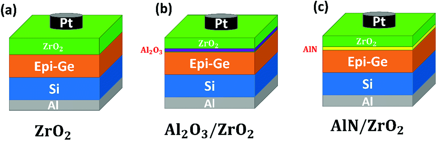 | ||
| Fig. 1 Schematic of the (a) ZrO2, (b) Al2O3/ZrO2, and (c) AlN/ZrO2 gate stacks. | ||
The chemical bonding in the gate stacks was determined by X-ray photoelectron spectroscopy (XPS) using Al Kα radiation at 1486.6 eV. The cross-sectional images of the gate stacks were observed using high-resolution transmission electron microscopy (HRTEM, Philips Tecnai F20 G2 FEI-TEM, 200 kV). The crystalline phases of ZrO2 were measured by grazing incident angle X-ray diffraction (GIXRD) using Cu Kα radiation at an incident angle of 0.5°. The capacitance density versus voltage (C–V), the leakage current density versus voltage (I–V), and the conductance density versus the frequency (G–f) curves of the gate stacks were characterized using an Agilent B1500A semiconductor device analyzer at room temperature.
3. Results and discussions
Fig. 2 shows the Ge 3d XPS spectra of the ZrO2, Al2O3/ZrO2, and AlN/ZrO2 gate stacks with and without the annealing treatment, which reveals the oxidation states of Ge. The XPS spectra can be decomposed into the peaks corresponding to the binding energies at 29.4 eV (Ge), 31.7 eV (GeO), 33.6 eV (GeO2), and 30.9 eV (Ge–N).19 The XPS spectra of the samples without the annealing treatment are shown in Fig. 2(a)–(c). The presence of the GeO oxidation state in the ZrO2 sample (Fig. 2(a)) is attributed to the supply of oxygen from ZrO2. Fig. 2(b) reveals that the interfacial GeO was suppressed in the Al2O3/ZrO2 gate stack compared to that in the ZrO2 sample, which can be deduced from the lower Gibbs free energy of Al2O3 than that of ZrO2.33 It can be seen in Fig. 2(c) that the AlN buffer layer led to the formation of Ge–N bonds, and the GeO oxidation states were almost absent in the AlN/ZrO2 sample because oxygen was not involved during AlN deposition. The result also suggests that the diffusion of oxygen from ZrO2 toward the interface was effectively blocked by the AlN buffer layer, and so the formation of interfacial GeOx was suppressed. Moreover, Fig. 2(d)–(f) are the XPS spectra of the samples treated with the annealing process. As compared with Fig. 2(a) and (b), the annealing treatment gave rise to an increase in the GeO signals and the formation of GeO2 oxidation states in the ZrO2 and Al2O3/ZrO2 gate stacks:34| 2GeO → GeO2 + Ge |
 | ||
| Fig. 2 The Ge 3d XPS spectra of the (a) ZrO2, (b) Al2O3/ZrO2, and (c) AlN/ZrO2 gate stacks without the annealing treatment and the (d) ZrO2, (e) Al2O3/ZrO2, and (f) AlN/ZrO2 gate stacks treated with the annealing process (in a furnace at 450 °C for 30 minutes in N2 ambient). The intensity of the Ge peak of each sample was normalized to one. The annealing treatment facilitated the formation of interfacial GeOx in the ZrO2 and Al2O3/ZrO2 gate stacks. The interfacial GeOx was significantly suppressed in the AlN/ZrO2 gate stack. | ||
The decomposition of GeO into GeO2 and Ge is ascribed to the lower Gibbs free energy of GeO2 than that of GeO.34 The outcome indicates that the annealing process facilitated the formation of interfacial GeOx. Notice that no obvious interfacial GeOx appeared in the XPS spectrum of the AlN/ZrO2 gate stack as shown in Fig. 2(f). The result confirms again that the AlN buffer layer could effectively restrain oxygen diffusion during the ZrO2 deposition and annealing processes.
The Al 2p XPS spectra of the Al2O3/ZrO2 and AlN/ZrO2 gate stacks are shown in Fig. 3. The Al–O bond (75.6 eV) was present in the Al2O3/ZrO2 sample due to the introduction of the Al2O3 buffer layer. The Al 2p peak of the AlN/ZrO2 sample was located near 74.6 eV, which is associated with the Al–N bond because AlN was substituted for the Al2O3 buffer layer.35 Depositing ZrO2 on the AlN buffer layer results in a slight shift in the Al 2p peak (∼75 eV) from the standard Al–N bond at 74.6 eV toward the Al–O bond at 75.6 eV, indicating the partial oxidation of AlN.
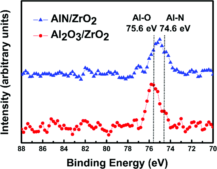 | ||
| Fig. 3 Al 2p XPS spectra of the Al2O3/ZrO2 and AlN/ZrO2 gate stacks. The Al–O (75.6 eV) and Al–N (74.6 eV) bonds were present in the Al2O3/ZrO2 and AlN/ZrO2 samples. | ||
The HRTEM images of the ZrO2, Al2O3/ZrO2, and AlN/ZrO2 gate stacks are shown in Fig. 4. It is seen that the total physical thickness of all the samples was approximately 7.5 nm. The ZrO2 layer featured a crystalline lattice in the images for all of the samples, which demonstrates that ZrO2 was crystallized during thermal annealing.36 In Fig. 4(a), there is an obvious and rough interfacial GeOx layer in the ZrO2 sample. An Al2O3 buffer layer and interfacial GeOx are observed in the Al2O3/ZrO2 gate stack as shown in Fig. 4(b). Fig. 4(c) reveals a sharp interface without interfacial GeOx between AlN and Ge, indicating that the AlN buffer layer was capable of suppressing interfacial GeOx. The HRTEM results are in good agreement with the Ge 3d XPS spectra shown in Fig. 2.
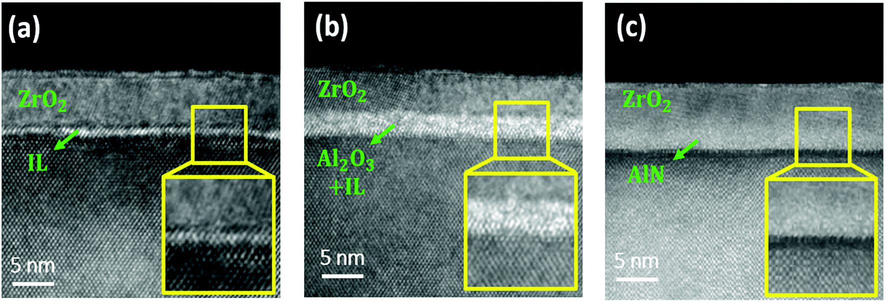 | ||
| Fig. 4 Cross-sectional HRTEM images of the (a) ZrO2, (b) Al2O3/ZrO2, and (c) AlN/ZrO2 gate stacks. There is a sharp interface between AlN and Ge in the AlN/ZrO2 sample. | ||
The GIXRD patterns of the ZrO2, Al2O3/ZrO2, and AlN/ZrO2 gate stacks are shown in Fig. 5. There is an obvious diffraction peak at 2θ = 30.4° in all of the samples, which corresponds to the tetragonal (101) phase (88-1007 JCPDS) or the cubic (111) phase (49-1642 JCPDS) of ZrO2.37 The tetragonal/cubic phase in ZrO2 had a much higher dielectric constant than amorphous ZrO2, which allows further CET scaling.38 Although tetragonal/cubic ZrO2 was thermodynamically stable at temperatures greater than 1170 °C,39,40 the tetragonal/cubic phase had been observed in nanoscale ZrO2 thin films.41 The presence of tetragonal/cubic ZrO2 in the nanoscale layers, as shown in Fig. 5, is consistent with the results of previous studies.36,41
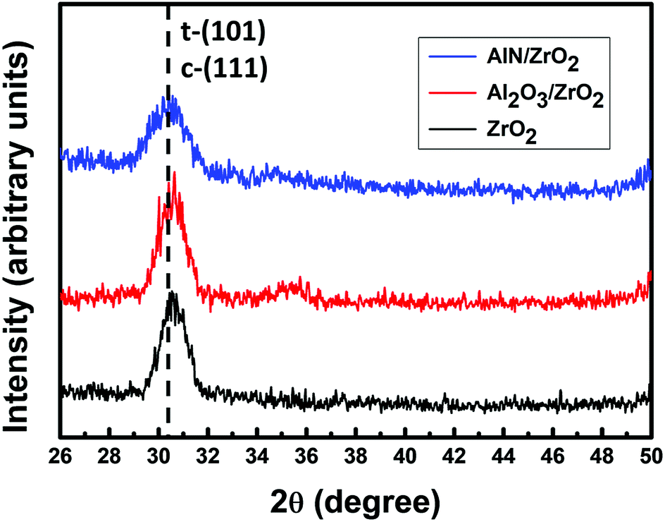 | ||
| Fig. 5 GIXRD patterns of ZrO2, Al2O3/ZrO2, and AlN/ZrO2 gate stacks. The obvious diffraction peak at 2θ = 30.4° is associated with tetragonal/cubic ZrO2. | ||
The C–V curves of the ZrO2, Al2O3/ZrO2, and AlN/ZrO2 gate stacks are shown in Fig. 6(a). The capacitance of the AlN/ZrO2 sample was much greater than that of the ZrO2 and Al2O3/ZrO2 samples. Table 1 shows the CET and the effective dielectric constant (keff) of the ZrO2, Al2O3/ZrO2, and AlN/ZrO2 gate stacks. These values were derived from the C–V curves. The CET and keff values of the ZrO2 sample are 2.35 nm and 12.42 nm, respectively. The keff of the ZrO2 sample is much lower than the dielectric constant of tetragonal/cubic ZrO2,42,43 which can be deduced from the presence of low-K interfacial GeOx in the ZrO2 sample, as shown in the XPS spectrum and the HRTEM image (Fig. 2(d) and 4(a)). Although the low-K interfacial GeOx was suppressed by the Al2O3 buffer layer, as demonstrated by the XPS spectrum (Fig. 2(e)), the introduction of the Al2O3 buffer layer between ZrO2 and Ge still caused a slight degradation of the CET (2.38 nm) and keff (12.29) of the Al2O3/ZrO2 gate stack because Al2O3 has a lower dielectric constant than ZrO2. The substitution of AlN for Al2O3 as the buffer layer led to a significant decrease in the CET (1.75 nm) and an increase in the keff (16.72) of the AlN/ZrO2 sample, which is mainly attributed to the suppression of the interfacial GeOx, as clearly shown in Fig. 2(f) and 4(c).
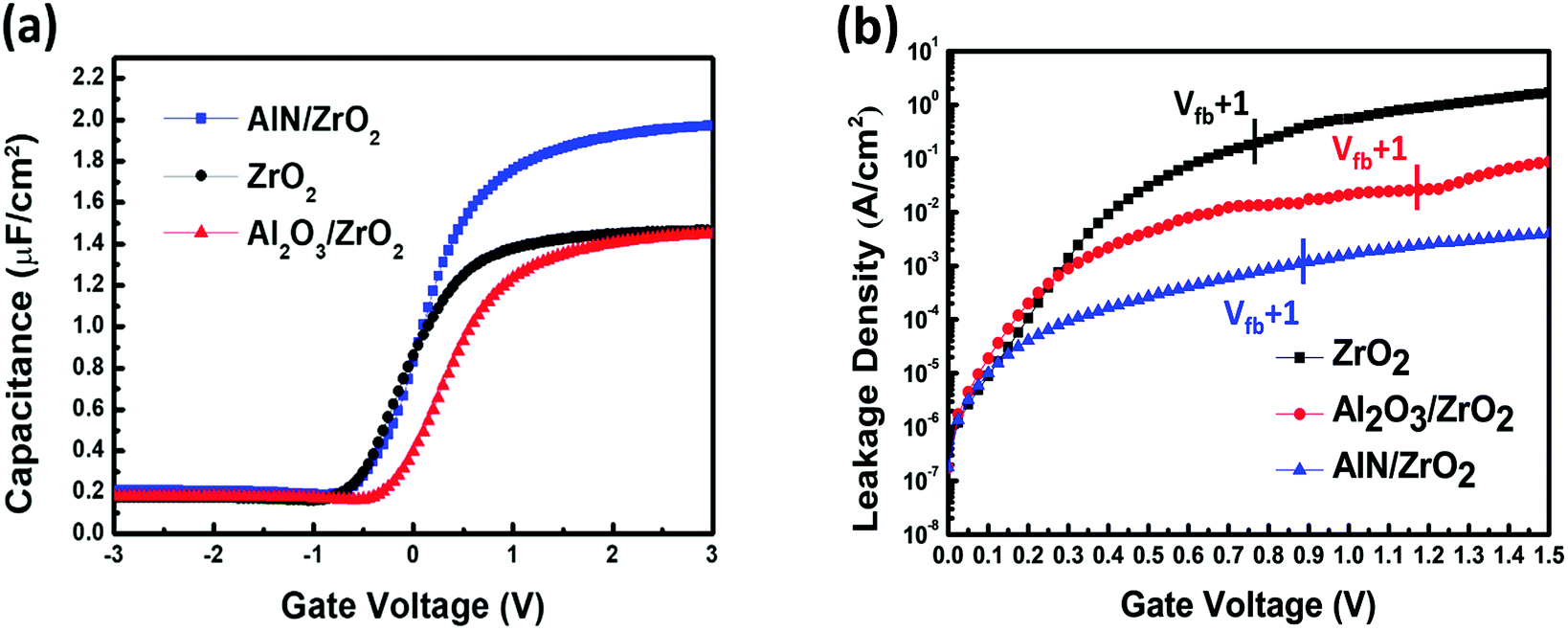 | ||
| Fig. 6 (a) C–V and (b) I–V characteristics of the ZrO2, Al2O3/ZrO2, and AlN/ZrO2 gate stacks. The AlN/ZrO2 gate stack had a higher capacitance and a lower Jg than the ZrO2 or Al2O3/ZrO2 samples. | ||
| Sample | CET (nm) | keff | Jg (A cm−2) | Dit (cm−2 eV−1) |
|---|---|---|---|---|
| a These values were extracted from the C–V, I–V, and G–f curves as shown in Fig. 6 and 7. The leakage current density Jg was determined at Vfb (flat-band voltage) +1 V. The AlN/ZrO2 gate stack exhibited a significant improvement in CET, keff, Jg, and Dit over the ZrO2 and Al2O3/ZrO2 samples. | ||||
| ZrO2 | 2.35 | 12.42 | 1.82 × 10⁻¹ | 9.08 × 10¹² |
| Al2O3/ZrO2 | 2.38 | 12.29 | 2.60 × 10⁻² | 6.46 × 10¹² |
| AlN/ZrO2 | 1.75 | 16.72 | 1.12 × 10⁻³ | 3.85 × 10¹² |
Fig. 6(b) and Table 1 show the I–V curves and the Jg of the ZrO2, Al2O3/ZrO2, and AlN/ZrO2 gate stacks. The ZrO2 sample had a high Jg value of 1.82 × 10⁻¹ A cm−2 as a result of the leakage current path via the grain boundaries in crystalline ZrO2. Due to the high bandgap of Al2O3, the presence of the Al2O3 buffer layer resulted in a decrease in the Jg (2.60 × 10⁻² A cm−2) of the Al2O3/ZrO2 sample. There was a significant reduction in the Jg (1.12 × 10⁻³ A cm−2) of the AlN/ZrO2 gate stack, which is two orders of magnitude lower than that of the ZrO2 sample because of the insertion of the AlN buffer layer. This can be understood from the suppressed growth of interfacial GeOx, which has a low conduction band offset of only ∼0.8 eV.44
The Dit value was measured by the conductance (Nicollian–Goetzberger) method.45,46 Fig. 7(a) shows the equivalent parallel conductance over the angular frequency (GP/ω) as a function of the frequency of the ZrO2, Al2O3/ZrO2, and AlN/ZrO2 gate stacks. The value of Dit was estimated from the maximum value of GP/ω as:45

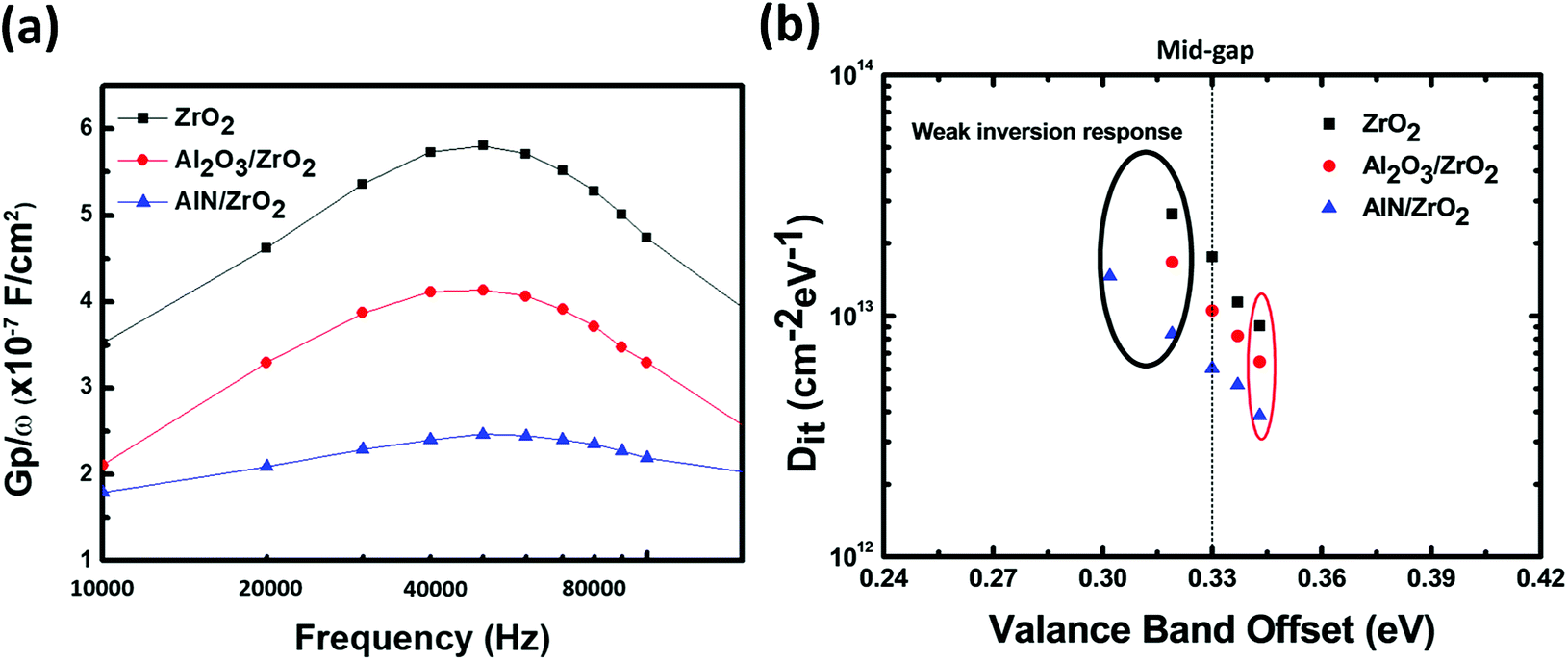 | ||
| Fig. 7 (a) GP/ω versus the frequency of the ZrO2, Al2O3/ZrO2, and AlN/ZrO2 gate stacks. The AlN/ZrO2 gate stack had the lowest value of (GP/ω)max, and so the Dit of the AlN/ZrO2 sample was lower than that of the ZrO2 and Al2O3/ZrO2 gate stacks. (b) Dit distributions versus bandgap energy, which were extracted from the conductance method, of the ZrO2, Al2O3/ZrO2, and AlN/ZrO2 gate stacks. | ||
The C–V curves of the ZrO2, Al2O3/ZrO2, and AlN/ZrO2 gate stacks at various frequencies are shown in Fig. 8. In the frequency range from 1 kHz to 100 kHz, the frequency dispersion is 4.2%, 2.2%, and 1.4% for the ZrO2, Al2O3/ZrO2, and AlN/ZrO2 gate stacks at an accumulation bias of 2 V. The larger capacitance at a high frequency of 1 MHz was deduced from the parasitic inductance.50 The relatively low-frequency dispersion in the AlN/ZrO2 gate stack was correlated with the lower Dit as compared with the ZrO2 and Al2O3/ZrO2 samples.51
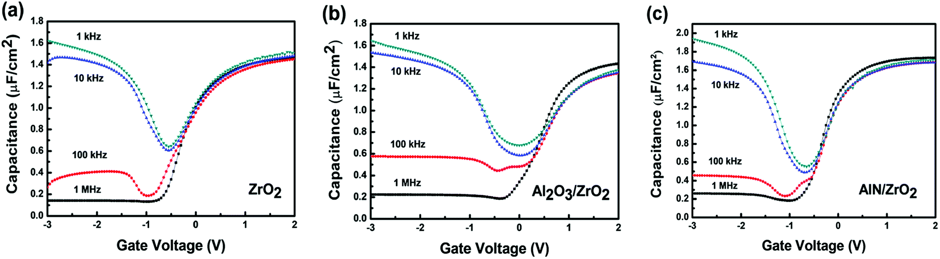 | ||
| Fig. 8 The frequency dependence of the C–V curves of the (a) ZrO2, (b) Al2O3/ZrO2, and (c) AlN/ZrO2 gate stacks. Low-frequency dispersion was observed in the AlN/ZrO2 sample. | ||
4. Conclusion
In this study, the electrical and structural characteristics of the ZrO2, Al2O3/ZrO2, and AlN/ZrO2 gate stacks on Ge were investigated carefully. The introduction of an Al2O3 buffer layer between ZrO2 and Ge resulted in a decrease of Jg value due to the high bandgap of Al2O3. However, it is difficult to prevent the growth of unstable, low-K interfacial GeOx using an Al2O3 buffer layer because oxygen was involved during the deposition of Al2O3. The formation of interfacial GeOx was significantly suppressed by an AlN buffer layer, as evidenced by the XPS and HRTEM characterizations. This produced a significant enhancement in the electrical characteristics, including the CET, keff, Jg, and Dit of the AlN/ZrO2 gate stack. The results of this study show that an AlN buffer layer is an effective approach to high-quality interfacial engineering for high-performance high-K gate stacks in advanced Ge MOS transistors.Conflicts of interest
There are no conflicts to declare.Acknowledgements
The authors gratefully acknowledge the financial support of the Taiwan Semiconductor Manufacturing Company (TSMC) and the Ministry of Science and Technology (MOST 107-2622-8-002-018), Taiwan.References
- S. Takagi, et al., IEDM'03 Technical Digest, IEEE International, 2003, pp. 3.3.1–3.3.4 Search PubMed.
- M. V. Fischetti and S. E. Laux, J. Appl. Phys., 1996, 80(4), 2234–2252 CrossRef CAS.
- K. Saraswat, C. O. Chui, T. Krishnamohan, D. Kim, A. Nayfeh and A. Pethe, Mater. Sci. Eng., B, 2006, 135(3), 242–249 CrossRef CAS.
- S. Takagi, M. Noguchi, M. Kim, S.-H. Kim, C.-Y. Chang and M. Yokoyama, et al., Solid-State Electron., 2016, 125, 82–102 CrossRef CAS.
- K. Prabhakaran, F. Maeda, Y. Watanabe and T. Ogino, Appl. Phys. Lett., 2000, 76(16), 2244–2246 CrossRef CAS.
- Y. Seo, T. I. Lee, C. M. Yoon, B.-E. Park, W. S. Hwang and H. Kim, et al., IEEE Trans. Electron Devices, 2017, 64(8), 3303–3307 CAS.
- G. He, X. Chen and Z. Sun, Surf. Sci. Rep., 2013, 68(1), 68–107 CrossRef CAS.
- G. He, J. Gao, H. Chen, J. Cui, Z. Sun and X. Chen, ACS Appl. Mater. Interfaces, 2014, 6(24), 22013–22025 CrossRef CAS PubMed.
- G. He, B. Deng, H. Chen, X. Chen, J. Lv and Y. Ma, et al., APL Mater., 2013, 1(1), 012104 CrossRef.
- G. He, J. Liu, H. Chen, Y. Liu, Z. Sun and X. Chen, et al., J. Mater. Chem. C, 2014, 2(27), 5299–5308 RSC.
- Q. Xie, S. Deng, M. Schaekers, D. Lin, M. Caymax and A. Delabie, et al., Semicond. Sci. Technol., 2012, 27(7), 074012 CrossRef.
- J. Zhang, G. He, L. Zhou, H. Chen, X. Chen and X. Chen, et al., J. Alloys Compd., 2014, 611, 253–259 CrossRef CAS.
- V. Afanas'ev and A. Stesmans, Appl. Phys. Lett., 2004, 84(13), 2319–2321 CrossRef.
- Y. Fukuda, K. Kato, H. Toyota, T. Ono, Y. Nagasato and T. Ueno, Jpn. J. Appl. Phys., 2006, 45(9S), 7351 CrossRef CAS.
- R. Zhang, T. Iwasaki, N. Taoka, M. Takenaka and S. Takagi, Appl. Phys. Lett., 2011, 98(11), 112902 CrossRef.
- P. Zimmerman, et al., IEDM'06, IEEE International, 2006, pp. 1–4 Search PubMed.
- C.-C. Lin, Y.-H. Wu, C.-Y. Wu and C.-W. Lee, IEEE Electron Device Lett., 2014, 35(3), 384–386 CAS.
- S. Iwauchi and T. Tanaka, Jpn. J. Appl. Phys., 1971, 10(2), 260 CrossRef CAS.
- R. Zhang, T. Iwasaki, N. Taoka, M. Takenaka and S. Takagi, IEEE Trans. Electron Devices, 2012, 59(2), 335–341 CAS.
- C. O. Chui, F. Ito and K. C. Saraswat, IEEE Electron Device Lett., 2004, 25(9), 613–615 CrossRef CAS.
- C. O. Chui, F. Ito and K. C. Saraswat, IEEE Trans. Electron Devices, 2006, 53(7), 1501–1508 CAS.
- T. Maeda, T. Yasuda, M. Nishizawa, N. Miyata, Y. Morita and S. Takagi, Appl. Phys. Lett., 2004, 85(15), 3181–3183 CrossRef CAS.
- T. Maeda, M. Nishizawa, Y. Morita and S. Takagi, Appl. Phys. Lett., 2007, 90(7), 072911 CrossRef.
- Y. Otani, Y. Itayama, T. Tanaka, Y. Fukuda, H. Toyota and T. Ono, et al., Appl. Phys. Lett., 2007, 90(14), 142114 CrossRef.
- G. V. Rao, M. Kumar, T. Rajesh, D. R. K. Reddy, D. Anjaneyulu and B. Sainath, et al., Materials Today: Proceedings, 2018, 5(1), 650–656 CrossRef.
- Y. J. Lee, J. Cryst. Growth, 2004, 266(4), 568–572 CrossRef CAS.
- A. Ahmed, A. Rys, N. Singh, J. Edgar and Z. Yu, J. Electrochem. Soc., 1992, 139(4), 1146–1151 CrossRef CAS.
- M. Morita, S. Isogai, K. Tsubouchi and N. Mikoshiba, Appl. Phys. Lett., 1981, 38(1), 50–52 CrossRef CAS.
- X.-H. Xu, H.-S. Wu, C.-J. Zhang and Z.-H. Jin, Thin Solid Films, 2001, 388(1–2), 62–67 CrossRef CAS.
- A. C. Jones, C. R. Whitehouse and J. S. Roberts, Chem. Vap. Deposition, 1995, 1(3), 65–74 CrossRef CAS.
- D. Riihelä, M. Ritala, R. Matero, M. Leskelä, J. Jokinen and P. Haussalo, Chem. Vap. Deposition, 1996, 2(6), 277–283 CrossRef.
- P. Kelly and R. Arnell, Vacuum, 2000, 56(3), 159–172 CrossRef CAS.
- G. Thompson, P. Skeldon, X. Zhou, K. Shimizu, H. Habazaki and C. Smith, Aircr. Eng., 2003, 75(4), 372–379 CrossRef.
- S. Kai Wang, H.-G. Liu and A. Toriumi, Appl. Phys. Lett., 2012, 101(6), 061907 CrossRef.
- P. Motamedi and K. Cadien, Appl. Surf. Sci., 2014, 315, 104–109 CrossRef CAS.
- J.-J. Huang, L.-T. Huang, M.-C. Tsai, M.-H. Lee and M.-J. Chen, Appl. Surf. Sci., 2014, 305, 214–220 CrossRef CAS.
- C. Zhao, S. Taylor, M. Werner, P. Chalker, R. Murray and J. Gaskell, et al., J. Appl. Phys., 2009, 105(4), 044102 CrossRef.
- D. Vanderbilt, X. Zhao and D. Ceresoli, Thin Solid Films, 2005, 486(1–2), 125–128 CrossRef CAS.
- J. Robertson, Rep. Prog. Phys., 2005, 69(2), 327 CrossRef.
- S. Bang, S. Lee, S. Jeon, S. Kwon, W. Jeong and S. Kim, et al., J. Electrochem. Soc., 2008, 155(9), H633–H637 CrossRef CAS.
- C. Scanlan, M. Gajdardziska-Josifovska and C. Aita, Appl. Phys. Lett., 1994, 64(26), 3548–3550 CrossRef CAS.
- Y.-H. Wu, L.-L. Chen, R.-J. Lyu, M.-Y. Li and H.-C. Wu, IEEE Electron Device Lett., 2010, 31(9), 1014–1016 CAS.
- R. Hegde, D. Triyoso, S. Samavedam and B. White Jr, J. Appl. Phys., 2007, 101(7), 074113 CrossRef.
- J. Robertson and R. M. Wallace, Mater. Sci. Eng., R, 2015, 88, 1–41 CrossRef.
- R. Engel-Herbert, Y. Hwang and S. Stemmer, J. Appl. Phys., 2010, 108(12), 124101 CrossRef.
- E. H. Nicollian, J. R. Brews and E. H. Nicollian, MOS (metal oxide semiconductor) physics and technology, Wiley, New York, 1982 Search PubMed.
- K. Martens, C. O. Chui, G. Brammertz, B. De Jaeger, D. Kuzum and M. Meuris, et al., IEEE Trans. Electron Devices, 2008, 55(2), 547 CAS.
- C.-C. Hsu, W.-C. Chi, Y.-H. Tsai, M.-L. Tsai, S.-Y. Wang and C.-H. Chou, et al., J. Vac. Sci. Technol., B, 2018, 36(5), 051204 CrossRef.
- A. Nayfeh, C. O. Chui, K. C. Saraswat and T. Yonehara, Appl. Phys. Lett., 2004, 85(14), 2815–2817 CrossRef CAS.
- C.-M. Lin, H.-C. Chang, I.-H. Wong, S.-J. Luo, C. Liu and C. Hu, Appl. Phys. Lett., 2013, 102(23), 232906 CrossRef.
- F. Ji, J. Xu, P. Lai, C. Li and J. Liu, IEEE Electron Device Lett., 2011, 32(2), 122–124 CAS.
| This journal is © The Royal Society of Chemistry 2019 |