
Design and performance study of high efficiency/low efficiency roll-off/high CRI hybrid WOLEDs based on aggregation-induced emission materials as fluorescent emitters†
Zeng
Xu
 a,
Jiabao
Gu
a,
Jian
Huang
a,
Chengwei
Lin
a,
Yuanzhao
Li
a,
Dezhi
Yang
a,
Xianfeng
Qiao
a,
Anjun
Qin
a,
Zujin
Zhao
a,
Ben Zhong
Tang
*ab and
Dongge
Ma
*a
a,
Jiabao
Gu
a,
Jian
Huang
a,
Chengwei
Lin
a,
Yuanzhao
Li
a,
Dezhi
Yang
a,
Xianfeng
Qiao
a,
Anjun
Qin
a,
Zujin
Zhao
a,
Ben Zhong
Tang
*ab and
Dongge
Ma
*a
aCenter for Aggregation-Induced Emission, Institute of Polymer Optoelectronic Materials and Devices, State Key Laboratory of Luminescent Materials and Devices, South China University of Technology, Guangzhou, 510640, China. E-mail: msdgma@scut.edu.cn
bDepartment of Chemistry, Hong Kong Branch of Chinese National Engineering Research Center for Tissue Restoration and Reconstruction, The Hong Kong University of Science & Technology, Clear Water Bay, Kowloon, Hong Kong, China. E-mail: tangbenz@ust.hk
First published on 1st October 2019
Abstract
Generally, hybrid white organic light-emitting diodes (WOLEDs) are constructed with blue fluorophores and yellow or green/red phosphors, and the fluorophores and phosphors used have to be doped into proper hosts to avoid the exciton quenching caused by molecular aggregation, which brings difficulties in device structure design and fabrication. In this paper, we fabricated high efficiency/low efficiency roll-off/high CRI hybrid WOLEDs based on aggregation-induced emission (AIE) luminogens (AIEgens) with non-doping features as the fluorophore emitters. The resulting WOLEDs were constructed by two AIEgens that emit blue and green light, respectively, and a doped red phosphor, greatly simplifying the device structure. Encouragingly, the hybrid WOLEDs simultaneously achieved high efficiency (PEmax = 50.5 lm W−1, EQEmax = 20.5%), low efficiency roll-off (PE1000nit = 32.9 lm W−1, EQE1000nit = 18.9%), and high CRI (≥90). Our results indicate that AIEgens are promising material systems for manufacturing high-performance white OLEDs with a simple device structure.
1. Introduction
With increasingly serious eye injuries from conventional lighting devices, the development of healthy light sources has become urgent.1–3 White organic light-emitting diodes (WOLEDs) are known to have the merits of surface emission, low blue, soft light, high color rendering index (CRI), being sun-like light, and no dazzle, and are thus regarded as the ideal lighting sources for humanity.4–8 Currently, high efficiency and low efficiency roll-off are the basic requirements for the application of WOLEDs, and a large amount of research is focused on these two aspects. However, the conventional materials exhibit aggregation-caused quenching (ACQ) characteristics, which leads to inevitable exciton quenching in non-doped cases. To alleviate the ACQ phenomenon, doping techniques have been largely adopted in the fabrication of OLEDs.5–7,9–11 The situation in WOLEDs is more complicated, where multi-source doping and complicated emitting layer structures are widely employed to ensure the full utilization of excitons for radiative decay and stable spectral emission.12–14 This greatly increases the difficulty of the process, resulting in an increase in cost.Aggregation-induced emission (AIE) luminogens (AIEgens) exhibit superior solid emission that can efficiently close the exciton quenching channels in non-doped film states.15–18 Some recent reports have demonstrated that OLEDs based on non-doped AIEgens exhibit the properties of high efficiency and low roll-off.19–24 In order to further improve the efficiency of OLEDs based on AIEgens, some new AIE materials have been synthesized by combining the concepts of thermal active delayed fluorescence (TADF), hybrid local charge transfer (HLCT), and triplet–triplet annihilation (TTA) that utilizes triplets to achieve high efficiency fluorescence emission.21,25–27 For example, the aggregation-induced delayed fluorescence (AIDF) materials, which were first developed by Yasuda, exhibited high efficiency and low roll-off in non-doped OLEDs.28 Later a series of green and yellow AIDF materials that realize high external quantum efficiencies (EQEs) above 20% with very low roll-off of about 10% at a luminance of 5000 cd m−2 were reported in non-doped OLEDs.29,30
In this work, we used non-doped AIEgens as the blue and green emitting layers and a red phosphor doped TCTA host as the red emitting layer to construct three-color hybrid WOLEDs. Impressively, the fabricated WOLEDs simultaneously achieved a high power efficiency (PE) and EQE of 50.5 lm W−1 and 20.5%, a low efficiency roll-off with PE1000nit and EQE1000nit of 32.9 lm W−1 and 18.9%, and a high CRI above 90. Furthermore, the color correlated temperature (CCT) can be easily adjusted through simply changing the EML thickness to meet the needs of different lighting applications.
2. Results and discussion
As shown in Fig. 1a–c, we selected a blue AIEgen, namely 4′-(4-(diphenylamino)phenyl)-5′-phenyl-[1,1′:2′,1′′-terphenyl]-4-carbonitrile (TPB-AC), to act as the blue emitting layer. It has been shown that TPB-AC possesses a high PL quantum yield (ΦPL) of 98.6% and a high horizontal dipole ratio (Θ‖) of 79%, and blue OLEDs based on TPB-AC achieved an EQE as high as 7.0%.31,32 Moreover, we chose a green AIDF material, namely (4-(10H-phenoxazin-10-yl)phenyl)(9-phenyl-9H-carbazol-3-yl)methanone (CP-BP-PXZ), as the green emitting layer. As shown, CP-BP-PXZ has a high ΦPL of 58% and the EQE of the fabricated non-doped OLEDs reached 18.2% with an extremely low efficiency roll-off of 1.2% at a luminance of 1000 cd m−2.29 Furthermore, CP-BP-PXZ also emits a broad spectrum with a FWHM (full width at half maxima) of 103 nm (as shown in Fig. S1, ESI†), which is very important for WOLEDs to improve their spectral coverage. In our WOLEDs, the red emitting layer was formed by doping red phosphor Ir(dmppr-mp)2(divm) in 4,4′,4′′-tri(N-carbazolyl)triphenylamine (TCTA) as the host. Based on these three emitting layers, two kinds of structure schemes were promoted, as shown in Fig. 1a and b. In these two devices, indium tin oxide (ITO) acts as the anode, 1,4,5,8,9,11-hexaazatriphenylene hexacarbonitrile (HAT-CN) and LiF are chosen to act as the hole- and electron-injecting layers, respectively, 1-bis[4-[N,N-di(4-tolyl)amino]phenyl]-cyclo-hexane (TAPC) and 4,4′,4′′-tri(N-carbazolyl)triphenylamine (TCTA) are used as the hole transporting and electron/exciton-blocking layers (HTL/EBL), 1,3,5-tri(m-pyrid-3-yl-phenyl)benzene (TmPyPB) is employed for the electron-transporting layer (ETL), and Al is selected as the cathode.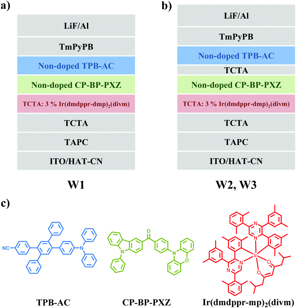 | ||
| Fig. 1 (a) Structure diagram of the designed device W1 without an interlayer. (b) Structure diagram of the designed device W2 with a TCTA interlayer. (c) Chemical structures of TPB-AC, CP-BP-PXZ, and Ir(dmppr-mp)2(divm). | ||
Fig. 1a shows the configuration of device W1 without a TCTA interlayer between TPB-AC and CP-BP-PXZ, which is ITO/HAT-CN (5 nm)/TAPC (50 nm)/TCTA (5 nm)/TCTA: 3 wt% Ir(dmppr-mp)2(divm) (8 nm)/CP-BP-PXZ (8 nm)/TPB-AC (10 nm)/TmPyPB (40 nm)/LiF (1 nm)/Al (120 nm). As shown in Fig. 2c, Table 1 and Fig. S2 (ESI†), device W1 exhibits maximum forward-viewing CE (current efficiency), PE (power efficiency), and EQE (external quantum efficiency) of 19.8 cd A−1, 19.7 lm W−1, and 12.0%, respectively. At a luminance of 1000 cd m−2, the efficiencies remain at 19.8 cd A−1, 17.7 lm W−1, and 11.5%, respectively. The efficiency roll-offs of PE and EQE achieve small values of 10.2% and 4.2%, respectively. Moreover, device W1 realizes a high color rendering index (CRI) of 87 at a luminance of 1000 cd m−2 with Commission Internationale de I’Eclairage (CIE) coordinates of (0.54, 0.44), indicating the validity of AIEgens as emitters in the fabrication of high efficiency and low efficiency roll-off hybrid WOLEDs. To further enhance the efficiencies, we fabricated device W2 by inserting a TCTA interlayer between TPB-AC and CP-BP-PXZ. The detailed configuration is ITO/HAT-CN (5 nm)/TAPC (50 nm)/TCTA (5 nm)/TCTA: 3 wt% Ir(dmppr-mp)2(divm) (8 nm)/CP-BP-PXZ (7 nm)/TCTA (2 nm)/TPB-AC (10 nm)/TmPyPB (40 nm)/LiF (1 nm)/Al (120 nm). As shown in Fig. 2d–f, device W2 exhibits better EL performance than device W1. The turn-on voltage is 2.4 V (Fig. 2e) and the maximum forward-viewing CE, PE and EQE are 40.6 cd m−2, 50.5 lm W−1, and 20.5%, respectively (Fig. 2f, Table 1 and Fig. S3 (ESI†)). Furthermore, at a luminance of 1000 cd m−2, the efficiencies remain at 38.7 cd m−2, 32.9 lm W−1, and 18.9%, respectively, with relatively low CE, PE, and EQE roll-offs of 4.7, 34.9, and 7.8%, respectively. Especially, the spectrum is very stable and shows a small CIE coordinate variation of (0.02, 0.02) from a luminance of 1000 cd m−2 (0.52, 0.45) to 10![[thin space (1/6-em)]](https://www.rsc.org/images/entities/char_2009.gif) 000 cd m−2 (0.50, 0.43). Importantly, the color rendering index (CRI) of device W2 reaches 90 at a luminance of 1000 cd m−2, which is an excellent performance for healthy lighting. Obviously, the TCTA interlayer plays a very important role in improving the EL performance of device W2. Moreover, we realized color-tunable hybrid WOLEDs (device W3) by changing the thicknesses of the emitting layers and the interlayer. The configuration of device W3 is ITO/HAT-CN (5 nm)/TAPC (50 nm)/TCTA (5 nm)/TCTA: 3 wt% Ir(dmppr-mp)2(divm) (5 nm)/CP-BP-PXZ (10 nm)/TCTA (3 nm)/TPB-AC (10 nm)/TmPyPB (40 nm)/LiF (1 nm)/Al (120 nm). As shown in Fig. 2i, Table 1 and Fig. S4 (ESI†), device W3 shows maximum forward-viewing CE, PE, and EQE of 42.1 cd A−1, 51.0 lm W−1, and 17.8%, respectively, and they remain at 38.8 cd A−1, 31.0 lm W−1, and 16.4% at a luminance of 1000 cd m−2, respectively. Different from device W2, device W3 exhibits changeable CIE coordinate spectra from (0.46, 0.49) at 1076 cd m−2 to (0.35, 0.33) at 24625 cd m−2. The maximum CRI reaches 97 at a luminance of 7810 cd m−2 and CIE coordinates of (0.41, 0.42), and can also reach 91 at the pure white emission with CIE coordinates of (0.35, 0.33). This is a very useful feature in practical lighting applications.
000 cd m−2 (0.50, 0.43). Importantly, the color rendering index (CRI) of device W2 reaches 90 at a luminance of 1000 cd m−2, which is an excellent performance for healthy lighting. Obviously, the TCTA interlayer plays a very important role in improving the EL performance of device W2. Moreover, we realized color-tunable hybrid WOLEDs (device W3) by changing the thicknesses of the emitting layers and the interlayer. The configuration of device W3 is ITO/HAT-CN (5 nm)/TAPC (50 nm)/TCTA (5 nm)/TCTA: 3 wt% Ir(dmppr-mp)2(divm) (5 nm)/CP-BP-PXZ (10 nm)/TCTA (3 nm)/TPB-AC (10 nm)/TmPyPB (40 nm)/LiF (1 nm)/Al (120 nm). As shown in Fig. 2i, Table 1 and Fig. S4 (ESI†), device W3 shows maximum forward-viewing CE, PE, and EQE of 42.1 cd A−1, 51.0 lm W−1, and 17.8%, respectively, and they remain at 38.8 cd A−1, 31.0 lm W−1, and 16.4% at a luminance of 1000 cd m−2, respectively. Different from device W2, device W3 exhibits changeable CIE coordinate spectra from (0.46, 0.49) at 1076 cd m−2 to (0.35, 0.33) at 24625 cd m−2. The maximum CRI reaches 97 at a luminance of 7810 cd m−2 and CIE coordinates of (0.41, 0.42), and can also reach 91 at the pure white emission with CIE coordinates of (0.35, 0.33). This is a very useful feature in practical lighting applications.
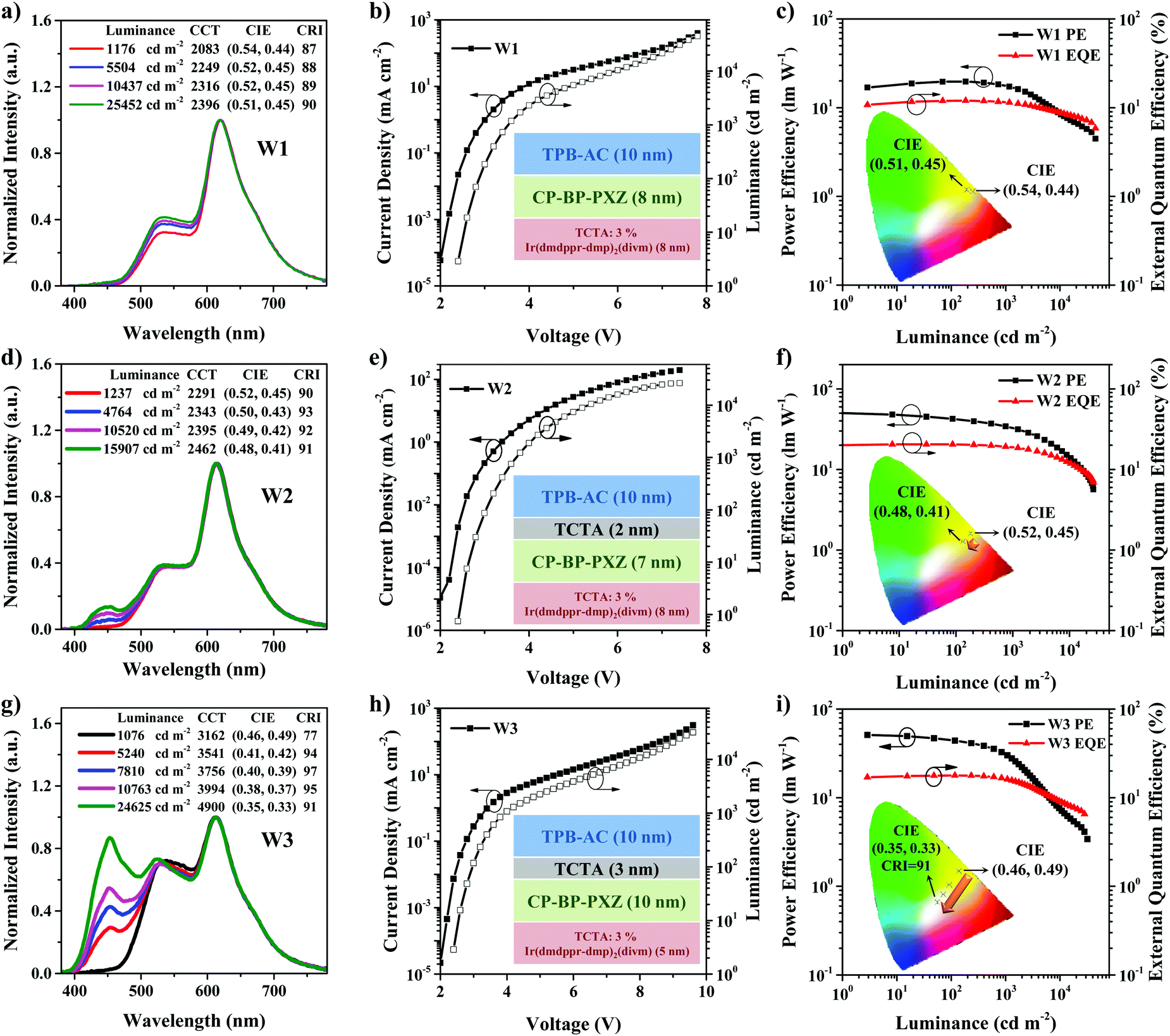 | ||
| Fig. 2 (a) Normalized EL spectra of device W1 at different luminances. (b) Current density–luminance–voltage characteristics of device W1. Inset: The structure of the emitting layers in device W1. (c) Power efficiency and external quantum efficiency as a function of luminance for device W1. Inset: Diagram of the CIE coordinates for device W1. (d) Normalized EL spectra of device W2 at different luminances. (e) Current density–luminance–voltage characteristics of device W2. Inset: The structure of the emitting layer in device W2. (f) Power efficiency and external quantum efficiency as a function of luminance for device W2. Inset: Diagram of the CIE coordinates for device W2. (g) Normalized EL spectra of device W3 at different luminances. (h) Current density–luminance–voltage characteristics of device W3. Inset: The structure of the emitting layer in device W3. (i) Power efficiency and external quantum efficiency as a function of luminance for device W3. Inset: Diagram of the CIE coordinates for device W3. | ||
| Device | V on (V) | L max (cd m−2) | CEc (cd A−1) | PEc (lm W−1) | EQEc (%) | CRId | CIEe (x, y) |
|---|---|---|---|---|---|---|---|
| a V on is the turn-on voltage, which is measured at 1 cd m−2. b L max is the maximum luminance. c Order of measured value: maximum, then values at 1000 cd m−2. d Color rendering index (CRI) is measured at 1000 cd m−2, then the maximum. e Commission Internationale de I’Eclairage (CIE) coordinates are measured at 1000 cd m−2. | |||||||
| W1 | 2.4 | 44797 |
19.8/19.8 | 19.7/17.7 | 12.0/11.5 | 87, 89 | (0.54, 0.44) |
| W2 | 2.4 | 26486 |
40.6/38.7 | 50.5/32.9 | 20.5/18.9 | 90, 93 | (0.52, 0.45) |
| W3 | 2.6 | 33983 |
42.1/38.8 | 51.0/31.0 | 17.8/16.4 | 77, 97 | (0.49, 0.46) |
To gain insight into the mechanisms of devices W1, W2, and W3, we first analyzed the energy levels of the singlet and triplet states of CP-BP-PXZ and TPB-AC. As shown in Fig. 3a and b, TPB-AC has a high S1 of 2.77 eV and a relatively low T1 of 2.48 eV. However, CP-BP-PXZ shows a small ΔEST owing to its AIDF characteristic, which causes a S1 of 2.34 eV and a high T1 of 2.32 eV. As we can see, the small energy gap of 0.16 eV between T1,G and T1,B may cause a DET process from T1,G to T1,B, leading to the exciton quenching. This should be the major reason for device W1 showing low efficiency. As is known, FRET processes have a radius of about 10 nm while DET processes are less than 3 nm. Thus, the FRET process is rarely influenced if we introduce a thin interlayer to block the DET process. Therefore, in devices W2 and W3, the introduction of the TCTA interlayer largely decreases the unfavorable DET processes between CP-BP-PXZ and TPB-AC, thus eliminating the non-radiative channels. Moreover, the TCTA interlayer also plays a regulative function of exciton distribution. As shown in Fig. 3c and d, the thicker TCTA interlayer efficiently blocks electrons and excitons in the TPB-AC blue layer, resulting in more blue emission for device W3 than device W2 (Fig. 2d and g).
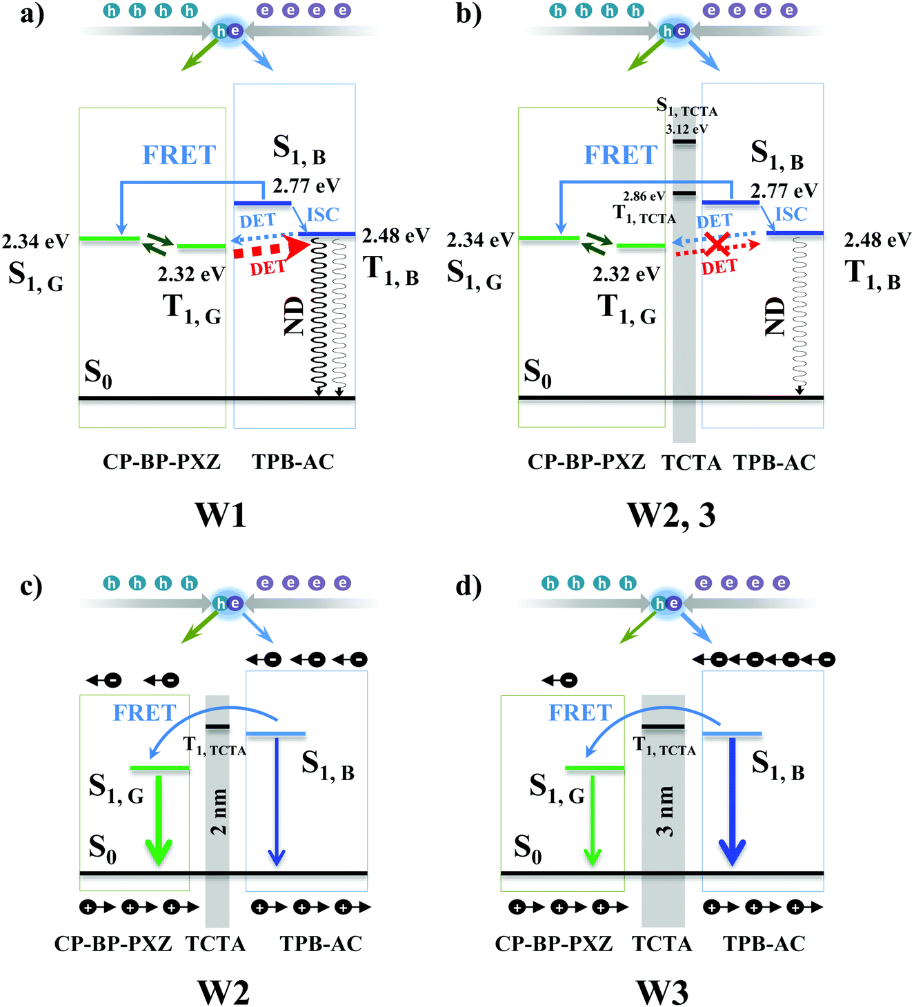 | ||
| Fig. 3 Energy levels and energy transfer processes in the CP-BP-PXZ and TPB-AC layers in devices W1 (a) and W2 (or W3) (b). Schematic diagrams of the exciton emission in the CP-BP-PXZ and TPB-AC layers in devices W2 (c) and W3 (d). Here, S1,B, S1,G and S1,TCTA are the singlet energy levels of TPB-AC, CP-BP-PXZ, and TCTA, respectively. T1,B, T1,G and T1,TCTA are the triplet energy levels of TPB-AC, CP-BP-PXZ, and TCTA, respectively. FRET and DET are the Förster energy transfer and the Dexter energy transfer, respectively. ND is the non-radiative decay. | ||
Furthermore, we measured the absorption spectra of the Ir(dmppr-mp)2(divm) and CP-BP-PXZ films and the PL spectra of the CP-BP-PXZ and TPB-AC films. As shown in Fig. 4b, there is a large overlap between the absorption spectra of Ir(dmppr-mp)2(divm) and the PL spectra of CP-BP-PXZ and TPB-AC, and between CP-BP-PXZ and TPB-AC, indicating the efficient energy transfer from CP-BP-PXZ and TPB-AC to Ir(dmppr-mp)2(divm) and from TBP-AC to CP-BP-PXZ. Then, we manufactured four films to further investigate the energy transfer processes. The structures of films 1–4 are shown in Fig. 4a, and the PL of films 1–4 are shown in Fig. S6 (ESI†). As shown in Fig. 4c, the CP-BP-PXZ emission in film 1 exhibits a promoted lifetime of 24.6 ns and a delayed lifetime of 1641 ns. However, after adding an Ir(dmppr-mp)2(divm) doped layer adjacent to the CP-BP-PXZ (film 2), the lifetimes of the CP-BP-PXZ emission in film 2 are reduced to 21.9 ns and 1331 ns, respectively. It is obvious that the emissions of the promoted and delayed fluorescence from CP-BP-PXZ are quenched by Ir(dmppr-mp)2(divm), indicating the efficient Förster (FRET) and Dexter (DET) energy transfer processes from CP-BP-PXZ to Ir(dmppr-mp)2(divm). As shown in Fig. 4d, the TPB-AC emission in film 3 exhibits a lifetime of 1.62 ns. However, after evaporating an additional CP-BP-PXZ layer to fabricate film 4 with CP-BP-PXZ/TCTA/TPB-AC, the lifetime of the TPB-AC emission is reduced to 0.78 ns. This means that an efficient energy transfer from TPB-AC to CP-BP-PXZ occurs, and the FRET process is mainly due to the existence of the 2 nm thick TCTA interlayer.
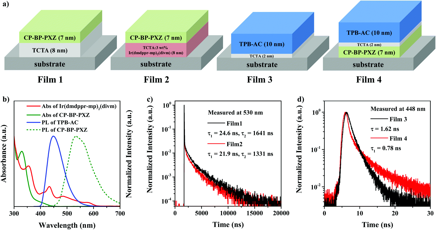 | ||
| Fig. 4 (a) Structures of films 1–4. (b) Absorption spectra of the Ir(dmppr-mp)2(divm) and CP-BP-PXZ films, and PL spectra of the CP-BP-PXZ and TPB-AC films. (c) Transient PL spectra of films 1 and 2 measured at 530 nm. (d) Transient PL spectra of films 3 and 4 measured at 448 nm. | ||
To gain insight into the charge carrier trapping processes in white OLEDs, we fabricated hole-only devices with the configuration ITO/HAT-CN (5 nm)/TAPC (50 nm)/TCTA (5 nm)/TCTA: x wt% Ir(dmppr-mp)2(divm) (20 nm)/TCTA (5 nm)/TAPC (50 nm)/HAT-CN (5 nm)/Al (120 nm), and electron-only devices with the configuration ITO/LiF (1 nm)/TmPyPB (40 nm)/TCTA: x wt% Ir(dmppr-mp)2(divm) (20 nm)/TmPyPB (40 nm)/LiF (1 nm)/Al (120 nm). Here, x = 0 for devices H1 and E1, x = 1 for devices H2 and E2, x = 2 for devices H3 and E3, and x = 3 for devices H4 and E4. As shown in Fig. 5a and b, with the increase of the red phosphor doping concentration, the electron and hole currents are obviously reduced, indicating the significant trapping effects of Ir(dmppr-mp)2(divm) on holes and electrons. Moreover, we manufactured devices C1–C3 with the configuration of ITO/HAT-CN (5 nm)/TAPC (50 nm)/TCTA (5 nm)/TCTA: y wt% Ir(dmppr-mp)2(divm) (8 nm)/CP-BP-PXZ (7 nm)/TCTA (2 nm)/TPB-AC (10 nm)/TmPyPB (40 nm)/LiF (1 nm)/Al (120 nm), similar to the structure of white device W2, where y = 0 for device C1, y = 1 for device C2, and y = 2 for device C3. The EL spectra of devices C1–C3, and W2 are shown in Fig. S5 (ESI†). As we can see, the red emission grows with increasing Ir(dmppr-mp)2(divm) doping concentration. Then, we also measured the capacitance–voltage characteristics of devices C1, C2, C3, and W2. As shown in Fig. 5c, the capacitance of the devices raises when increasing the doping concentration of Ir(dmppr-mp)2(divm) in TCTA. These results further prove that the emission of red phosphor in white devices W2 and W3 also includes charge carrier trapping processes.
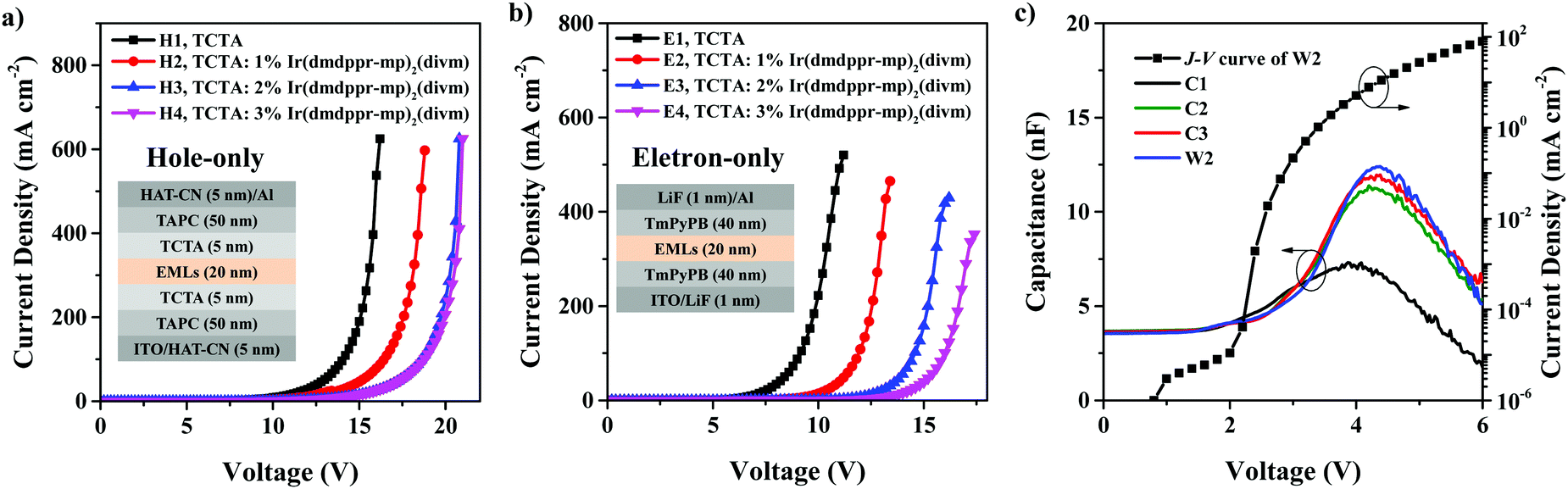 | ||
| Fig. 5 (a) Current density–voltage characteristics of the hole-only devices H1–H4. Inset: Devices H1–H4 with the configuration of ITO/HAT-CN (5 nm)/TAPC (50 nm)/TCTA (5 nm)/TCTA: x wt% Ir(dmppr-mp)2(divm) (20 nm)/TCTA (5 nm)/TAPC (50 nm)/HAT-CN (5 nm)/Al (120 nm). (b) Current density–voltage characteristics of the electron-only devices E1–E4. Inset: Devices E1–E4 with the configuration of ITO/LiF (1 nm)/TmPyPB (40 nm)/TCTA: x wt% Ir(dmppr-mp)2(divm) (20 nm)/TmPyPB (40 nm)/LiF (1 nm)/Al (120 nm), where x = 0 for devices H1 and E1, x = 1 for H2 and E2, x = 2 for H3 and E3, and x = 3 for H4 and E4. (c) Capacitance–voltage characteristics of devices C1–C3, and W2 and current density–voltage characteristic of device W2. Device structure: ITO/HAT-CN (5 nm)/TAPC (50 nm)/TCTA (5 nm)/TCTA: y wt% Ir(dmppr-mp)2(divm) (8 nm)/CP-BP-PXZ (7 nm)/TCTA (2 nm)/TPB-AC (10 nm)/TmPyPB (40 nm)/LiF (1 nm)/Al (120 nm), where y = 0 for device C1, y = 1 for C2, y = 2 for C3, and y = 3 for W2. | ||
Based on the results in Fig. 3–5, the working mechanisms of devices W1, W2, and W3 are summarized in Fig. 6. It is concluded from the EL spectra of devices W1, W2, and W3 that the exciton recombination zone should mainly be in the green EML that extends to a certain region of the red and blue EMLs. Thus, in device W1 without a TCTA interlayer, as shown in Fig. 6a, the direct exciton recombination in the green and blue EMLs leads to the green and blue emissions, respectively, and the partial charge carrier trapping on the red phosphor results in the red emission, and at the same time the exciton energies on the green phosphor and the blue fluorophore are also transferred to the red phosphor for the red emission. Obviously, because the exciton energies in the blue fluorophore are easily transferred to the CP-BP-PXZ and Ir(dmppr-mp)2(divm), we see little blue emission in device W1. However, for the case of devices W2 and W3 with the TCTA interlayer, as shown in Fig. 6b, the exciton energy transfer on the blue fluorophore is efficiently blocked by the TCTA interlayer, leading to more blue emission. It can be seen that the introduction of the TCTA interlayer also largely eliminates the exciton quenching processes in devices W2 and W3, resulting in higher efficiency. Importantly, the TCTA interlayer adjusts the exciton distribution in the EMLs very well, thus white OLEDs with different EL performances can be obtained by simply changing the EML thickness.
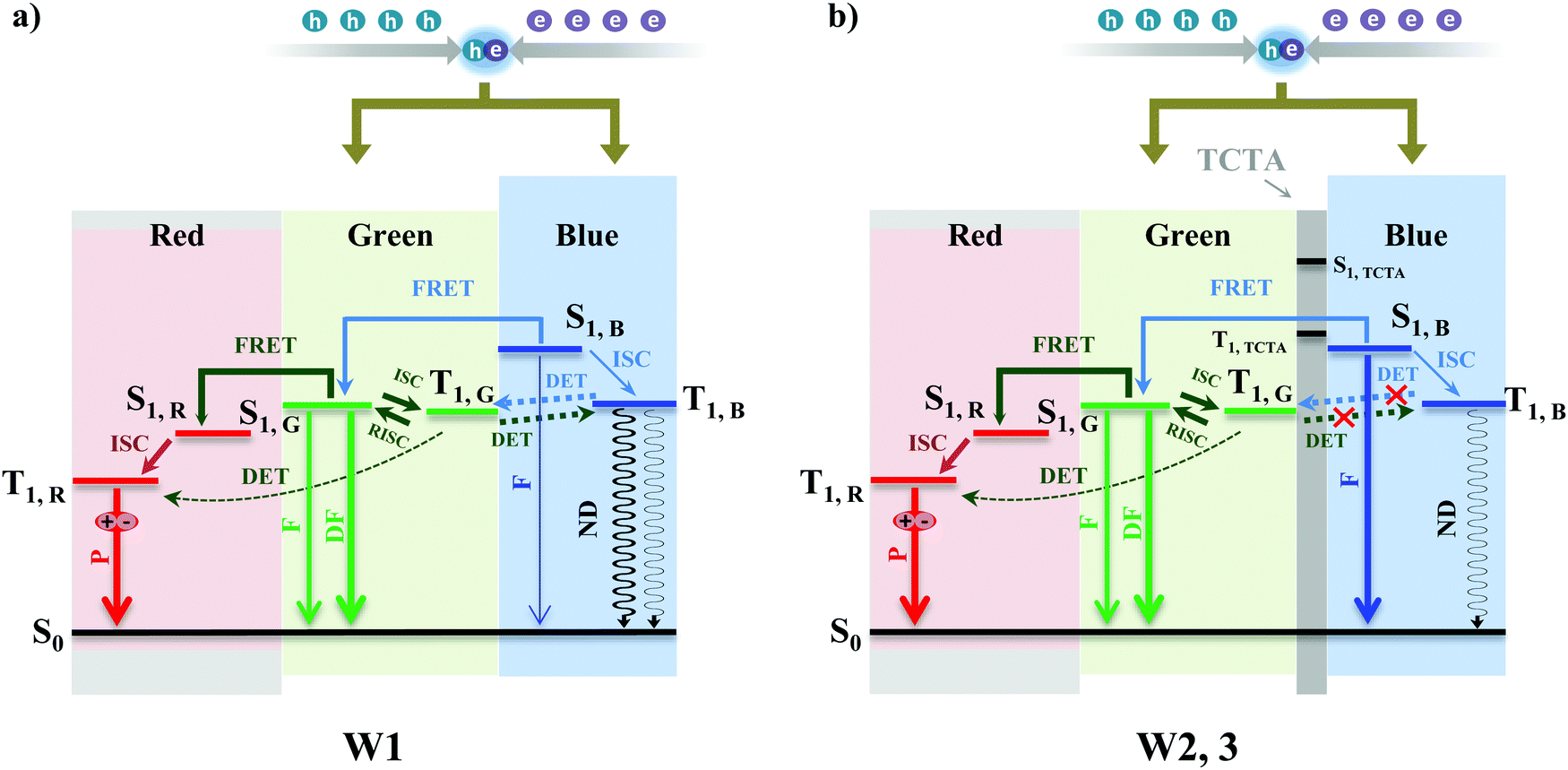 | ||
| Fig. 6 Working mechanisms of devices W1 (a) and W2 and W3 (b). Here, S1,B, S1,G, and S1,R are the singlet energy levels of TPB-AC, CP-BP-PXZ, and Ir(dmppr-mp)2(divm), respectively. T1,B, T1,G, and T1,R are the triplet energy levels of TPB-AC, and CP-BP-PXZ, and Ir(dmppr-mp)2(divm), respectively. FRET and DET are the Förster and Dexter energy transfer, respectively. P, F, DF, and ND are the phosphorescence, fluorescence, delayed fluorescence, and non-radiative decay, respectively. ISC and RISC are the intersystem crossing and the reverse intersystem crossing, respectively. | ||
3. Conclusions
We successfully fabricated high-performance hybrid white OLEDs by simply employing blue TPB-AC and green CP-BP-PXZ AIEgens as non-doped fluorophore emissive layers and red Ir(dmppr-mp)2(divm) doped TCTA as a phosphor emissive layer. The produced three-color hybrid WOLEDs simultaneously achieved high efficiencies (PEmax = 50.5 lm W−1, EQEmax = 20.5%), low roll-off (PEmax = 32.9 lm W−1, EQEmax = 18.9%), and high CRI (≥90). The mechanism investigation demonstrates that the direct carrier recombination, FRET and DET processes between the blue/green/red emitters, and the partial charge carrier trapping process on the red phosphor are three basic ways to achieve the hybrid white OLEDs. It can be seen that the introduction of the TCTA interlayer between the non-doped blue and green layers restrains the unfavorable DET processes and efficiently manages the exciton distribution to ensure the EL performance of the fabricated white OLEDs. Evidently, AIEgens are promising material systems to simply fabricate high-performance OLEDs, thus reducing costs for the applications of OLEDs in displays and lighting.4. Experimental section
Device fabrication and characterization
All of the devices were manufactured on clean glass substrates, which were pre-patterned with 180 nm thickness indium tin oxide (ITO) exhibiting a sheet resistance of 10 Ω per square. The ITO glass substrates were entirely cleaned by ultrasonic detergent and de-ionized bath progressively and then dried in a baking oven at 120 °C for 60 minutes to remove the residual solvent. Afterwards, the cleaned ITO substrates were treated by plasma for 4 minutes. Then they were transferred into the vacuum chamber for deposition. The pressure of the chamber was kept below 4 × 10⁻⁵ Pa with the help of a turbo pump. The transporting and light-emitting layers were deposited onto the ITO surface at a rate of 1–2 Å s−1, and the 1 nm thickness LiF layer was subsequently deposited onto the electron-transporting layer at a relatively low rate of 0.1–0.2 Å s−1 to act as the electron injection layer. At last, the 120 nm thickness Al layer as the cathode was deposited onto the LiF layer at a rate of 2–4 Å s−1. The fabricated devices exhibited an emitting area of 4 × 4 mm2 formed by the cross region of ITO and Al. The current density–luminance–voltage characteristics were measured using a Keithley 2400 and a Luminance Meter LS-110. The EL spectra were collected by an FlAME-S-VIS-NIR optical analyzer. The EQEs were calculated by considering a Lambertian emitter. The transient PL spectra of the films and the time-resolved EL spectra of device W2 were measured at a current density of 1 mA cm−2 using an Edinburgh Instruments F980 Spectrometer. The capacitance–voltage characteristics of devices C1–C3 and W2 were collected by an E4990A Impedance Analyzer at a frequency of 3000 Hz. All the measurements were carried out at room temperature under ambient laboratory conditions.Conflicts of interest
There are no conflicts of interest to declare.Acknowledgements
This work was supported by the National Natural Science Foundation of China (Grant No. 21788102, 91833304, 51527804) and Guangzhou Science & Technology plan project (201707020040).References
- Q. Sun, Y. Hu, Y. Dai and D. Ma, J. Mater. Chem. C, 2017, 5, 8022–8026 RSC.
- Y. Hu, T. Zhang, J. Chen, D. Ma and C.-H. Cheng, Isr. J. Chem., 2014, 54, 979–985 CrossRef CAS.
- N. Sun, Q. Wang, Y. Zhao, D. Yang, F. Zhao, J. Chen and D. Ma, J. Mater. Chem. C, 2014, 2, 7494–7504 RSC.
- F. Zhao, Y. Wei, H. Xu, D. Chen, T. Ahamad, S. Alshehri, Q. Pei and D. Ma, Mater. Horiz., 2017, 4, 641–648 RSC.
- Z. Wu, Q. Wang, L. Yu, J. Chen, X. Qiao, T. Ahamad, S. M. Alshehri, C. Yang and D. Ma, ACS Appl. Mater. Interfaces, 2016, 8, 28780–28788 CrossRef CAS PubMed.
- Z. Wu, J. Luo, N. Sun, L. Zhu, H. Sun, L. Yu, D. Yang, X. Qiao, J. Chen, C. Yang and D. Ma, Adv. Funct. Mater., 2016, 26, 3306–3313 CrossRef CAS.
- N. Sun, Q. Wang, Y. Zhao, Y. Chen, D. Yang, F. Zhao, J. Chen and D. Ma, Adv. Mater., 2014, 26, 1617–1621 CrossRef CAS PubMed.
- J. Chen, F. Zhao and D. Ma, Mater. Today, 2014, 17, 175–183 CrossRef CAS.
- Z. Wu, L. Yu, X. Zhou, Q. Guo, J. Luo, X. Qiao, D. Yang, J. Chen, C. Yang and D. Ma, Adv. Opt. Mater., 2016, 4, 1067–1074 CrossRef CAS.
- Q. Wang, J. Ding, D. Ma, Y. Cheng, L. Wang and F. Wang, Adv. Mater., 2009, 21, 2397–2401 CrossRef CAS.
- S. Gong, Y. Chen, J. Luo, C. Yang, C. Zhong, J. Qin and D. Ma, Adv. Funct. Mater., 2011, 21, 1168–1178 CrossRef CAS.
- Y. Sun, N. C. Giebink, H. Kanno, B. Ma, M. E. Thompson and S. R. Forrest, Nature, 2006, 440, 908–912 CrossRef CAS PubMed.
- S. Reineke, F. Lindner, G. Schwartz, N. Seidler, K. Walzer, B. Lussem and K. Leo, Nature, 2009, 459, 234–238 CrossRef CAS PubMed.
- D. Zhang, L. Duan, Y. Zhang, M. Cai, D. Zhang and Y. Qiu, Light: Sci. Appl., 2015, 4, e232 CrossRef CAS.
- J. Mei, Y. Hong, J. W. Lam, A. Qin, Y. Tang and B. Z. Tang, Adv. Mater., 2014, 26, 5429–5479 CrossRef CAS PubMed.
- J. Mei, N. L. Leung, R. T. Kwok, J. W. Lam and B. Z. Tang, Chem. Rev., 2015, 115, 11718–11940 CrossRef CAS PubMed.
- Z. Zhao, H. Nie, C. Ge, Y. Cai, Y. Xiong, J. Qi, W. Wu, R. T. K. Kwok, X. Gao, A. Qin, J. W. Y. Lam and B. Z. Tang, Adv. Sci., 2017, 4, 1700005 CrossRef PubMed.
- W. W. H. Lee, Z. Zhao, Y. Cai, Z. Xu, Y. Yu, Y. Xiong, R. T. K. Kwok, Y. Chen, N. L. C. Leung, D. Ma, J. W. Y. Lam, A. Qin and B. Z. Tang, Chem. Sci., 2018, 9, 6118–6125 RSC.
- X. Zhan, Z. Wu, Y. Lin, Y. Xie, Q. Peng, Q. Li, D. Ma and Z. Li, Chem. Sci., 2016, 7, 4355–4363 RSC.
- F. Song, Z. Xu, Q. Zhang, Z. Zhao, H. Zhang, W. Zhao, Z. Qiu, C. Qi, H. Zhang, H. H. Y. Sung, I. D. Williams, J. W. Y. Lam, Z. Zhao, A. Qin, D. Ma and B. Z. Tang, Adv. Funct. Mater., 2018, 28, 1800051 CrossRef.
- T. Liu, L. Zhu, C. Zhong, G. Xie, S. Gong, J. Fang, D. Ma and C. Yang, Adv. Funct. Mater., 2017, 27, 1606384 CrossRef.
- L. Chen, G. Lin, H. Peng, S. Ding, W. Luo, R. Hu, S. Chen, F. Huang, A. Qin, Z. Zhao and B. Z. Tang, Mater. Chem. Front., 2017, 1, 176–180 RSC.
- G. Lin, H. Peng, L. Chen, H. Nie, W. Luo, Y. Li, S. Chen, R. Hu, A. Qin, Z. Zhao and B. Z. Tang, ACS Appl. Mater. Interfaces, 2016, 8, 16799–16808 CrossRef CAS PubMed.
- Z. Xu, Y. Gong, Y. Dai, Q. Sun, X. Qiao, D. Yang, X. Zhan, Z. Li, B. Z. Tang and D. Ma, Adv. Opt. Mater., 2019, 1801539 CrossRef.
- J. Guo, X.-L. Li, H. Nie, W. Luo, S. Gan, S. Hu, R. Hu, A. Qin, Z. Zhao, S.-J. Su and B. Z. Tang, Adv. Funct. Mater., 2017, 27, 1606458 CrossRef.
- J. Guo, X.-L. Li, H. Nie, W. Luo, R. Hu, A. Qin, Z. Zhao, S.-J. Su and B. Z. Tang, Chem. Mater., 2017, 29, 3623–3631 CrossRef CAS.
- J. Guo, Z. Zhao and B. Z. Tang, Adv. Opt. Mater., 2018, 6, 1800264 CrossRef.
- R. Furue, T. Nishimoto, I. S. Park, J. Lee and T. Yasuda, Angew. Chem., Int. Ed., 2016, 55, 7171–7175 CrossRef CAS PubMed.
- J. Huang, H. Nie, J. Zeng, Z. Zhuang, S. Gan, Y. Cai, J. Guo, S.-J. Su, Z. Zhao and B. Z. Tang, Angew. Chem., Int. Ed., 2017, 56, 12971–12976 CrossRef CAS PubMed.
- H. Liu, J. Zeng, J. Guo, H. Nie, Z. Zhao and B. Z. Tang, Angew. Chem., Int. Ed., 2018, 57, 9290–9294 CrossRef CAS PubMed.
- G. Lin, L. Chen, H. Peng, S. Chen, Z. Zhuang, Y. Li, B. Wang, Z. Zhao and B. Z. Tang, J. Mater. Chem. C, 2017, 5, 4867–4874 RSC.
- Z. Xu, J. Gu, X. Qiao, A. Qin, B. Z. Tang and D. Ma, ACS Photonics, 2019, 6, 767–778 CrossRef CAS.
Footnote |
| † Electronic supplementary information (ESI) available. See DOI: 10.1039/c9qm00539k |
| This journal is © the Partner Organisations 2019 |