
 Open Access Article
 This Open Access Article is licensed under a
 Creative Commons Attribution 3.0 Unported Licence
Effect of hydrogen chloride etching on carrier recombination processes of indium phosphide nanowires†
Xiaojun
Su
ab,
Xulu
Zeng
c,
Hynek
Němec
d,
Xianshao
Zou
b,
Wei
Zhang
*a,
Magnus T.
Borgström
 c and
Arkady
Yartsev
*b
c and
Arkady
Yartsev
*b
aSchool of Physics and Electronic Engineering, Guangzhou University, Guangzhou 510006, China. E-mail: wzhang@gzhu.edu.cn
bChemical Physics and NanoLund, Lund University, Lund 22100, Sweden. E-mail: Arkady.Yartsev@chemphys.lu.se
cSolid State Physics and NanoLund, Lund University, Lund 22100, Sweden
dInstitute of Physics of the Czech Academy of Sciences, Prague 18221, Czech Republic
First published on 19th July 2019
Abstract
Introduction of in situ HCl etching to an epitaxial growth process has been shown to suppress radial growth and improve the morphology and optical properties of nanowires. In this paper, we investigate the dynamics of photo-generated charge carriers in a series of indium phosphide nanowires grown with varied HCl fluxes. Time resolved photo-induced luminescence, transient absorption and time resolved terahertz spectroscopy were employed to investigate charge trapping and recombination processes in the nanowires. Since the excitation photons generate charges predominantly in less than a half length of the nanowires, we can selectively assess the charge carrier dynamics at their top and bottom. We found that the photoluminescence decay is dominated by the decay of the mobile hole population due to trapping, which is affected by the HCl etching. The hole trapping rate is in general faster at the top of the nanowires than at the bottom. In contrast, electrons remain highly mobile until they recombine non-radiatively with the trapped holes. The slowest hole trapping as well as the least efficient non-radiative recombination was recorded for etching using the HCl molar fraction of χHCl = 5.4 × 10⁻⁵.
1. Introduction
Semiconductor nanowires have received intense interest as they have potential for application in photovoltaic cells,1–6 nanolasers,7,8 light-emitting diodes,9–12 field-effect transistors,13,14 sensors,15,16 and photodetectors.17,18 Significant efforts have been made for the manufacturing of high-quality materials, which are needed for device applications.19–22In situ etching allows for control over the axial and radial nanowire growth rate.23–26In situ etching of Indium Phosphide (InP) nanowires by the use of Hydrogen Chloride (HCl) was found to suppress radial growth and improve the morphology and photoluminescence (PL) of the nanowires.23,27 Furthermore, the HCl etching influences the nanowire surface morphology and reduces defect incorporation23,28 that occurs due to low temperature parasitic radial growth.23 Although this may affect carrier trapping and recombination processes together with the carrier mobility in the nanowires,14 the particular relationship between HCl etching and charge carrier dynamics in the nanowires is yet to be clarified.In this study, we examine the charge carrier dynamics in a series of in situ etched epitaxially grown InP nanowires. For this, we employ a combination of several time-resolved techniques:29,30 time-resolved terahertz spectroscopy (TRTS) and photoluminescence (TRPL) as well as femtosecond-transient absorption (TA) spectroscopy. This overcomes the possible limitations of each single technique and allows the obtaining of conclusive results. More specifically, TRTS probes mainly the population and mobility of the most mobile carriers, and TRPL monitors radiative recombination and is sensitive to the product of mobile electron and hole concentrations, whereas TA is sensitive to both radiative and non-radiative recombination processes. Thus, the combination of TRPL and TA enables us to distinguish between radiative and non-radiative recombination processes, the combination of TRTS and TRPL enables us to separate the mobile electron and hole dynamics, and the combination of TRTS and TA allows us to disentangle the temporal evolution of charge mobility and dynamics from the charge concentration. In this work, the results from TRPL, TA and TRTS together lead to the conclusion that the PL quenching represents the hole trapping process with a characteristic time constant which is dependent on the HCl molar fraction used. The recombination of the photogenerated charges is thus predominantly non-radiative. We also find that the HCl etching has almost no influence on the electron mobility over the first 200 ps. Since the excitation photons in our experiments are absorbed predominantly in the vicinity of the excitation incidence side of the nanowire array, we can distinguish charge carrier dynamics at the top and bottom of the nanowires: the hole trapping time is in general longer at the top of the nanowires than at the bottom. The slowest hole trapping and charge recombination in the entire series were observed for nanowires grown in the presence of an HCl molar fraction of 5.4 × 10⁻⁵.
2. Results and discussion
2.1. Nanowire morphology
InP nanowire arrays were grown on InP (111) B substrates by the use of metal organic vapor phase epitaxy (MOVPE).31–33 Six 1 × 1 cm2 InP nanowire arrays were grown with different molar fractions of HCl (χHCl) in the gas phase, ranging from 0 to 8.5 × 10⁻⁵, see Table 1. The resulting arrays consist of nanowires with a diameter of D = 200 nm and a length of L = 2.0 μm in a hexagonal pitch of 500 nm (Fig. 1). For part of the measurements, the nanowires were embedded in a colorless First Contact (FC) polymer film (Photonic Cleaning Technology LLC) and then removed from the native substrate together with the polymer by a peel off procedure. The polymer used is optically transparent and inert having an optical refractive index of ∼1.5, exhibiting no response to either of the measurements. In particular, this procedure eliminates the otherwise dominating THz photoconductivity of the bulk InP substrate, while basically maintaining the regular structure of the nanowire array. Despite the upside-down reversal during the embedding, we will stick to the convention that the “bottom” side of the nanowire is where an InP nanowire was attached to the InP substrate, while the “top” side is the opposite one (ESI 1†). The morphology of the as-grown nanowires was investigated by electron microscopy (SEM and TEM). The SEM images reveal that the nanowires without HCl etching start kinking during the growth when the length of the nanowires is approaching 1 μm and that the surface of the nanowires is rather rough, indicating a large number of structural defects. With increasing HCl molar fraction χHCl, the nanowire kinking gradually disappears with the increase of the HCl molar fraction to 3.9 × 10⁻⁵ (Fig. 1). The reason that HCl reduces the kinking is twofold: (1) the effective ratio of In and P atoms changes when HCl is introduced due to chlorination of TMIn; (2) HCl affects the surface energy of the particle and leads to different vapor–liquid, vapor–solid and possibly liquid–solid interfacial energies, which may result in a more stable particle on top of the nanowire.23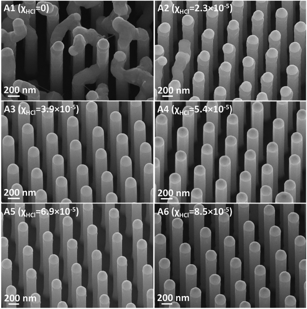 | ||
| Fig. 1 SEM images of the InP nanowires grown with different HCl molar fractions. The images were recorded at an angle of 30° toward the normal plane of the substrate. | ||
| HCl molar fraction | As-grown sample | Polymer-embedded sample | |
|---|---|---|---|
| χ HCl (10−5) | Top | Bottom | |
| 0 | A1 | T1 | B1 |
| 2.3 | A2 | — | — |
| 3.9 | A3 | — | — |
| 5.4 | A4 | T4 | B4 |
| 6.9 | A5 | — | — |
| 8.5 | A6 | T6 | B6 |
2.2. Excitation beam propagation
We have calculated the light in-coupling in a periodic array of nanowires embedded in the polymer using the finite element method (COMSOL, Multi-physics),34–36 see Fig. 2. For the excitation at 800 nm, the absorption length is about 0.25 μm; however, due to waveguiding, the initial excitation density is concentrated to the interior of the nanowires, within ∼0.5 μm from the excitation side. The excitation pattern at 400 nm is more complex. The penetration depth is within the tens of nm range; the highest initial excitation density is thus at the very top of the nanowire. More importantly, due to the waveguiding in the nanowire arrays, the major part of the excitation density distributes around the surface of the nanowire (this effect is only hardly seen as the slightly lighter colour in the right side of the corresponding quarter-segment in Fig. 2). | ||
| Fig. 2 Distribution of the excitation density (number of photons absorbed in a unit volume) shown for a quarter segment of a nanowire induced by 800 and 400 nm polarized light pulses. Excitation density is calculated in an array of nanowires embedded in the completely transparent polymer matrix. The graph shows a cumulative fraction of the radiation absorbed up to the given depth. The selected quantiles are emphasized by white curves. For the employed excitation wavelengths of 400 and 800 nm, ∼80% of the radiation is absorbed within approximately a half-length of the nanowire. | ||
After excitation, one has to consider the diffusion of mobile carriers that homogenize the carrier density over the nanowires on long time scales. The impact of these processes can be estimated from the ambipolar diffusion length LD = (DAt)1/2, where DA = 2DeDh/(De + Dh) = 10 cm2 s−1 is the ambipolar diffusion coefficient of InP.37 We obtain, e.g., LD = 100 nm in 10 ps; 320 nm in 100 ps and 1000 nm in 1 ns. This has two important implications: (i) charges are distributed rather homogeneously across the nanowire in about ten picoseconds (the diffusion coefficient for lateral diffusion in InP nanowires is close to the bulk one37) and (ii) diffusion is too slow to cause homogenization of the carrier density along the nanowire on a nanosecond time scale (the diffusion along the nanowire is in fact even slower than that in the bulk, due to the presence of stacking faults).14,38 Furthermore, as will be shown below, photogenerated holes are trapped on the time scale of a few hundreds of ps, which essentially prevents further ambipolar diffusion.
The homogenization across the nanowire implies that a good estimate of the charge density at short times (10–300 ps) is an integral over the circular cross-section, which is a function of the nanowire length (Fig. 2). Despite the completely different initial excitation profiles, we see that these homogenized profiles are almost the same, with the majority of excitation densities concentrated in the top half of the nanowire. By exciting the nanowire array from the top and the bottom, it is thus possible to selectively study the carrier dynamics at different locations of the nanowire.
2.3. TRPL dynamics
All the as-grown InP nanowire arrays under 400 nm excitation display a PL emission peak at ∼1.34 eV, which is very close to the Zinc Blende InP band-gap.39,40 To examine the effect of the HCl etching on carrier recombination dynamics, we analyzed the kinetics of the spectrally integrated TRPL in both the as-grown nanowires and the nanowires embedded in the polymer matrix (Fig. 3). The PL decay is qualitatively similar in both types of samples: this suggests that the nanowire photo-physics is nearly unaffected by the presence of the polymer. The PL decay is the slowest for the nanowires grown in the presence of a HCl molar fraction of χHCl = 5.4 × 10⁻⁵, whereas it speeds up as the HCl molar fraction becomes more distant from this optimum value (the PL decay time obtained by fitting of the kinetics shown in Fig. 3(a) is given in ESI 2†).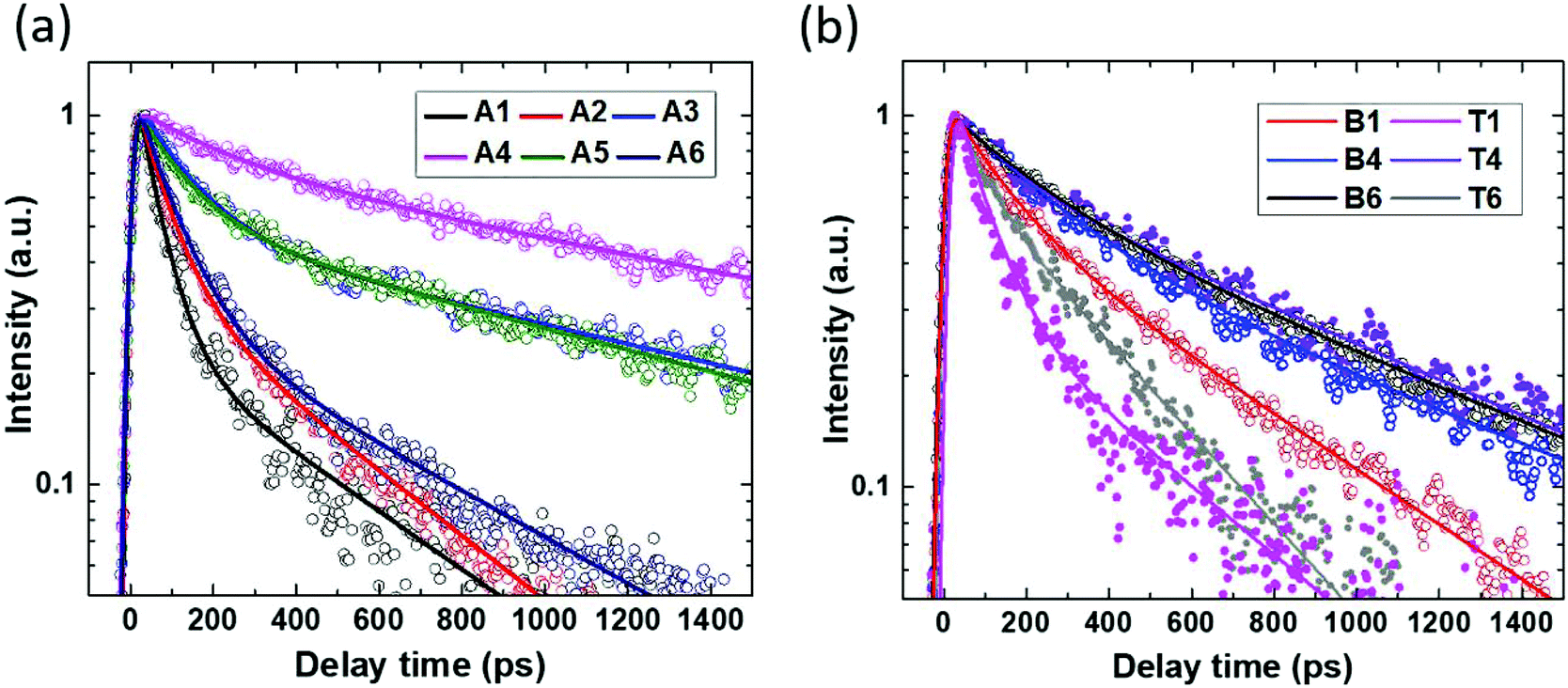 | ||
| Fig. 3 (a) Spectrally integrated PL kinetics of InP nanowire arrays grown with different HCl molar fractions A1–A6 after photoexcitation at 400 nm. The excitation photon flux was 9 × 10¹¹ photons per cm2 per pulse. (b) Spectrally integrated PL kinetics of InP nanowire arrays embedded in the polymer, after photoexcitation at 780 nm of the top (T) and bottom (B) of the nanowire arrays. The labelling is according to Table 1. Symbols: measurements. Closed and open symbols correspond to the kinetics for the Top or the Bottom of the nanowire arrays, respectively. Lines: fits by bi-exponential decay functions; the fitting parameters can be found in Tables ST1 and ST2 in ESI 2.† | ||
Conventionally, radiative recombination of mobile charge carriers in semiconductors is considered as a bimolecular (second order) process. A non-radiative process of Auger recombination leads to a third-order component in the decay of charge concentration. Furthermore, mobile charges can be trapped by surface states, impurities and defects, which would prevent their radiative recombination and will appear as a first order process in PL decay. The distinction between these processes can be achieved via the variation of the excitation density by changing the excitation fluence. In this study, decreasing the excitation fluence two times causes only marginal changes in the TRPL kinetics (Fig. 4). This implies that the second and third order processes are negligible at the employed excitation levels: for example, when the excitation is increased two times the radiative recombination if dominant should increase PL decay rates by a factor of 2 (and even by a factor of 4 in the case of dominant Auger recombination). We thus conclude that charge trapping—which is a first order, intensity-independent process—is dominating the PL decay.
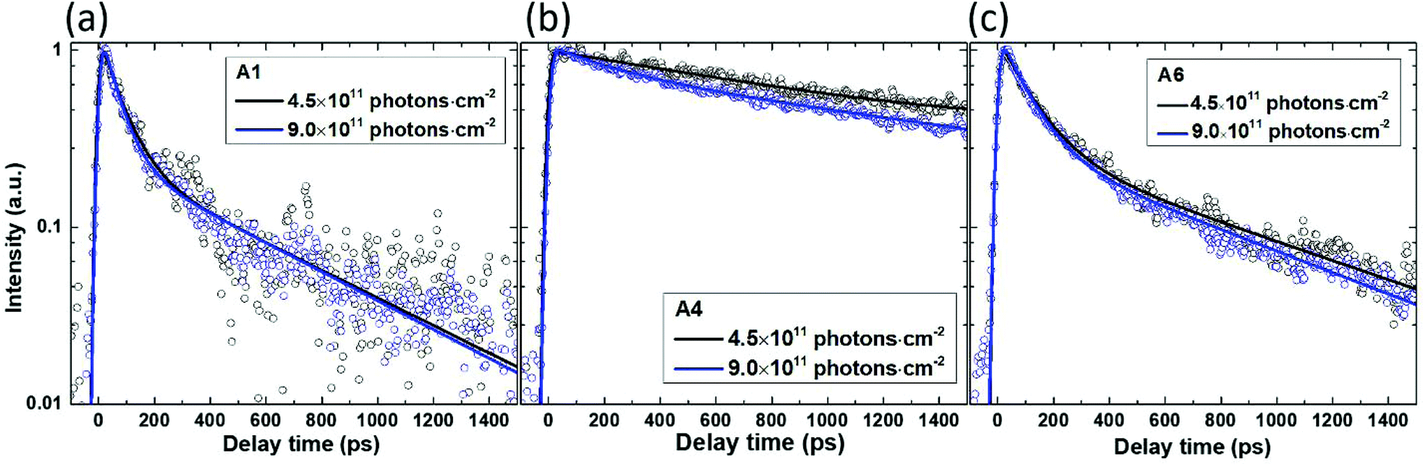 | ||
| Fig. 4 Spectrally integrated TRPL decays of the as-grown InP nanowires with HCl molar fractions of (a) χHCl = 0 (A1), (b) 5.4 × 10⁻⁵ (A4) and (c) 8.5 × 10⁻⁵ (A6) during the nanowire growth under excitation at 400 nm at the indicated excitation densities. Symbols: measurements (the intensities are normalized by the excitation power). Lines: fits by bi-exponential decay functions; the fitting parameters can be found in Table ST3 in ESI 2.† | ||
The only exception is the nanowire grown with χHCl = 5.4 × 10⁻⁵, for which the decay becomes slightly faster at higher excitation intensity (as shown in Fig. 4(b)), suggesting a possible minor contribution of the radiative second-order recombination. This decay channel may be visible due to the slower charge trapping rate in these nanowires (about ten times slower TRPL decay judged by the 1/e amplitude decrease).
We note here that in contrast to the expected single exponential decay for TRPL dynamics being dominated by a charge trapping, we always observe essentially bi-exponential PL decays (see Tables ST1 and ST2 in ESI 2†). This type of excitation-independent dynamics may be associated with a distribution of trapping rates. The bi-exponential decay together with a considerable difference between the slow and fast decay constants thus indicates the presence of trap states of two different characteristics, responsible for fast and slow charge trapping.
In the discussion so far, we neglected the role of an unintentional doping concentration N0,41 which would lead to an enhanced recombination. To justify this approach, we estimated the density of photogenerated charges with the assumption that all absorbed photons are converted into electrons and holes. As the absorption of the polymer is negligible, the excitation is entirely absorbed by the nanowires29 and the mean concentrations of the photo-generated charges averaged over the entire volume of nanowires are 7 × 10¹⁶ and 1.4 × 1017 cm−3, respectively, in the TRPL experiments for the excitation fluences from Fig. 4. Furthermore, the excitation generates more than half of the charges in the first quarter of nanowires, and therefore the characteristic charge concentration is about 2 times higher than the averaged values given above. The concentration of photogenerated charges is thus considerably higher than the unintentional doping concentration N0, which is expected at the level of ∼1016 cm−3.42,43 There is thus no need to further revise the interpretation of the TRPL results.
As shown in Fig. 3(b), the TRPL decay does not depend on the excitation orientation of samples T4 and B4. We associate this observation with the uniform trap density along the nanowires. In contrast, the PL decay rate depends on the excitation orientation for other HCl fluxes, suggesting that in those cases the traps are distributed unevenly along the nanowire length. Thus, based on the TRPL results, we identify an optimum χHCl = 5.4 × 10⁻⁵ within the available set of nanowires that leads to the lowest and homogeneously distributed density of traps.
Since radiative recombination and consequently the PL emission depend on the product of mobile electron and hole concentrations,44,45 both electron and hole trapping may influence the PL decay. Hence, based solely on TRPL measurements, we cannot a priori distinguish whether electrons or holes or both are trapped.
2.4. THz photoconductivity kinetics
In InP, TRTS probes electrons selectively, as their mobility is considerably higher than that of the holes due to the difference in effective masses.45–48 We first verified that the normalized transient THz transmittance kinetics are intensity-independent even under excitation fluences of 2.1 × 10¹² and 4.6 × 10¹² photons per cm2 per pulse, which are significantly higher than those in TRPL measurements, but which are required to obtain a measurable signal in TRTS (ESI 3†). We can thus rule out the bimolecular and Auger recombination at these excitations and thus correlate the TRTS measurements with the conclusions based on the TRPL results.Similar to the case of PL, the decay of the THz signal is the slowest for sample B4 and it becomes faster for the other HCl molar fractions. The transient THz transmittance decay in the etched nanowires is nearly independent of the excitation direction (ESI 4†); nevertheless in nanowires grown without the presence of HCl the decay is faster when excited from the top (T1) than from the bottom (B1) as shown in Fig. 5(b). We correlate this difference with the nanowire morphology. According to the SEM images (Fig. 1), the nanowires grown without etching have a highly irregular shape on the top side, which may lead to different transient THz photoconductivity from that in the rest of the nanowires. The faster decay of the THz kinetics measured when exciting from the top side of the nanowires most probably indicates that charges photo-generated in the irregularly grown part are more rapidly trapped as compared to the rest of the nanowire.
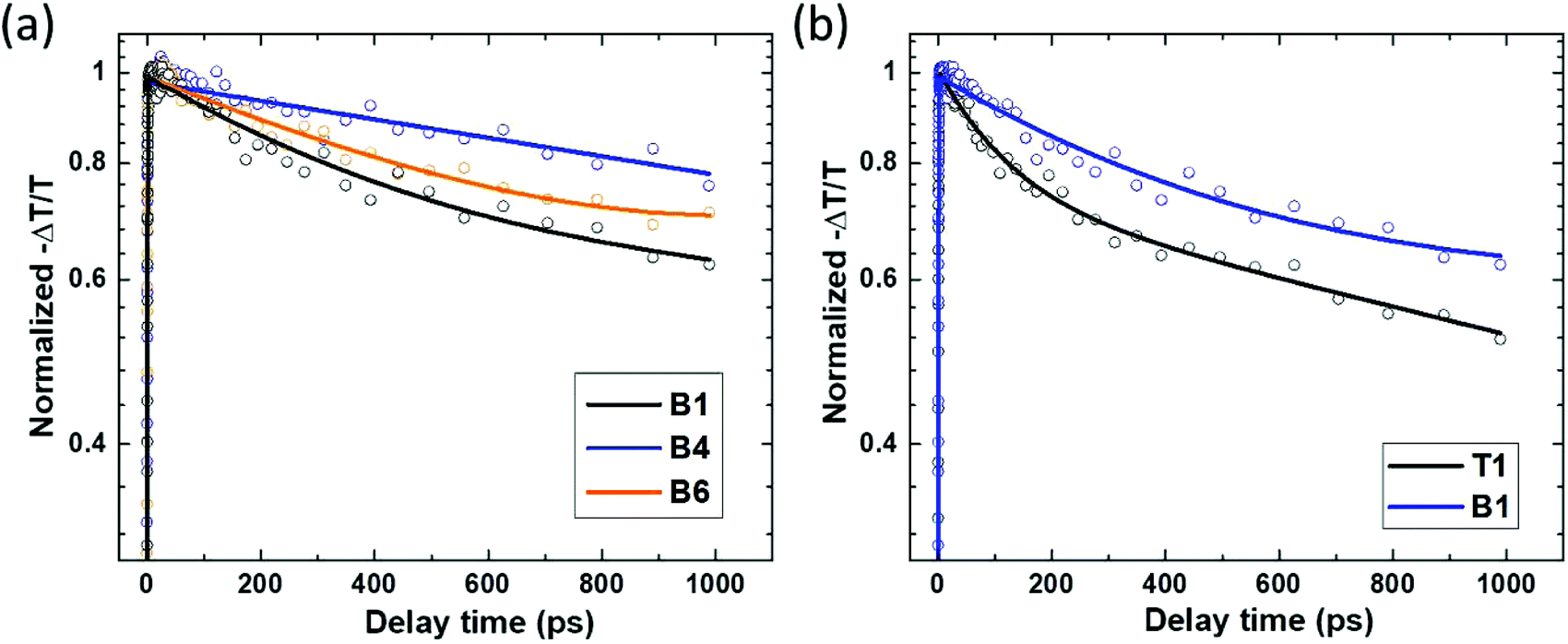 | ||
| Fig. 5 Normalized transient THz transmittance kinetics of the selected InP nanowire arrays embedded in the polymer, excited at 800 nm with the flux of 4.6 × 10¹² photons per cm2 per pulse. (a) Excitation from the bottom side. (b) Comparison of the signal upon excitation from the top and bottom sides of the sample prepared without HCl etching. Symbols: measurements. Lines: bi-exponential fits. The fitting parameters can be found in Tables ST4 and ST5 in ESI 3 and 4.† | ||
From the TRTS measurements, we can extract the photoconductivity of the series of InP nanowires and estimate the charge mobility μ via dividing the measured (effective) conductivity Δσ by the number of photo-generated charge carriers eNexc at early delay time (ESI 5†). We found that at very low excitation fluence at 400 nm the charge mobility is ∼2200 cm2 V−1 s−1 and that the HCl etching has a negligible influence on this value, see Fig. 6. This value is comparable with the electron mobility but is much higher than the reported hole mobility in InP.36 We thus prove that the THz photoconductivity is dominated by electrons. The dependence of THz photoconductivity decay on HCl etching appears to be less pronounced with excitation at 400 nm compared to that at 800 nm, as shown in Fig. 5, which may be related to the difference in excitation density distribution at two excitation wavelengths.
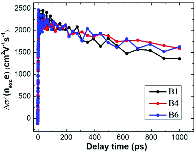 | ||
| Fig. 6 Evolution of THz photoconductivity normalized by initial charge density under the excitation at 400 nm with the density of 2.3 × 10¹¹ photons per cm2 per pulse. | ||
The simple mobility estimate based just on the expression Δσ/(eNexc) has to be considered very cautiously as it is—strictly speaking—valid only in bulk materials. The normalized effective conductivity is generally dependent on excitation density in heterogeneous systems (Fig. 6) and the primary reason is the effect of depolarization fields, which are inherently induced in non-percolated heterogeneous systems.49 According to the developed formalism and in relation to the photoconductivity measurements in this study, only the value at the lowest excitation intensities represents the true mobility of charges.
2.5. Transient absorption and synthesis of results
TA reveals the decay of the overall photo-generated charge carrier population in the material, due to both radiative and non-radiative recombination and is in general insensitive to the charge mobility.The kinetics of TA and the other two time-resolved techniques for the nanowires grown under optimal conditions (χHCl = 5.4 × 10⁻⁵) are shown in Fig. 7(a). The TA decays negligibly slower than the transient THz transmittance, whereas the decay of PL is obviously the fastest. The same behaviour was also observed in the other samples (ESI 6†). The longest decay (TA and TRPL) is interpreted as recombination dynamics, occurring on a nanosecond time scale. Further, if a significant part of photo-generated charges recombines radiatively, in TA we have to observe the same kinetics as in TRPL, with the amplitude proportional to the part of charges recombining radiatively. As TA kinetics do not display any pronounced decay components identical to the dynamics of TRPL, we have to conclude that non-radiative recombination is the dominant channel of the overall recombination of photo-generated charges. This conclusion is also supported by the value of the absolute PL quantum yield (QY) of ∼5 × 10⁻⁴ as measured by the use of an integrating sphere (see the Experimental section). Fig. 7(a) thus implies that most photo-charges remain in the nanowires long after the radiative recombination decay is over and therefore recombine non-radiatively. From THz photoconductivity measurements, we concluded that the long-lived mobile charges are electrons. TRTS and TA kinetics are largely similar, and thus we conclude that the mobility of electrons does not change on the nanosecond time scale. Consequently, TRPL dynamics is dominated by the hole trapping. It is interesting to note that the HCl etching affects the non-radiative recombination rate qualitatively similar to the hole trapping, namely, that the TRTS and TA decay rates follow a similar trend to TRPL regarding the HCl etching condition, and the scheme of the charge carrier recombination processes is shown in Fig. 7(b).
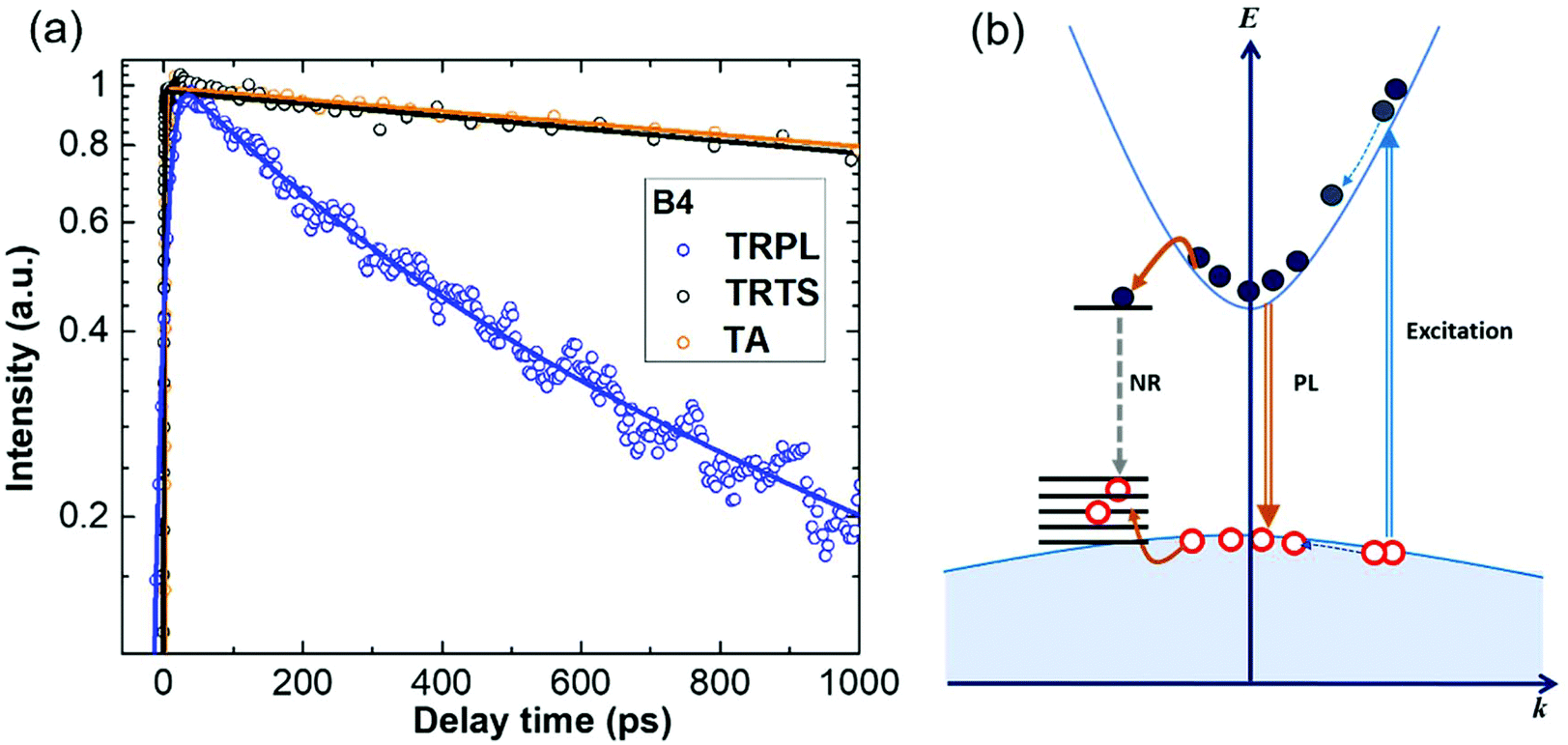 | ||
| Fig. 7 (a) Comparison of transient THz transmittance, TRPL and TA (all normalized to the peak value) in InP nanowires B4. Symbols: measurements. Solid lines represent the exponential fits; see the fitting parameters in Table ST6 in ESI 6.† (b) Scheme of charge carrier recombination processes in HCl in situ etched InP nanowires. Double curved lines represent the photoexcitation and emission processes; dark yellow curved lines represent the carrier trapping processes; dotted curved lines represent the charge relaxation processes; ‘NR’ represents the nonradiative recombination process; straight horizontal lines represent the trap states. | ||
We now return to the weak but pronounced excitation dependence observed in TRPL for the χHCl = 5.4 × 10⁻⁵ sample, as shown in Fig. 4(b). From TRTS data, in ESI Fig. S3,† we find that the photo-generated electron concentration in these nanowires does not undergo any substantial decay due to bimolecular or Auger recombination up to an excitation fluence of ∼1012 photons per cm2 per pulse. The observed dependence in TRPL measurements is thus related entirely to the hole trapping dynamics. Since the fast PL decay component nearly vanishes at the elevated intensity, we associate that dynamics with trap filling:29 traps become fully occupied at higher excitation intensities, thus closing the fast trapping channel. Now, assuming that in the nanowires grown with χHCl = 5.4 × 10⁻⁵ excited at 400 nm with 4.5 × 10¹¹ photons per cm2 per pulse the fast trapping channel is saturated, we can estimate the density of the fast trap states. For the average distance between the fast trapping states, we get ∼24 nm if the traps are distributed in the nanowire volume (trap density of ∼7 × 1016 cm−3) and ∼15 nm (trap density of ∼4 × 1011 cm−2) if the traps are located at the nanowire surface. As we did not see any trapping saturation in the other nanowires, we infer that the trap density in those nanowires is higher.
To further identify the nature of the hole traps, we analyzed the crystal structure and the surface quality (or the surface axial roughness as defined in ESI 7†) of the nanowires A1, A4 and A6 by transmission electron microscopy (TEM), as shown in Fig. 8. SAED patterns of the nanowires grown at χHCl values of 0, 5.4 × 10⁻⁵ and 8.5 × 10⁻⁵ are provided in ESI 8.† There appear to be less stacking faults at the top of the nanowires than at the bottom, see Table ST7 in ESI 7.† However, the PL quenching (dominated by the hole trapping) is more pronounced at the top side of the nanowires. Furthermore, the stacking fault density is the lowest in the bottom of the nanowires grown without etching, whereas the PL decay in these nanowires is the fastest. Therefore, we argue that there is no direct correlation between the stacking faults and the hole trapping in these nanowires.
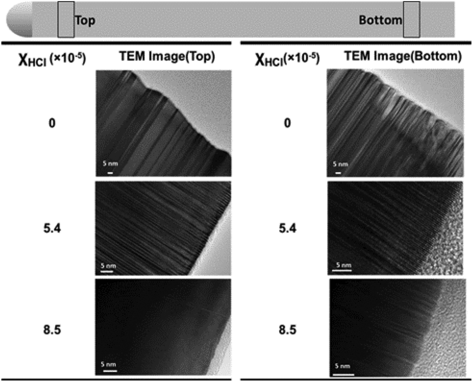 | ||
| Fig. 8 TEM images of the InP nanowire with HCl etching of χHCl = 0 (A1), χHCl = 5.4 × 10⁻⁵ (A4) and χHCl = 8.5 × 10⁻⁵ (A6) at the top and bottom of the nanowires. The top position was chosen away from the neck region and the bottom – away from the nanowire break region. | ||
Further we examined the surface of nanowire grown with different χHCl values and observe a pronounced reduction of the surface defect density at a χHCl value of 5.4 × 10⁻⁵; some surface defects on the bottom of the nanowires A6 and surface defects all over the nanowires grown without HCl etching are observed (see the method of quantification and the result in Table ST7 in ESI 7†). In particular, we observe a single obvious irregularity on the nanowire surface over ∼20 and ∼30 nm spans in ESI Fig. S7-1(a) and (b),† respectively, in agreement with the estimation of 15 nm for the average distance between traps.
Summarizing the analysis of the TEM data, we conclude that not-stacking faults, but surface related defects are essential for the hole trapping.
In this study, we demonstrate a pronounced reduction of carrier trapping of InP nanowire when regulating the InP nanowire growth by HCl etching. Our observation of the predominantly non-radiative recombination of photogenerated charges even at the optimal HCl etching indicates that surface passivation could be developed, thus allowing further improvements of prospective nanowire-based devices. It is important to note though that the optimization of carrier recombination has to be appropriately characterized via a thorough examination of the charge carrier dynamics and via absolute measurements of the photoluminescence quantum yield (or both) rather than by means of a relative increase of the PL intensity.
3. Experimental
3.1. InP nanowire growth
InP: Zn (111) B substrates were prepared by depositing Au particles in hexagonal arrays of holes with a diameter of 200 nm and a pitch of 500 nm by the use of nanoimprint lithography (NIL),50 metal evaporation and lift-off. The Au particles have a thickness of approximately 65 nm. The samples were grown in a low-pressure (100 mbar) metal organic vapor phase epitaxy (MOVPE) system (Aixtron 200/4) using Hydrogen (H2) as a carrier gas with a total flow of 13 l min−1. The sample was first heated to 280 °C for 1 min as a pre-anneal nucleation step for pattern preservation with trimethylindium (TMIn) and PH3 molar fractions of 8.9 × 10⁻⁵ and 6.92 × 10⁻³, respectively. These samples were then heated to an elevated temperature of 550 °C for 10 minutes in the mixed PH3/H2 atmosphere to desorb surface oxides. After this step, the temperature was set to 440 °C, and the growth was initiated by introducing trimethylindium (TMIn) and phosphine (PH3) at molar fractions of χTMIn = 7.4 × 10⁻⁵ and χPH3 = 6.92 × 10⁻³ to nucleate the nanowires. For samples grown with different HCl molar fractions of χHCl = 0, 2.3 × 10⁻⁵, 3.9 × 10⁻⁵, 5.4 × 10⁻⁵, 6.9 × 10⁻⁵, 8.5 × 10⁻⁵, Hydrogen Chloride (HCl) was introduced after a 15 s nucleation step to eliminate any radial growth. The nanowire length was in situ monitored by using reflectance spectroscopy. When the nanowire length reached 2 μm, the growth was finished by switching off the TMIn and HCl supply simultaneously while cooling down the reactor in a PH3/H2 atmosphere.3.2. Time-resolved photoluminescence (TRPL) measurements
TRPL was measured using a setup described in ref. 51. A Ti:Sapphire fs oscillator (∼100 fs, Spectra-Physics, Tsunami) at ∼780 nm or a frequency-doubled (400 nm) s-polarized (perpendicular to the nanowire axis) light was used for excitation. For the as-grown nanowires, the incident angle of the excitation beam was close to the Brewster angle (∼70°), and the samples were kept in N2. For the nanowires embedded in the FC film, the light propagates along the nanowire axis. PL was collected by two quartz plano-convex lenses and focused on the input slit of a spectrograph (Chromex). The output of the spectrograph was sent into the streak camera (Hamamatsu C6860). Efforts were made to maintain the alignment of the experimental set-up the same for all the samples studied. The measurements were performed at room temperature.3.3. Time-resolved terahertz spectroscopy (TRTS)
The terahertz setup was driven by a regenerative amplifier (Spitfire Pro XP, Spectra Physics) delivering 80 fs laser pulses with a central wavelength of 800 nm and a repetition rate of 1 kHz. The laser beam was split into three parts. The first branch (400 μJ per pulse) served for generation of intense THz pulses by tilted wave front optical rectification in a MgO![[thin space (1/6-em)]](https://www.rsc.org/images/entities/char_2009.gif) :LiNbO3 crystal. The second—much weaker—part was used for electro-optical sampling of the THz pulses in a 1 mm thick (110) ZnTe crystal. The third beam was employed for sample excitation: using either the fundamental (800 nm) or second harmonic (400 nm). Neutral density filters were used to attenuate the excitation intensity. The setup was purged with dry nitrogen to eliminate water vapor absorption. The measurements were performed at room temperature.
:LiNbO3 crystal. The second—much weaker—part was used for electro-optical sampling of the THz pulses in a 1 mm thick (110) ZnTe crystal. The third beam was employed for sample excitation: using either the fundamental (800 nm) or second harmonic (400 nm). Neutral density filters were used to attenuate the excitation intensity. The setup was purged with dry nitrogen to eliminate water vapor absorption. The measurements were performed at room temperature.
3.4. Time resolved transient absorption (TA) spectroscopy
TA signals were measured using a setup described in ref. 52, driven by a regeneratively amplified, mode-locked Yb:KGW (Ytterbium-doped potassium gadolinium tungstate) based femtosecond laser system (Pharos, Light conversion) operating at 1030 nm and delivering pulses of 200 fs at a repetition rate of 2 kHz. This laser is used to pump two non-collinearly optical parametric amplifiers (NOPAs, Orpheus-N, Light Conversion). One of them was used to generate pump pulses centred at 540 nm with a pulse duration of 35 fs. The second NOPA was used to generate probe pulses of about 40 fs duration in the spectral region from 900 nm to 930 nm for differential absorption measurements. The probe was time delayed with respect to the pump by a mechanical delay stage. The measurements were performed at room temperature.3.5. Absolute PL quantum yield (QY) measurement
We have measured the absolute PL quantum yield (QY) in the as-grown InP nanowire array by the integrating sphere method. We used a CW laser (780 nm) to excite the sample, an integrating sphere (HORIBA, Quanta-φ, F3029) for collection of the residual excitation light and the overall PL and a spectrometer (AvaSpec-ULS2048-USB2-UA-50) to detect the PL output. We have calculated the PL QY via accounting for the numbers of emitted and absorbed photons. Correction for the predominant out-coupling of the PL by the substrate has been performed according to ref. 53 and resulted in a factor of 4.5 for the given geometry of the nanowire arrays. At the excitation flux equivalent to ∼10 suns, we have obtained QY to be ∼4 × 10⁻⁴ for the as-grown InP nanowires with χHCl = 3.9 × 10⁻⁵. The measurements were performed at room temperature.3.6. Electron microscopy
Scanning electron microscopy (SEM) was performed using a Zeiss LEO 1560 setup equipped with a field emission electron emitter and operated at 10 kV. For transmission electron microscopy (TEM) measurements, nanowires were mechanically transferred onto lacey carbon film covered Cu-grids and investigated using a JEOL-3000F transmission electron microscope operated with a field emission gun at 300 kV.4. Conclusions
We employed a combination of time resolved terahertz spectroscopy, time resolved photoluminescence and transient absorption spectroscopy to investigate carrier dynamics in InP nanowires grown under different HCl etching conditions. We conclude that photo-generated charge carriers in these nanowires recombine predominantly non-radiatively on nanosecond time scales. Hole trapping is a much faster process that is dependent on HCl etching flux, reaching its lowest value at the HCl molar faction of 5.4 × 10⁻⁵. In contrast to holes, photo-generated electrons remain highly mobile until they recombine non-radiatively with the trapped holes. We observe that the hole trapping at the top of the nanowires is more efficient than that at the bottom, whereas electron dynamics is less sensitive to the position where they are generated. The hole traps are found to be mainly related to surface defects.Conflicts of interest
There are no conflicts to declare.Acknowledgements
This work was supported by the NanoLund at Lund University, Knut and Alice Wallenberg Foundation, Crafoord Foundation, Swedish Energy Agency, Swedish Research Council, PhD4Energy, China Scholarship Council, Czech Science Foundation (Grant 17-03662S), Operational Programme Research, Development and Education financed by European Structural and Investment Funds and the Czech Ministry of Education, Youth and Sports (Project No. SOLID21- CZ.02.1.01/0.0/0.0/16_019/0000760).References
- J. Wallentin, N. Anttu, D. Asoli, M. Huffman, I. Aberg, M. H. Magnusson, G. Siefer, P. Fuss-Kailuweit, F. Dimroth, B. Witzigmann and H. Q. Xu, Science, 2013, 339, 1057–1060 CrossRef CAS PubMed.
- I. Åberg, G. Vescovi, D. Asoli, U. Naseem, J. P. Gilboy, C. Sundvall, A. Dahlgren, K. E. Svensson, N. Anttu, M. T. Björk and L. Samuelson, IEEE J. Photovolt., 2016, 6, 185–190 Search PubMed.
- Y. Cui, J. Wang, S. R. Plissard, A. Cavalli, T. T. T. Vu, R. P. J. Van Veldhoven, L. Gao, M. Trainor, M. A. Verheijen, J. E. M. Haverkort and E. P. A. M. Bakkers, Nano Lett., 2013, 13, 4113–4117 CrossRef CAS PubMed.
- N. P. Dasgupta and P. D. Yang, Front. Phys., 2014, 9, 289–302 CrossRef.
- H. Goto, K. Nosaki, K. Tomioka, S. Hara, K. Hiruma, J. Motohisa and T. Fukui, Appl. Phys. Express, 2009, 2, 35004 CrossRef.
- G. Otnes, E. Barrigón, C. Sundvall, K. E. Svensson, M. Heurlin, G. Siefer, L. Samuelson, I. Åberg and M. T. Borgström, Nano Lett., 2018, 18, 3038–3046 CrossRef CAS PubMed.
- M. H. Huang, S. Mao, H. Feick, H. Yan, Y. Wu, H. Kind, E. Weber, R. Russo and P. D. Yang, Science, 2001, 292, 1897–1899 CrossRef CAS PubMed.
- Z. C. Wang, B. Tian, M. Pantouvaki, W. M. Guo, P. Absil, J. Van Campenhout, C. Merckling and D. Van Thourhout, Nat. Photonics, 2015, 9, 837–842 CrossRef CAS.
- X. Duan, Y. Huang, Y. Cui, J. Wang and C. M. Lieber, Nature, 2001, 409, 66–69 CrossRef CAS PubMed.
- F. Qian, S. Gradecak, Y. Li, C. Y. Wen and C. M. Lieber, Nano Lett., 2005, 5, 2287–2291 CrossRef CAS PubMed.
- J. Bao, M. A. Zimmler, F. Capasso, X. Wang and Z. F. Ren, Nano Lett., 2006, 6, 1719–1722 CrossRef CAS PubMed.
- R. Agarwal and C. M. Lieber, Appl. Phys. A: Mater. Sci. Process., 2006, 85, 209–215 CrossRef CAS.
- S. De Franceschi, J. A. Van Dam, E. P. A. M. Bakkers, L. F. Feiner, L. Gurevich and L. P. Kouwenhoven, Appl. Phys. Lett., 2003, 83, 344–346 CrossRef CAS.
- J. Wallentin, M. Ek, L. R. Wallenberg, L. Samuelson and M. T. Borgström, Nano Lett., 2012, 12, 151–155 CrossRef CAS PubMed.
- F. Patolsky, G. Zheng and C. M. Lieber, Nanomedicine, 2006, 1, 51–65 CrossRef CAS PubMed.
- P. Ambhorkar, Z. Wang, H. Ko, S. Lee, K. I. Koo, K. Kim and D. I. Cho, Micromachines, 2018, 9, 679 CrossRef PubMed.
- J. Wang, M. S. Gudiksen, X. Duan, Y. Cui and C. M. Lieber, Science, 2001, 293, 1455–1457 CrossRef CAS PubMed.
- C. J. Novotny, E. T. Yu and P. K. L. Yu, Nano Lett., 2008, 8, 775–779 CrossRef CAS PubMed.
- M. D. Stiles and D. R. Hamann, Phys. Rev. B: Condens. Matter Mater. Phys., 1988, 38, 2021–2037 CrossRef PubMed.
- M. D. Stiles and D. R. Hamann, Phys. Rev. B: Condens. Matter Mater. Phys., 1990, 41, 5280–5282 CrossRef CAS PubMed.
- J. Bao, D. C. Bell, F. Capasso, J. B. Wagner, T. Mårtensson, J. Trägårdh and L. Samuelson, Nano Lett., 2008, 8, 836–841 CrossRef CAS PubMed.
- M. Fang, N. Han, F. Wang, Z. X. Yang, S. Yip, G. Dong, J. J. Hou, Y. Chueh and J. C. Ho, J. Nanomater., 2014, 2014, 702859 Search PubMed.
- M. T. Borgström, J. Wallentin, J. Trägårdh, P. Ramvall, M. Ek, L. R. Wallenberg, L. Samuelson and K. Deppert, Nano Res., 2010, 3, 264–270 CrossRef.
- M. T. Borgström, J. Wallentin, K. Kawaguchi, L. Samuelson and K. Deppert, Chem. Phys. Lett., 2011, 502, 222–224 CrossRef.
- T. T. Vu, T. Zehender, M. A. Verheijen, S. R. Plissard, G. W. Immink, J. E. Haverkort and E. P. A. M. Bakkers, Nanotechnology, 2013, 24, 115705 CrossRef PubMed.
- A. Berg, K. Mergenthaler, M. Ek, M. E. Pistol, L. R. Wallenberg and M. T. Borgström, Nanotechnology, 2014, 25, 505601 CrossRef PubMed.
- A. Berg, S. Lehmann, N. Vainorius, A. Gustafsson, M. E. Pistol, L. R. Wallenberg, L. Samuelson and M. T. Borgström, J. Cryst. Growth, 2014, 386, 47–51 CrossRef CAS.
- D. Jacobsson, J. M. Persson, D. Kriegner, T. Etzelstorfer, J. Wallentin, J. B. Wagner, J. Stangl, L. Samuelson, K. Deppert and M. T. Borgström, Nanotechnology, 2012, 23, 245601 CrossRef CAS PubMed.
- W. Zhang, S. Lehmann, K. Mergenthaler, J. Wallentin, M. T. Borgström, M. E. Pistol and A. Yartsev, Nano Lett., 2015, 15, 7238–7244 CrossRef CAS PubMed.
- W. Zhang, F. Yang, M. E. Messing, K. Mergenthaler, M. E. Pistol, K. Deppert, L. Samuelson, M. H. Magnusson and A. Yartsev, Nanotechnology, 2016, 27, 455704 CrossRef PubMed.
- R. S. Wagner and W. C. Ellis, Appl. Phys. Lett., 1964, 4, 89–90 CrossRef CAS.
- K. Hiruma, T. Katsuyama, K. Ogawa, M. Koguchi, H. Kakibayashi and G. P. Morgan, Appl. Phys. Lett., 1991, 59, 431–433 CrossRef CAS.
- S. Bhunia, T. Kawamura, S. Fujikawa, H. Nakashima, K. Furukawa, K. Torimitsu and Y. Watanabe, Thin Solid Films, 2004, 464, 244–247 CrossRef.
- K. Zhou, S. W. Jee, Z. Guo, S. Liu and J. H. Lee, Appl. Opt., 2011, 50, G63–G68 CrossRef CAS PubMed.
- Y. Wang, Y. Ma, X. Guo and L. Tong, Opt. Express, 2012, 20, 19006–19015 CrossRef CAS PubMed.
- C. S. Ponseca, H. Němec, J. Wallentin, N. Anttu, J. P. Beech, A. Iqbal, M. Borgström, M. E. Pistol, L. Samuelson and A. Yartsev, Phys. Rev. B: Condens. Matter Mater. Phys., 2014, 90, 85405 CrossRef.
- Yu. A. Goldberg, Handbook series on semiconductor parameters, ed. M. Levinshtein, S. Rumyantsev and M. Shur, World Scientific, 1997 Search PubMed.
- M. D. Schroer and J. R. Petta, Nano Lett., 2010, 10, 1618–1622 CrossRef CAS PubMed.
- B. R. Bennett, R. A. Soref and J. A. Del Alamo, IEEE J. Quantum Electron., 1990, 26, 113–122 CrossRef CAS.
- T. A. Kennedy and N. D. Wilsey, Appl. Phys. Lett., 1984, 44, 1089–1091 CrossRef CAS.
- F. Wang, Q. Gao, K. Peng, Z. Li, Y. Guo, L. Fu, L. M. Smith, H. H. Tan and C. Jagadish, Nano Lett., 2015, 15, 3017–3023 CrossRef CAS PubMed.
- T. Martin, C. R. Stanley, A. Iliadis, C. R. Whitehouse and D. E. Sykes, Appl. Phys. Lett., 1985, 46, 994–996 CrossRef CAS.
- H. J. Joyce, C. J. Docherty, Q. Gao, H. H. Tan, C. Jagadish, J. Lloyd-Hughes, L. M. Herz and M. B. Johnston, Nanotechnology, 2013, 24, 214006 CrossRef PubMed.
- A. Othonos, J. Appl. Phys., 1998, 83, 1789–1830 CrossRef CAS.
- H. J. Joyce, J. Wong-Leung, C. K. Yong, C. J. Docherty, S. Paiman, Q. Gao, H. H. Tan, C. Jagadish, J. Lloyd-Hughes, L. M. Herz and M. B. Johnston, Nano Lett., 2012, 12, 5325–5330 CrossRef CAS PubMed.
- H. M. Macksey, N. Holonyak Jr., R. D. Dupuis, J. C. Campbell and G. W. Zack, J. Appl. Phys., 1973, 44, 1333–1341 CrossRef CAS.
- T. Kato, T. Matsumoto and T. Ishida, Jpn. J. Appl. Phys., 1980, 19, 2367 CrossRef CAS.
- T. Shitara and K. Eberl, Appl. Phys. Lett., 1994, 65, 356–358 CrossRef CAS.
- P. Kužel and H. Němec, J. Phys. D: Appl. Phys., 2014, 47, 374005 CrossRef.
- G. Otnes, M. Heurlin, M. Graczyk, J. Wallentin, D. Jacobsson, A. Berg, I. Maximov and M. T. Borgström, Nano Res., 2016, 9, 2852–2861 CrossRef CAS.
- W. Zhang, X. Zeng, X. Su, X. Zou, P. A. Mante, M. T. Borgström and A. Yartsev, Nano Lett., 2017, 17, 4248–4254 CrossRef CAS PubMed.
- P. A. Mante, S. Lehmann, N. Anttu, K. A. Dick and A. Yartsev, Nano Lett., 2016, 16, 4792–4798 CrossRef CAS PubMed.
- N. Anttu, J. Appl. Phys., 2016, 120, 043108 CrossRef.
Footnote |
| † Electronic supplementary information (ESI) available. See DOI: 10.1039/c9nr03187a |
| This journal is © The Royal Society of Chemistry 2019 |