
Controlled crystal facet of MAPbI3 perovskite for highly efficient and stable solar cell via nucleation modulation†
Yongchao
Ma
ab,
Pesi Mwitumwa
Hangoma
a,
Woon Ik
Park
bc,
Jae-Hong
Lim
 bd,
Yun Kyung
Jung
e,
Jung Hyun
Jeong
a,
Sung Heum
Park
*ab and
Kwang Ho
Kim
*b
bd,
Yun Kyung
Jung
e,
Jung Hyun
Jeong
a,
Sung Heum
Park
*ab and
Kwang Ho
Kim
*b
aDepartment of Physics, Pukyong National University, Busan, 48513, South Korea. E-mail: spark@pknu.ac.kr
bHybrid Interface Materials Global Frontier Research Group, Pusan National University, Busan 46241, South Korea. E-mail: kwhokim@pusan.ac.kr
cElectronic Convergence Materials Division, Korea Institute of Ceramic Engineering & Technology (KICET) 101 Soho-ro, Jinju 52851, South Korea
dElectrochemistry Department, Korea Institute of Materials Science, 797 Changwondaero, Changwon, Gyeongnam, 51508, South Korea
eSchool of Biomedical Engineering, Inje University, Inje-ro 197, Gimhae, Gyeongnam 50834, South Korea
First published on 3rd December 2018
Abstract
The crystallization of MAPbI3 perovskite films was purposefully engineered to investigate the governing factors which determine their morphological properties and moisture stability. By modulating nucleation, we obtained a single layer perovskite film with controlled crystal facet orientation and grain size. The lack of perovskite nucleation sites during crystallization allowed us to tailor the resulting crystallization phase. Theoretical calculations indicated that the nucleation sites for perovskite growth are related to the electron density around the oxygen atom (C![[double bond, length as m-dash]](https://www.rsc.org/images/entities/char_e001.gif) O and SO) in a Lewis base. A single layer of micrometer-sized and (110)-oriented perovskite crystals was achieved in the optimized MAPbI3 films via suppressing the formation of nucleation sites. We fabricated inverted perovskite solar cells with the structure of glass/ITO/PEDOT:PSS/MAPbI3/PC61BM/Al which exhibited a high power conversion efficiency of 17.5% and a high fill factor over 83%. In addition, a study of the moisture stability indicated that the (110) facet orientation of the perovskite grains plays a more important role in film degradation than grain size.
O and SO) in a Lewis base. A single layer of micrometer-sized and (110)-oriented perovskite crystals was achieved in the optimized MAPbI3 films via suppressing the formation of nucleation sites. We fabricated inverted perovskite solar cells with the structure of glass/ITO/PEDOT:PSS/MAPbI3/PC61BM/Al which exhibited a high power conversion efficiency of 17.5% and a high fill factor over 83%. In addition, a study of the moisture stability indicated that the (110) facet orientation of the perovskite grains plays a more important role in film degradation than grain size.
Introduction
Understanding the mechanism of morphology evolution and the governing factors that determine the optoelectronic properties of organic–inorganic hybrid perovskites is a crucial issue in the development of perovskite-based optoelectronic devices.1–5 Crystal facets in perovskite materials constitute an area that requires in-depth study in this regard.6,7 The different densities and symmetries of atoms in a crystal, which result in different geometric and electronic structures, endow perovskite materials with their distinctive properties. Previous works have demonstrated that the properties of perovskite films, such as absorbance, mobility, and energy levels, are very sensitive to the crystal facets present in the grain structure.8–10 For example, a 153% enhancement of optical responsivity was recently achieved on the (110) plane compared to (100) plane of CH3NH3PbBr3 perovskite crystals.11Methylammonium triiodideplumbate (MAPbI3) halide perovskites have recently been used to fabricate devices with remarkably enhanced performance and are considered as promising active materials for cost-effective photovoltaic applications.12,13 Many strategies have been attempted to improve the quality of MAPbI3 perovskite films as considerable improvements in the performance of perovskite solar cells (PESC), which can be achieved by obtaining highly crystalline perovskite films with large grains and (110) crystal facets.14,15 Huang et al. reported improved carrier transport properties of MAPbI3 films resulting from the presence of the preferred (110) crystal facet and increased grain sizes.16 They concluded that a film consisting of a single layer of oriented crystals with minimal crystal domain boundaries and maximum contact with neighboring layers is required for effective light harvesting, carrier transport, and device stability. These results obviously indicate that crystal engineering and an understanding of the evolution mechanism of crystal growth offer opportunities to improve the properties of MAPbI3 films and their photovoltaic properties.17 Therefore, control over both the crystal facet orientation and the grain structure of perovskite films has become a crucial issue for achieving high performance PESCs.
Here, we investigate the crystallization mechanism of MAPbI3 perovskite films and the governing factors which determine the morphological properties of the perovskite crystal, including grain size, crystallinity, and crystal facet orientation. In particular, we simultaneously tuned the formation of perovskite nuclei and controlled the crystal facet orientation of MAPbI3 films by mediating the complex salt–solvent interactions. A power conversion efficiency (PCE) of 17.5% was achieved with an inverted perovskite solar cell (IPSC) with the structure of glass/ITO/PEDOT:PSS/MAPbI3/PC61BM/Al, which did not display any distinct hysteresis. In addition, further study of the effect of crystal facet orientation on the structural stability of perovskite films was performed.
Experimental
Chemicals and reagents
Methylammonium iodide (MAI) was provided by the Phosphor Bank at Pukyong National University. If not specified, all other chemicals were purchased from Aldrich. A 1.2 M perovskite precursor solution was prepared by dissolving equimolar amounts of PbI2 and MAI into a mixture of N,N-dimethylformamide (DMF, 99.8%), N-methly-2-pyrolidinoine (NMP), γ-butyrolactone (GBL), and DMSO cosolvents at various volume ratios. The solution was then stirred at 70 °C overnight and filtered with 0.45 μm nylon filters before use.Fabrication of perovskite solar cells
The solar cells were fabricated with a glass/indium tin oxide (ITO)/poly(3,4-ehtylenedioxythiophene):poly (styrene sulfonate) (PEDOT:PSS)/MAPbI3/phenyl-C61-butyric acid methyl ester (PC61BM)/Al configuration. The glass/ITO substrates were cleaned with water, ethanol, and acetone in an ultrasonic bath for 15 min in sequence, and subsequently treated in a UV-Ozone cleaner for 15 min. The PEDOT:PSS (Baytron PVP Al 4083) layer was fabricated by first spin coating PEDOT:PSS onto the substrates at 4500 rpm for 40 s and then annealing it at 150 °C for 20 min, resulting in a thickness of 50 nm. Then, the substrates were transferred into a N2-filled glovebox. The perovskite precursor solution was spin-coated onto the ITO/PEDOT:PSS layer at 5000 rpm for 15 s. Antisolvent treatment was used according to a previously reported study.18 Afterwards, PC61BM (20 mg mL−1 in chlorobenzene) was deposited by spin coating at 1500 rpm for 30 s, forming an 80 nm transporting layer. Then, the substrate was annealed at 100 °C for 10 min. Finally, Al electrodes with a thickness of 100 nm were deposited by evaporation under high vacuum (<2 × 10⁻⁶ Torr) through a shadow mask. The device area was defined as 0.04 cm2.Characterization
X-ray diffraction (XRD) experiments were conducted using a Philips X-ray diffractometer with Cu Kα radiation. The surface morphologies of the perovskite films were obtained by scanning electron microscopy (SEM, S-2700, Hitachi, Japan). UV-Vis absorption spectra of the perovskite films were collected on a Varian 5E UV/Vis/NIR spectrophotometer. Size distributions of the precursor solutions were measured using a Zeta potential analyzer (Malvern). Contact angles were measured using Smartdrop. Photocurrent density–voltage (J–V) curves were measured under AM 1.5G irradiation (100 mW cm−2) with a solar simulator and a Keithley 2400 source meter. The light intensity was adjusted by a calibrated Si solar cell. External quantum efficiency (EQE) was measured under direct current (dc) mode, where a Xenon lamp was used as a light source for generating a monochromatic beam.Results and discussion
The crystallization of MAPbI3 perovskite films generally follows a four-step transformation process (i.e., diffusion → reaction → nucleation → growth).19 In this process, the MAPbI3 nucleus is formed first and crystal growth begins at the MAPbI3 nucleus to form complete MAPbI3 crystals.20,21 Since a MAPbI3 nucleus basically provides a grain of the perovskite, a higher density of MAPbI3 nuclei results in a larger number of grains, whereas a lower density of nuclei leads to a smaller number of grains which are larger in size. Based on these facts, it is expected that controlling the nucleation density of the MAPbI3 precursor should enable control over the morphological properties of the grains, such as crystallinity, size, and crystal facet orientation.22Nucleation modulation of precursor phase
It has been reported that the phase of the precursor solvates formed during solution processing impacts the morphology of the perovskite film.23,24 Considering that the differences in the properties of precursor solvates result from the solvent–solute interactions, it is expected that the solvent can serve as a controlling agent to mediate the nucleation density of the MAPbI3 precursor. To validate this expectation, we conducted a series of experiments using three solvents, DMSO, NMP, and GBL that are widely used to fabricate PESCs using MAPbI3. The chemical structures of DMSO(D), NMP(N), and GBL(G) are shown in Fig. 1a. Although all these solvents are Lewis bases which react with Pb2+ in solution, the positions of the oxygen atoms are different (see the red-color). The related functional groups are highlighted with ellipses. The electron and hole distributions of the three molecules obtained by Dmol3 calculations in the Material Studio software are shown below their chemical structures in violet and green, respectively.25,26 The electron distributions of NMP and GBL around the CO groups are located between the oxygen atom and the neighboring carbon atom, while the electron distribution of DMSO around the SO group is concentrated at the sulfur atom. Since the concentration of electrons exhibits stronger polarity in this structure, we speculate that DMSO has a stronger driving force to react with Pb2+ and consequently suppresses the formation of MAPbI3 nuclei in the process. Dynamic light scattering (DLS) measurements support our speculation. As shown in Fig. 1b, the DMSO solution has much smaller colloidal particles compared to the others. Since the perovskite precursor solutions are colloidal dispersions and become larger via a phase transition from the intermediate to the complete perovskite phase, the smaller colloidal particle radius of the D-precursor solution indicates a slower phase transition due to suppressed MAPbI3 nucleation.27,28
 | ||
| Fig. 1 Characterization of precursor solution and the resulting precursor films. (a) The deformation electron density of individual coordinated molecules. The purple and green regions indicate electron and hole distributions, respectively. (b) Size distributions of complexes in the precursor system detected by dynamic light scattering. (c) XRD patterns of indicated as-deposited films. Top and cross-sectional SEM images of the as-deposited films using different co-solvents with DMF: (d) NMP, (e) GBL, and (f) DMSO. Inset: The proposed phase distribution of the intermediate phase (yellow) and perovskite phase (reddish brown). | ||
XRD and UV-vis spectroscopy of the films prepared with DMSO, GBL and NMP solvent are shown in Fig. 1c and Fig. S1.† All films showed XRD peaks at 14.1° and 28.6°, corresponding to the (110) and (220) facets of a tetragonal perovskite film. However, the three films exhibit quite different peaks in the orange zone from 5° to 10° which holds important information about the intermediate phases of perovskite formation. While a weak diffraction peak at 8.2° was observed in the N-film corresponding to the formation of an NMP-PbI2-MAI intermediate phase,29 three peaks at 6.8°, 7.5°, and 9.5° were observed in the D-film indexed to the DMSO-PbI2-MAI phase.30 However, no obvious intermediate peak was observed in the G-film, indicating that a complete perovskite phase was already formed in the G-film. These results clearly prove that the perovskite film fabricated with DMSO undergoes the slowest phase transformation from an intermediate to the complete phase among the films, consistent with the DLS results. Because DMSO exhibits a high electron density around the oxygen atom, as shown in Fig. 1a, it is expected that the nucleation of the perovskite phase in the DMSO solution is suppressed due to the strong reaction between DMSO and Pb2+ which results in a slow phase transformation, thus producing a film with a larger grain size and good crystallinity.
Aside from the structural characteristics, the morphologies of the precursor films were quite different from each other. Top and cross-sectional SEM images of the films before annealing are shown in Fig. 1d and e. While continuous fine grains are observed in the N- and G-films, a jagged surface of nanorods and porous tubes can be observed in the D-film, as shown in Fig. 1f. The inset schematics show the possible phase distribution of intermediate (yellow) and perovskite (reddish brown) phases. The loosely packed and porous nature of the grains favor ion diffusion during the phase transformation process.
Growth of nanostructured MAPbI3 films for photovoltaic application
After annealing, the intermediate phase is converted to the complete perovskite phase.31,32Fig. 2a–c show top and cross-sectional SEM images of the complete N-film, G-film, and D-film after annealing at 100 °C for 10 min. As expected, the D-perovskite film shows distinct, uniform, and enlarged grains with sizes up to 2 μm (in plane) due to the slower phase transformation, whereas the resulting N- and G-perovskite films present many tiny grains with indistinct grain boundaries. The XRD patterns for the films in Fig. 2d confirm that the D-perovskite film has a higher crystallinity compared to the other films and showed the most intense (110) peak at 14.1°.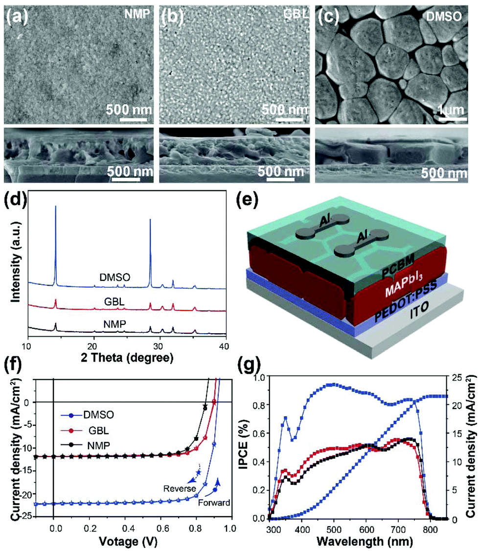 | ||
| Fig. 2 Structural characterization and photovoltaic applications of MAPbI3 films. (a–c) Top and cross-sectional SEM images of the perovskite films engineered with NMP, GBL, and DMSO as indicated. (d) The corresponding XRD patterns of these perovskite films. (e) Schematic of a perovskite solar cell. (f) The corresponding J–V curves of solar cells fabricated from these MAPbI3films. (g) The corresponding IPCE spectra of the devices. | ||
Photovoltaic devices were then fabricated using these MAPbI3 films, as schematically shown in Fig. 2e. The photovoltaic device based on the D-perovskite film exhibited the best photovoltaic performance with a power conversion efficiency of 17.51%. The corresponding incident photon to current efficiency (IPCE) spectra are shown in Fig. 2f and g. The detailed parameters of the perovskite solar cells are summarized in Table 1. From these results, we conclude that strong interactions between a Lewis base solvent and Pb2+ in the precursor solution suppresses MAPbI3 nucleation and decreases the density of nuclei in the film, resulting in highly crystalline grains with enlarged size. This leads to improvements in the perovskite film quality and its photoelectric properties.
| Device | J SC (mA cm−2) | V OC (V) | FF (%) | PCE (%) |
|---|---|---|---|---|
| G-Perovskite | 11.87 | 0.90 | 0.78 | 8.33 |
| N-Perovskite | 11.76 | 0.85 | 0.76 | 7.75 |
| D-Perovskite | 22.09 | 0.95 | 0.83 | 17.51 |
Growth mechanism of crystalline MAPbI3 nanostructures
Because the Lewis base solvents are usually mixed with DMF in the conventional film fabrication process, the effect of the concentration of DMSO in the mixed solvent of DMSO and DMF on MAPbI3 nucleation was investigated. Fig. 3a–d show the morphology variation of the precursor films with increasing DMSO concentration in the mixed solvent. The final morphologies of complete perovskite films after annealing are shown at the bottom. When the DMSO content was increased, the typical rod-like morphology of the intermediate phase persisted (Fig. 3c) and porous tube aggregates were observed. However, excess DMSO in the mixed solvent led to the formation of obvious holes in the films due to the fast crystallization of the perovskite (Fig. 3d) via re-dissolution of PbI2 by the excess DMSO. These features persist into the final morphologies of the complete perovskite films after annealing. In the annealing process, we employed the merged annealing (MA) method to delay the evolution of the morphology by retarding the solvent evaporation speed using shielding materials.31 As expected, the grain size of the final perovskite film increased with increasing DMSO content. However, excess DMSO in the mixed solvent indeed leads to a low quality perovskite film with obvious holes in the film. It can be concluded that the nucleation and growth of the perovskite crystal following a passivated nucleation process with a Lewis base solvent results in a larger grain size but the amount of Lewis base solvent must be optimized. A similar crystallization trend was also observed in perovskite films prepared by a conventional annealing (CA) method as shown in Fig. S2.†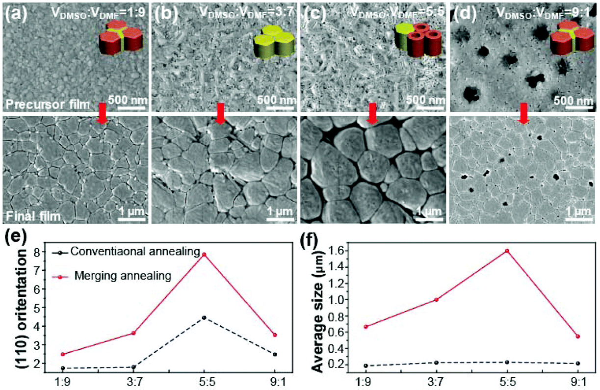 | ||
| Fig. 3 Morphology and structural properties of as-deposited and DMSO modulated perovskite films. Top-view SEM images of (a–d) precursor films mediated by DMSO/DMF system and their corresponding perovskite films. (e) Plot of orientation of (110) planes and (f) average grain size of the perovskite films with different annealing strategy. ImageJ was used to measure the grain size of the perovskite films. | ||
XRD patterns of the precursor films prepared with different solvent ratios of DMSO and DMF before annealing are shown in Fig. S3.† All precursor films exhibited the typical XRD peaks of a perovskite precursor with noticeable peaks at 9.2° and 14.12°. The peaks at 9.2° and 14.12° were assigned to the (022) facet of the intermediate phase and the (110) facet of the complete MAPbI3 perovskite, respectively. Therefore, the peak at 14.12° became predominant after annealing, whereas the intermediate peak at 9.2° disappeared after the complete perovskite film was formed (see the XRD of the complete film in Fig. S4†). As shown in Fig. S5,† the diffraction intensity of the intermediate peak decreases with increased NMP and GBL ratios in the mixed solvent.
One interesting result can be obtained from the comparison of the (110) peak intensity and the corresponding grain sizes of the films fabricated by the MA and CA methods. The grain sizes of the perovskite films were extracted from the SEM images shown in Fig. 3 and S2† using the ImageJ program. Fig. 3e and f show the variation in the (110) facet intensity and corresponding grain size, respectively, for different solvent mixing ratios of solvents. As expected, the highest (110) peak intensity and largest grain size were obtained in the MA film with a 5![[thin space (1/6-em)]](https://www.rsc.org/images/entities/char_2009.gif) :5 ratio. This indicates that the large grains are highly crystalline and oriented in the (110) direction. However, this tendency was not observed in the CA film (see the black-dotted line in Fig. 3f). While a high (110) peak intensity was also observed for the CA film with a 5:5 ratio, the grain size of the film was comparable to those of films with ratios of 1:9 and 3:7. These results imply that the preferred crystal facet and grain size are independent of each other, which will be used to study the key factors affecting film stability under humidity.
:5 ratio. This indicates that the large grains are highly crystalline and oriented in the (110) direction. However, this tendency was not observed in the CA film (see the black-dotted line in Fig. 3f). While a high (110) peak intensity was also observed for the CA film with a 5:5 ratio, the grain size of the film was comparable to those of films with ratios of 1:9 and 3:7. These results imply that the preferred crystal facet and grain size are independent of each other, which will be used to study the key factors affecting film stability under humidity.
The underlying mechanisms that control the film growth process are a subject for further discussion. To reveal the details of the growth process, we studied the composition and morphology evolution of the perovskite film during annealing by a series of XRD and SEM measurements, as shown in Fig. 4. The evolution of the crystal structure of the non-annealed film was revealed by XRD analysis, as shown in Fig. 4a. Initially, the precursor film showed a low degree of crystallinity with broad, low intensity diffraction peaks centered at low diffraction angles of 7.0° and 9.2°, which correspond to the (020) and (022) planes of intermediate phases. After prolonged annealing, the intensity ratio of the (020) and (022) peaks was enhanced, indicating the (010)-oriented growth of the intermediate phase in the film. The oriented grain growth of the intermediate continues for the first 120 s of the annealing process, as revealed by the increased intensity of the (020) peak. After that, the perovskite phase starts its oriented growth, as revealed by the enhanced intensity of the (110) peak and the peak ratio of (110) to (310). The (020) plane of the intermediate and the (110) plane of the perovskite in the unit crystal structure are briefly described in the light part of the XRD spectrum.
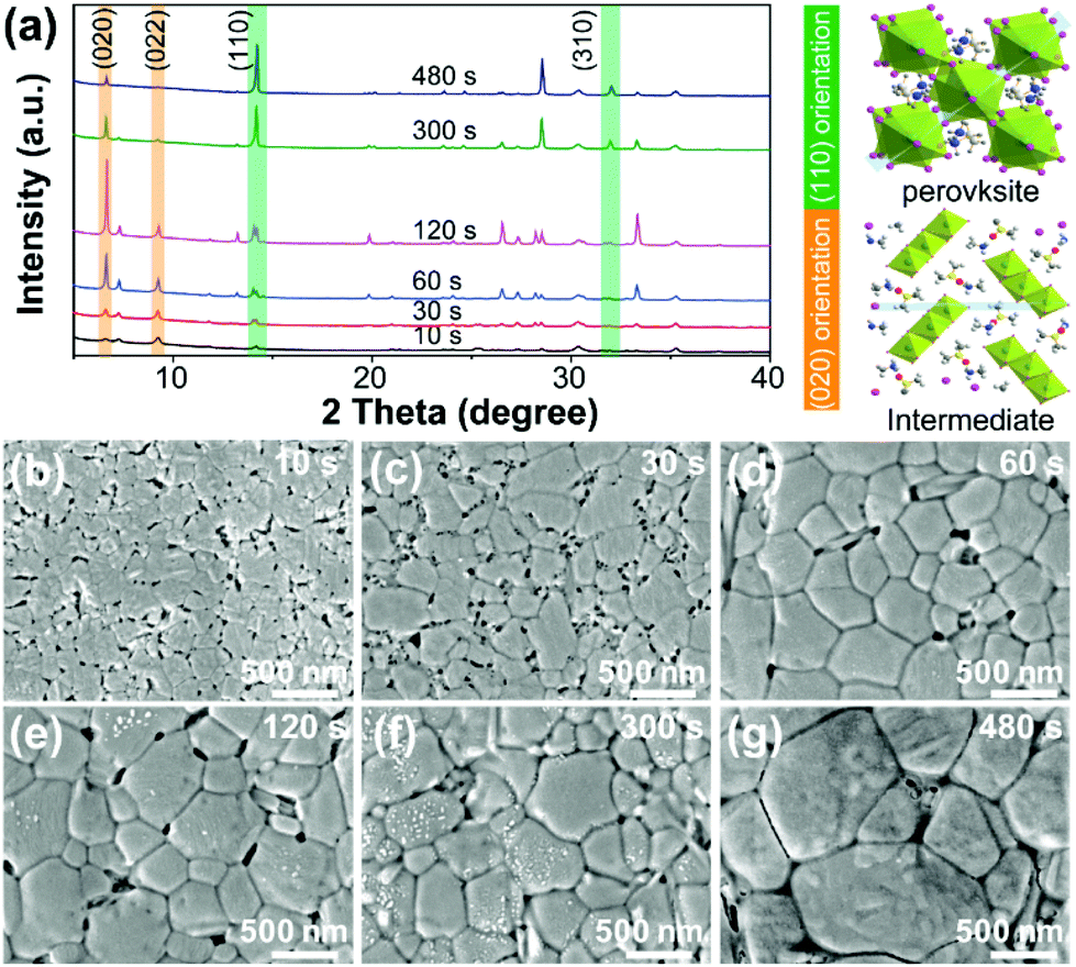 | ||
| Fig. 4 Growth process of perovskite films. (a) XRD patterns showing evolution of film structures with annealing. The orange rectangle indicates the (020)-oriented growth of (MAI)2Pb3I8·2DMSO. The green rectangle demonstrates the (110)-oriented growth of MAPbI3. Right panel: Unit crystal structures of (MAI)2Pb3I8·2DMSO and MAPbI3 crystals, respectively. The light blue areas show the (020) and (110) planes of (MAI)2Pb3I8·2DMSO and MAPbI3, respectively. (b–g) Top-view SEM images of the as-grown MAPbI3 films at different annealing times of (b) 10 s, (c) 30 s, (d) 60 s, (e) 180 s, (f) 300 s, and (g) 480 s, respectively. | ||
Time-dependent SEM images were used to demonstrate the morphology evolution during the crystallization process, as shown in Fig. 4b–g. When the annealing time increased to 10 s, a columnar species could be observed and compared with the morphology of the film shown in Fig. 3c. The newly formed species showed a relative contrast compared to the adjacent tubular aggregates. Based on the XRD analysis, we assume that these columnar grains belong to another state of the intermediate phase with numerous holes located in the grain boundary zones, which we regard as the tubular perovskite phase. Additionally, when the annealing time increased to 120 s, the grains become larger with the help of recycled DMSO vapor using the MA method, and the pinhole density at the grain boundary decreased. Finally, the obtained perovskite film was compact and conformal.
Based on the above discussion, the overall crystallization process of perovskite grains consists of three steps (i.e., nucleation, (020)-oriented intermediate growth, and (110)-oriented perovskite growth), as shown in Fig. 5. During the nucleation process (stage (i)), a moderate amount of DMSO molecules induce the formation of the predominant intermediate phase with a small amount of the perovskite phase.33 A sparse number of perovskite nuclei can effectively serve as nucleation sites for newly formed perovskite crystals transformed from the intermediate state. If a large number of perovskite nuclei are present in the as-deposited film, they will grow directly upon heating, leading to faster crystallization kinetics than in the case of an as-deposited film with more of the intermediate phase. Moreover, our earlier work has demonstrated that the MA method can slow down the evaporation of solvent molecules in ambient atmosphere.31 Thus, in the initial annealing process (stage (ii)), the oriented growth of the intermediate phase occurs by use of recycled DMSO vapor. Finally, the active species from the decomposed intermediate phase migrate to the interface or surface of the perovskite, leading to the enlargement of the perovskite grains (stages (iii) and (iv)).
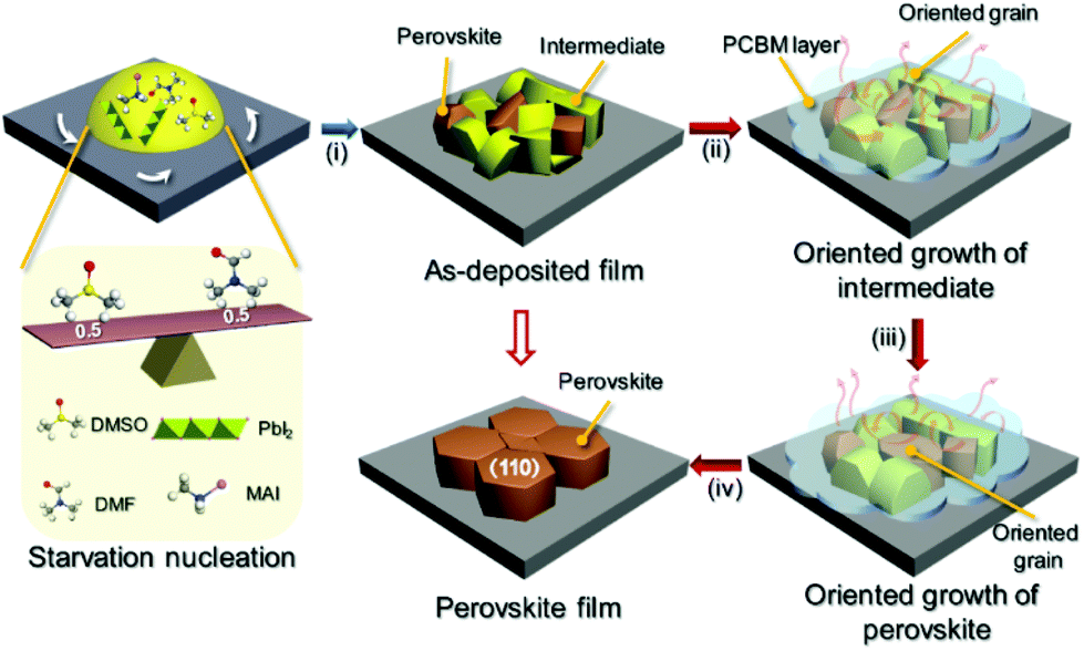 | ||
| Fig. 5 Schematics of perovskite grain growth. Stage i shows the nucleation process. Stage ii shows the oriented growth of intermediate crystals. Stages iii and iv demonstrate the oriented growth of perovskite crystals. | ||
Critical factors determining the structural stability of perovskite films
Since previous works have shown that perovskite films with larger grain sizes mostly exhibited a higher degree of orientation in the (110) direction, it was believed that there was strong correlation between grain size and orientation.34,35 Therefore, no comparative study of the effects of (110) crystal facet and grain size on the structural stability of perovskite film has yet been performed. In this work, however, we found that the crystal facet and grain size are independent of each other and thus we investigated the effect of these two factors on the moisture stability of perovskites. Fig. 6a depicts three kinds of perovskite active layers with different grain structures and the corresponding perovskite films are described in Fig. S2c,†Fig. 3b and 3c. The films exhibited three different morphologies: (i) small but highly oriented grains, (ii) large, mostly un-oriented grains, and (iii) large and highly oriented grains, respectively.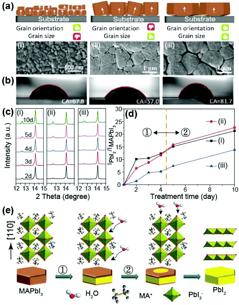 | ||
| Fig. 6 Key factors influencing the moisture stability of perovskite film. (a) The schematics of three types perovskite grains, and the respective (b) contact angle between perovskite films and a water droplet. (i) Perovskite grains with high grain orientation and small grain size; (ii) perovskite grains with small grain orientation and large grain size; (iii) perovskite grains with high grain orientation and large grain size. (c) XRD patterns showing the evolution of the three perovskite grain types under ambient conditions (30 °C, 45–60% humidity). (d) The degradation percentage of the perovskite films with increasing treatment time. (e) Illustration of the two-step degradation process. (①) is the grain boundary degradation resulting from the abundant defects. (②) is the grain surface degradation. | ||
The contact angles of deionized water droplets on the perovskite films are shown in Fig. 6b. Film (i) exhibited a lower contact angle of 67.8°, which is lower than the angle of 81.7° measured for film (iii), but higher than the angle of 57.0° measured for film (ii). Because the more highly oriented films exhibited higher contact angles, we expect that the degree of facet orientation affects the surface properties more than grain size does.36 A higher water contact angle implies higher water resistance. Therefore, it is obvious that the (110) orientation of the surface leads to a more hydrophobic perovskite film and consequently, enhanced moisture stability. In order to verify this conclusion, we investigated variations in the XRD peaks at 12.6° and 14.12°, which correspond to PbI2 and MAPbI3, respectively, under prolonged exposure to air with a humidity of 45–60%. Fig. 6c and 6d exhibit the evolution of the (110) peak of complete MAPbI3 at 14.12° and the peak ratio of PbI2 to MAPbI3 under increasing exposure times. In addition, Fig. S6† shows the photographs of perovskite films with increasing exposure time. Because the MAPbI3 easily decompose to MAI and PbI2 with moisture, their ratio indicates the degree of degradation by moisture.37 As shown in Fig. 6d, film (iii) exhibited the best moisture stability, whereas films (i) and (ii) showed comparable stability to each other. This tendency is also observed in stability results of the typical devices in Fig. S7.† This indicates that a higher degree of (110) orientation and larger grain size improve the moisture stability of the perovskite film. However, the degradation of a perovskite grain consists of two stages, labeled stage ① and ② in Fig. 6d. In stage ①, the degradation rate is proportional to the grain size. Since the grain boundaries have a more amorphous state and defective regions compared to the crystalline region, moisture can permeate more easily along the grain boundary.38 However, after four days of exposure (stage ②), the (110) facet became a dominant factor determining the moisture stability, confirmed by the cross point between the black and red lines in Fig. 6d. Under prolonged moisture exposure, the MAPbI3 first decomposes to MAI and PbI2 with moisture at the grain boundaries, corresponding to stage ①.39 The newly formed PbI2 at the grain boundaries is more hydrophobic than MAPbI3 at grain surfaces. Thus, after process ① finishes, the degradation of perovskite grains begins again at the grain surface due to the decreased hydrophobicity. Schematic illustration of the degradation process of a perovskite grain is displayed in Fig. 6e.
Conclusions
In summary, we investigated the growth mechanism of MAPbI3 perovskite films and the governing factors which determine the morphological properties of the final perovskite crystal such as grain size and crystal facet orientation. Using different Lewis base solvents, which have different electron densities around their oxygen atoms, and different annealing times, we modulated the grain size and (110) facet orientation of MAPbI3 perovskite films. A single layer of micrometer-sized and (110)-oriented perovskite crystals in the optimized MAPbI3 films was successfully assembled via suppressing the nucleation rate. Traces of perovskite phase in the precursor film act as nucleation sites for the growth of perovskite crystals and therefore, suppressing the generation of nucleation sites results in a highly crystalline perovskite film with enlarged grain sizes and (110) facet orientation, leading to remarkable enhancement in solar cell efficiency. A PCE of 17.5% in IPSC was achieved by this method without displaying any distinct hysteresis. Furthermore, we conducted the first comparative study of the effects of (110) crystal facet orientation and grain size on the structural stability of perovskite films, and found that the crystal orientation and grain size are independent factors determining the surface properties and moisture stability of the perovskite film. The (110) facet orientation of the perovskite grains plays a more important role in film degradation than grain size.Conflicts of interest
There are no conflicts to declare.Acknowledgements
This research was mainly supported by the Global Frontier Program through the Global Frontier Hybrid Interface Materials (GFHIM) of the National Research Foundation of Korea (NRF) funded by the Ministry of Science, ICT & Future Planning (2013M3A6 B1078874). This research was also supported by the NRF Grant funded by the Korea Government (NRF-2016R1A2B4011474).Notes and references
- H. Tsai, R. Asadpour, J.-C. Blancon, C. C. Stoumpos, O. Durand, J. W. Strzalka, B. Chen, R. Verduzco, P. M. Ajayan, S. Tretiak, J. Even, M. A. Alam, M. G. Kanatzidis, W. Nie and A. D. Mohite, Science, 2018, 360, 67 CrossRef CAS PubMed.
- Y. Deng, X. Zheng, Y. Bai, Q. Wang, J. Zhao and J. Huang, Nat. Energy, 2018, 3, 560 CrossRef CAS.
- P. Wang, X. Zhang, Y. Zhou, Q. Jiang, Q. Ye, Z. Chu, X. Li, X. Yang, Z. Yin and J. You, Nat. Commun., 2018, 9, 2225 CrossRef PubMed.
- J.-W. Lee, Z. Dai, C. Lee, H. M. Lee, T.-H. Han, N. De Marco, O. Lin, C. S. Choi, B. Dunn, J. Koh, D. Di Carlo, J. H. Ko, H. D. Maynard and Y. Yang, J. Am. Chem. Soc., 2018, 140, 6317 CrossRef CAS PubMed.
- S. R. Ha, S. Park, J. T. Oh, D. H. Kim, S. Cho, S. Y. Bae, D.-W. Kang, J.-M. Kim and H. Choi, Nanoscale, 2018, 10, 13187 RSC.
- S. Y. Leblebici, L. Leppert, Y. Li, S. E. Reyes-Lillo, S. Wickenburg, E. Wong, J. Lee, M. Melli, D. Ziegler, D. K. Angell, D. F. Ogletree, P. D. Ashby, F. M. Toma, J. B. Neaton, I. D. Sharp and A. Weber-Bargioni, Nat. Energy, 2016, 1, 16093 CrossRef CAS.
- J. Yin, D. Cortecchia, A. Krishna, S. Chen, N. Mathews, A. C. Grimsdale and C. Soci, J. Phys. Chem. Lett., 2015, 6, 1396 CrossRef CAS PubMed.
- D. W. deQuilettes, S. M. Vorpahl, S. D. Stranks, H. Nagaoka, G. E. Eperon, M. E. Ziffer, H. J. Snaith and D. S. Ginger, Science, 2015, 348, 683 CrossRef CAS PubMed.
- W. Tress, N. Marinova, O. Inganas, M. K. Nazeeruddin, S. M. Zakeeruddin and M. Graetzel, Adv. Energy Mater., 2015, 5, 1400812 CrossRef.
- F. Xie, C.-C. Chen, Y. Wu, X. Li, M. Cai, X. Liu, X. Yang and L. Han, Energy Environ. Sci., 2017, 10, 1942 RSC.
- Z. Zuo, J. Ding, Y. Zhao, S. Du, Y. Li, X. Zhan and H. Cui, J. Phys. Chem. Lett., 2017, 8, 684 CrossRef CAS PubMed.
- H. Zhang, X. Ren, X. Chen, J. Mao, J. Cheng, Y. Zhao, Y. Liu, J. Milic, W.-J. Yin, M. Grätzel and W. C. H. Choy, Energy Environ. Sci., 2018, 11, 2253 RSC.
- H. Lei, X. Chen, L. Xue, L. Sun, J. Chen, Z. Tan, Z.-G. Zhang, Y. Li and G. Fang, Nanoscale, 2018, 10, 8088 RSC.
- J. Feng, X. Zhu, Z. Yang, X. Zhang, J. Niu, Z. Wang, S. Zuo, S. Priya, S. Liu and D. Yang, Adv. Mater., 2018, 30, 1801418 CrossRef PubMed.
- Z. Wu, S. R. Raga, E. J. Juarez-Perez, X. Yao, Y. Jiang, L. K. Ono, Z. Ning, H. Tian and Y. Qi, Adv. Mater., 2018, 30, 1703670 CrossRef PubMed.
- B. Zhang, M.-J. Zhang, S.-P. Pang, C.-S. Huang, Z.-M. Zhou, D. Wang, N. Wang and G.-L. Cui, Adv. Mater. Interfaces, 2016, 3, 1600327 CrossRef.
- W. Kim, M. S. Jung, S. Lee, Y. J. Choi, J. K. Kim, S. U. Chai, W. Kim, D.-G. Choi, H. Ahn, J. H. Cho, D. Choi, H. Shin, D. Kim and J. H. Park, Adv. Energy Mater., 2018, 8, 1702369 CrossRef.
- Y. Ma, J. Lee, Y. Liu, P. M. Hangoma, W. I. Park, J.-H. Lim, Y. K. Jung, J. H. Jeong, S. H. Park and K. Kim, Nanoscale, 2018, 10, 9628 RSC.
- Y. Zhou, O. S. Game, S. Pang and N. P. Padture, J. Phys. Chem. Lett., 2015, 6, 4827 CrossRef CAS PubMed.
- Y. Zhao, H. Tan, H. Yuan, Z. Yang, J. Z. Fan, J. Kim, O. Voznyy, X. Gong, L. N. Quan, C. S. Tan, J. Hofkens, D. Yu, Q. Zhao and E. H. Sargent, Nat. Commun., 2018, 9, 1607 CrossRef PubMed.
- M. Xiao, L. Zhao, M. Geng, Y. Li, B. Dong, Z. Xu, L. Wan, W. Li and S. Wang, Nanoscale, 2018, 10, 12141 RSC.
- H. Dong, Z. Wu, J. Xi, X. Xu, L. Zuo, T. Lei, X. Zhao, L. Zhang, X. Hou and A. K.-Y. Jen, Adv. Funct. Mater., 2018, 28, 1704836 CrossRef.
- K. Meng, L. Wu, Z. Liu, X. Wang, Q. Xu, Y. Hu, S. He, X. Li, T. Li and G. Chen, Adv. Mater., 2018, 30, 1706401 CrossRef PubMed.
- R. Munir, A. D. Sheikh, M. Abdelsamie, H. Hu, L. Yu, K. Zhao, T. Kim, O. E. Tall, R. Li, D.-M. Smilgies and A. Amassian, Adv. Mater., 2017, 29, 1604113 CrossRef PubMed.
- P. Sonar, G.-M. Ng, T. T. Lin, A. Dodabalapur and Z.-K. Chen, J. Mater. Chem., 2010, 20, 3626 RSC.
- H. Wang, P. Zhang, P. Zhou, R. Xu and Y. Tang, RSC Adv., 2018, 8, 18406 RSC.
- Z. Liu, J. Hu, H. Jiao, L. Li, G. Zheng, Y. Chen, Y. Huang, Q. Zhang, C. Shen, Q. Chen and H. Zhou, Adv. Mater., 2017, 29, 1606774 CrossRef PubMed.
- K. Yan, M. Long, T. Zhang, Z. Wei, H. Chen, S. Yang and J. Xu, J. Am. Chem. Soc., 2015, 137, 4460 CrossRef CAS PubMed.
- Y. Jo, K. S. Oh, M. Kim, K.-H. Kim, H. Lee, C.-W. Lee and D. S. Kim, Adv. Mater. Interfaces, 2016, 3, 1500768 CrossRef.
- J. Cao, X. Jing, J. Yan, C. Hu, R. Chen, J. Yin, J. Li and N. Zheng, J. Am. Chem. Soc., 2016, 138, 9919 CrossRef CAS PubMed.
- Y. Liu, I. Shin, I.-W. Hwang, S. Kim, J. Lee, M.-S. Yang, Y. K. Jung, J.-W. Jang, J. H. Jeong, S. H. Park and K. H. Kim, ACS Appl. Mater. Interfaces, 2017, 9, 12382 CrossRef CAS PubMed.
- F. X. Xie, D. Zhang, H. Su, X. Ren, K. S. Wong, M. Grätzel and W. C. H. Choy, ACS Nano, 2015, 9, 639 CrossRef CAS PubMed.
- L. Zuo, S. Dong, N. De Marco, Y.-T. Hsieh, S.-H. Bae, P. Sun and Y. Yang, J. Am. Chem. Soc., 2016, 138, 15710 CrossRef CAS.
- W. Zhu, L. Kang, T. Yu, B. Lv, Y. Wang, X. Chen, X. Wang, Y. Zhou and Z. Zou, ACS Appl. Mater. Interfaces, 2017, 9, 6104 CrossRef CAS PubMed.
- G. Xu, R. Xue, W. Chen, J. Zhang, M. Zhang, H. Chen, C. Cui, H. Li, Y. Li and Y. Li, Adv. Energy Mater., 2018, 8, 1703054 CrossRef.
- Y. Chang, L. Wang, J. Zhang, Z. Zhou, C. Li, B. Chen, L. Etgar, G. Cui and S. Pang, J. Mater. Chem. A, 2017, 5, 4803 RSC.
- M. Long, T. Zhang, Y. Chai, C.-F. Ng, T. C. W. Mak, J. Xu and K. Yan, Nat. Commun., 2016, 7, 13503 CrossRef CAS PubMed.
- Q. Wang, B. Chen, Y. Liu, Y. Deng, Y. Bai, Q. Dong and J. Huang, Energy Environ. Sci., 2017, 10, 516 RSC.
- Q. Chen, H. Zhou, T.-B. Song, S. Luo, Z. Hong, H.-S. Duan, L. Dou, Y. Liu and Y. Yang, Nano Lett., 2014, 14, 4158 CrossRef CAS PubMed.
Footnote |
| † Electronic supplementary information (ESI) available. See DOI: 10.1039/c8nr08344d |
| This journal is © The Royal Society of Chemistry 2019 |