DOI:
10.1039/C8NR07353H
(Paper)
Nanoscale, 2019,
11, 158-169
From one-dimensional to two-dimensional wurtzite CuGaS2 nanocrystals: non-injection synthesis and photocatalytic evolution†
Received
10th September 2018
, Accepted 11th November 2018
First published on 12th November 2018
Abstract
Multinary copper-based chalcogenides exhibit significant performance in photocatalytic hydrogen evolution due to their suitable optical bandgap for visible light absorption and environmentally friendly character. Herein, high-quality wurtzite CuGaS2 (CGS) nanocrystals (NCs) were synthesized by using a one-step heating-up process without any injection, and the morphology could be tuned from one-dimensional (1D) to two-dimensional (2D) by precise choice of surface ligands and gallium precursors. The formation mechanism of CGS NCs was studied comprehensively by means of the temporal-evolution of the morphology, crystal structure and optical absorption results. The reaction started from djurleite Cu31S16 NCs, and then proceeded with the formation of Cu31S16–CGS heteronanostructures (HNS), and finally the transformation from HNS to monophasic CGS nanorods took place with prolonging of the synthesis time. The optical bandgap and the energy level of the different-dimensional CGS NCs exhibited a strong dependence on the morphology change, which correlated with the percentage of the exposed {001} and {100} facets. The theoretical calculation based on density functional theory (DFT) revealed that the (001) surface facilitated the charge transport rather than the (100) surface, which was consistent with the electrochemical impedance spectroscopy (EIS) results. As a result, the 2D CGS nanoplates with more exposed {001} facets exhibited an attractive photocatalytic hydrogen production activity under simulated solar illumination as compared to 1D and quasi-2D counterparts. This study demonstrates that control over the dimension of I–III–V group semiconductor NCs could lead to a significant improvement of the photocatalytic hydrogen evolution.
1. Introduction
Cadmium (Cd-) and lead (Pb-)-based semiconductor NCs have been widely studied over the past few decades, and they showed attractive applications in light-emitting diodes, solar cells, photocatalysis and photo-detectors.1–8 Unfortunately, heavy elements, such as Cd and Pb, have restricted further applications due to their higher toxicity and environmental pollution. Therefore, it is of great interest to search for environmentally benign alternative nanomaterials to replace Cd- and Pb-based semiconductor NCs. Among different types of potentially alternative materials, ternary and quaternary Cu-based chalcogenide compounds including CuInS2 and Cu–In–Zn–S NCs have become one of the hot research topics in the past several years, and they exhibit promising applications in optoelectronic devices and photocatalysis.9–17 In particular, CuInS2 is a direct semiconductor with a band gap of 1.45 eV and a high absorption coefficient, matching well with the solar spectrum.9,10 As a result, substantial progress has been made in the synthesis of CuInS2 NCs and their applications in light-emitting diodes, solar energy conversion and photocatalysis.13–20 Both the Cui and Kolny-Olesiak groups stated in their respective report that the formation started with the nucleation of Cu2S NCs, followed by the formation of Cu2S–CuInS2 HNS, which was an essential intermediate step in the growth of CuInS2 NCs.21,22 These studies provided a valuable insight into the controllable synthesis of I–III–VI chalcogenide NCs.
As another important member of the ternary Cu-based chalcogenide family, CGS has a band gap of 2.4 eV, which can be used as an ideal host material in intermediate-band solar cells.23–25 Moreover, CGS is also widely used in light-emitting devices and solar-light-induced photocatalysis.26–29 Therefore, the synthesis of ternary CGS NCs has attracted much attention in recent years. Although different-shaped CGS NCs with a chalcopyrite structure have been synthesized through a solvothermal or hydrothermal technique, the as-obtained products are mostly polydisperse and appear in the form of large crystals.30–32 Since Wang et al. reported the synthesis of wurtzite CGS NCs by using a hot-injection strategy,23 different solution-based methods have been developed to prepare CGS NCs.33–39 For example, Xiao et al. reported a facile and reliable one-pot approach to prepare metastable wurtzite CGS NCs, and they demonstrated that the pressure played a significant role in the phase transformation.35 Chang et al. synthesized different-shaped chalcopyrite and wurtzite CGS NCs by varying the sulfur sources and the amount of the organic ligands.38 In these reports, however, the morphology control was overemphasized but the formation mechanism of CGS NCs was overlooked. As a result, it is necessary to study the formation mechanism of wurtzite CGS NCs and precisely control the dimensions of CGS NCs.
With an increase in demand on the photocatalytic hydrogen production under visible light, much attention was turned from micro- or nano-sized TiO2 to narrow-bandgap metal chalcogenide NCs.40–44 Very recently, ternary or quaternary Cu-based chalcogenide NCs have been developed and widely used in the photocatalytic hydrogen production, and the performance is competitive with that of the state-of-the-art II–VI group semiconductor NCs.43,44 However, the study on the photocatalytic hydrogen evolution of Cu-based chalcogenide NCs is just in the infancy stage, and there is no end to explore the relationship between the photocatalytic performance and the intrinsic properties of Cu-based chalcogenide NCs. Until now, most of the reports have mainly focused on the composition-tunable photocatalytic activity,16,29,44 and the effects of the different exposed facets on the photocatalytic performance are rarely reported. In this work, a one-pot colloidal approach was developed to prepare different-dimensional CGS NCs with a wurtzite crystal structure. The percentage of the {001} and {100} facets in different-dimensional CGS NCs could be engineered by the choice of surface ligands and gallium precursors, resulting in the formation of 1D nanorods, quasi-2D nanodisks and 2D nanoplates. The formation of 1D CGS nanorods started with the nucleation of djurleite Cu31S16 nanospheres, followed by the formation of Cu31S16–CGS HNS due to the partial cation inter-diffusion process, which finally led to the transformation from Cu31S16–CGS HNS into monophasic CGS nanorods with the growth proceeding. The optical bandgap, energy level and charge transport of different-dimensional CGS NCs exhibited a strong morphology-dependent behavior, which could be confirmed by the theoretical and experimental results. The photocatalytic activity of the 1D, quasi-2D and 2D CGS NCs was measured for the evolution of hydrogen in the presence of Na2S and Na2SO3 as hole scavengers, and the 2D CGS nanoplates exhibited a better photocatalytic performance since the (001) surface offered more photo-generated electrons and facilitated the charge transport.
2. Experimental section
2.1 Materials
Copper(II) acetylacetonate (Cu(acac)2, 97%), gallium(III) acetylacetonate (Ga(acac)3, 97%), gallium(III) chloride (GaCl3, 99.99%), sodium sulfite (Na2SO3, 98%), sodium sulfide nonahydrate (Na2S·9H2O, 99.99%), 3-mercaptopropionic acid (MPA, 98%), oleylamine (OM, >80%) and 1-dodecanethiol (DDT, 98%) were purchased from Shanghai Aladdin Reagent Company. 1-Octadecene (ODE, 90%) and tetra-n-butylammonium hexafluorophosphate (98%) were purchased from Alfa. Formamide was purchased from Sinopharm Chemical Reagent Co. Ltd (Shanghai, China) and other solvents such as ethanol, chloroform and acetonitrile were commercially available products of analytical grade, which were purchased from Beijing Chemical Reagent, China. All of the chemicals were used as received without further purification.
2.2 Synthesis of 1D CGS nanorods
The synthesis of 1D CGS nanorods was based on the following procedures: 2.5 mmol Cu(acac)2 and 2.5 mmol Ga(acac)3 were mixed with 5 mL of DDT and 25 mL of ODE in a three-necked flask, and the mixture was degassed under a N2 flow for 10 min at room temperature with magnetic stirring. Then the temperature was elevated to 140 °C and maintained for 30 min to eliminate adventitious water and dissolved oxygen. Afterwards, the reaction mixture was heated slowly to 240 °C under a N2 atmosphere and maintained for 60 min. Subsequently, the reaction mixture was cooled to room temperature naturally and the as-obtained products were purified by four repeated actions of dissolving the precipitate in chloroform and then re-precipitating by addition of excess ethanol. Finally, the resultant samples were re-dispersed in chloroform solvent or dried under vacuum for further characterization. To study the formation mechanism of CGS nanorods, different samples were synthesized by varying the reaction temperature (200 °C, 220 °C and 250 °C) and the reaction time from 0 to 60 min, while other reaction conditions were kept the same as described above.
2.3 Synthesis of quasi-2D CGS nanodisks
The synthesis of quasi-2D CGS nanodisks was similar to the synthetic procedure of 1D CGS nanorods. Typically, 2.5 mmol Cu(acac)2 and 2.5 mmol Ga(acac)3 were mixed with 5 mL of DDT and 20 mL of ODE in a three-necked flask, and an additional 5 ml of OM as a co-ligand were added into the three-necked flask. In addition, the other reaction conditions, the washing and precipitation process, were unchanged. Herein, the reaction temperature was set at 220 °C and 240 °C.
2.4 Synthesis of 2D CGS nanoplates
The synthesis of 2D wurtzite CGS nanoplates was performed according to the synthetic procedure of 1D CGS nanorods except that Ga(acac)3 was changed to GaCl3, and the other reaction conditions including the washing and precipitation process were unchanged. Herein, the reaction temperature was fixed at 220 °C and 240 °C.
2.5 Synthesis of CGS with different Cu/Ga molar ratios
The seed-mediated growth approach was used to synthesize CGS NCs with different amounts of Ga precursors. Typically, djurleite Cu31S16 nanopheres were synthesized based on our previous work.45 Subsequently, a Ga precursor solution containing 5 mL of DDT, 5 mL of ODE and a certain content of Ga(acac)3 was injected into Cu31S16 NC seeds and then the reaction mixture was kept at 200 °C for several hours. In addition, the other reaction conditions including the washing and precipitation process were kept the same as that mentioned above. Herein, the molar ratios of Cu/Ga precursors were kept at 1![[thin space (1/6-em)]](https://www.rsc.org/images/entities/char_2009.gif) :1 and 1:5, respectively.
:1 and 1:5, respectively.
2.6 Synthesis of CGS with different DDT dosages
The synthesis of CGS NCs with different DDT dosages was similar to the synthetic procedures of 1D CGS nanorods. Typically, 2.5 mmol Cu(acac)2 and 2.5 mmol Ga(acac)3 were mixed with DDT and ODE, whose total volume was kept at 30 mL. In addition, the other reaction conditions were kept unchanged. Herein, the DDT dosage was 1 mL, 2 mL, 5 mL and 30 mL, and the reaction temperature was set at 200 °C and 250 °C.
2.7 Characterization
Transmission electron microscopy (TEM) images were recorded on a JEM-1400 transmission electron microscope with an acceleration voltage of 100 kV. High-resolution TEM images were recorded on a JEM-2010 with an acceleration voltage of 200 kV. X-ray diffraction (XRD) patterns were recorded on a Bruker D8 Advance diffractometer using a Cu Kα radiation source (λ = 1.54056 Å). The simulated XRD pattern of wurtzite CGS NCs was obtained by using TOPAS software and the modes of crystal structures were displayed by the Diamond 3.2 software. X-ray photoelectron spectroscopy (XPS) measurements were carried out by using a VG ESCALAB220i-XL spectrometer with a 300 W Al Kα radiation source. All binding energies for the different elements were calibrated with respect to the C 1s line at 284.8 eV from the contaminant carbon. Ultraviolet photoemission spectroscopy (UPS) data were obtained with an Axis Ultra DLD multi-technique spectrometer. Electrochemical impedance spectroscopy (EIS) measurements were carried out on a CHI 660D electrochemical workstation. The Fourier transform infrared (FTIR) spectrum was recorded by using a Varian Excalibur 3100 spectrometer. The ultraviolet-visible absorption spectra were collected by using an HR2000CG-UV-NIR spectrometer from Ocean Optics. The diffuse reflectance spectra (DRS) were obtained using a Varian 5000 spectrophotometer equipped with an integrating sphere using BaSO4 as a reference. All of the measurements were performed at room temperature.
2.8 Photocatalytic activity measurement
Before the evaluation of photocatalytic activity, three samples including 1D, quasi-2D and 2D CGS NCs should be firstly transferred from nonaqueous solvents into the aqueous solution. Typically, the final samples in the chloroform solution were mixed with a formamide solution with MPA (3% volume in solution), which was stirred under vigorous magnetic stirring for 6 h.46 Afterwards, the samples were collected through the centrifugation process, and then the samples were washed and precipitated with acetone and ethanol five times and water three times.
The photocatalytic hydrogen reaction was conducted in an online photocatalytic hydrogen production system (Labsolar-III (AG), Perfectlight, Beijing) equipped with a GC2014 (Shimadzu). Typically, 15 mg of photocatalysts were dispersed in 100 mL of deionized water with a magnetic stirrer, in which 0.1 M Na2S and 0.3 M Na2SO3 were used as hole scavengers. Before irradiation, the reaction system was evacuated to remove the air in the reactor and water. Afterwards, a 500 W Xe lamp was used to simulate the solar light and the average intensity of irradiation was detected by using a radiation meter (Thorlabs, PM100D with S310C). The temperature was maintained at 5 ± 0.2 °C by using a low-constant temperature bath (DC-2006, Shanghai Bilang). The evolved hydrogen was gathered and analyzed by GC (TCD and FID, molecular sieves 5 Å column and Ar carrier).
2.9 DFT calculations
Density functional theory calculations were carried out using the Cambridge Serial Total Energy Package (CASTEP) codes in Materials Studio software, and were based on a plane-wave pseudopotential method.47 The generalized gradient approximation (GGA) of the Perdew–Burke–Ernzerhof functional (PBE) form was employed to optimize the geometry and calculate the electronic structure.48,49 All the calculations were described by the on the fly generated (OTFG) ultrasoft pseudopotential with an energy cutoff of 408.2 eV. The cell structure of CGS with a hexagonal lattice was built from wurtzite-structured ZnS, where Cu and Ga occupied the Zn positions. A Monkhorst–Pack k-point grid of 4 × 4 × 2 was used to sample the Brillouin zone for bulk geometry optimization and electronic structure calculation. The lattice parameters of the optimized cell of CGS were a = 3.852 Å, b = 3.852 Å, and c = 6.298 Å. Different CGS surfaces were structured as repeating slabs of 6 layers separated with a vacuum spacing of 30 Å along the direction perpendicular to the slab surface. The super cell lattice parameters of the (2 × 2) CGS (001) surface and (2 × 2) CGS (100) surface were 7.705 Å × 7.705 Å and 7.705 Å × 12.597 Å, respectively. Two bottom layers in the slab were fixed in the bulk position but the remaining layers were fully relaxed in the simulations. A Monkhorst–Pack k-point mesh, 2 × 2 × 1 for the (001) surface and 2 × 1 × 1 for the (100) surface, was applied to sample the two dimensional Brillouin zone for calculating the CGS (001) surface and CGS (100) surface, respectively. All calculations of geometry optimization could be performed under the convergence criteria for the self-consistent convergence accuracy, and the residual force on each relaxed atom and the maximum displacement were set at 1 × 10⁻⁵ eV per atom, 0.03 eV Å−1 and 0.001 Å, respectively.
3. Results and discussion
3.1 Synthesis and characterization of 1D CGS nanorods
It was stated in previous reports that the choice of surface ligands and metal sources could affect the morphology and crystal phase of ternary Cu-based semiconductor NCs.50–52 Herein, a non-coordinating agent (ODE) was selected as the reaction medium to exclude the effects of the surface ligands on the formation of CGS NCs, and DDT was used as not only a sulfur source but also as a capping agent. Fig. 1 depicts the XRD patterns and TEM images of the products synthesized by directly heating Cu(acac)2 and Ga(acac)3 in a mixture of DDT and ODE at 240 °C. Unexpectedly, the characteristic diffraction peaks of the as-obtained products obtained at 60 min shown in the XRD patterns (Fig. 1a) do not match with the present standard JCPDS card database, which mainly includes the standard XRD patterns of the tetragonal chalcopyrite structure of CuGaS2. Thus, the Rietveld refinement technique is employed to simulate the diffraction patterns of the as-synthesized CGS NCs,53 and the experimental data matched well with the simulated results, which indicates that the XRD patterns of the as-obtained CGS NCs are characteristic of a hexagonal wurtzite structure. The refinement results and cell parameters are given in the ESI.† The corresponding schematic crystal structure of wurtzite CGS is shown in Fig. 1d, which is constructed based on the unit cell of wurtzite ZnS by replacing one Zn atom with 1/2 Ga and 1/2 Cu atoms. A typical TEM image of the corresponding CGS NCs is shown in Fig. 1b, and all the products are 1D nanorods with a uniform size distribution. As shown in Fig. S1,† the as-obtained CGS NCs have a mean length of 12.8 ± 1.6 nm and a width of 4.4 ± 0.6 nm. The selected area electron diffraction pattern (SAED) from lower magnification images was obtained and is shown in the inset of Fig. 1b. The SAED pattern displays one characteristic diffraction ring that can be indexed to the (002) lattice plane of wurtzite CGS. The HRTEM image of an individual CGS nanorod presented in Fig. 1c shows clear lattice fringes with a spacing of 0.307 nm, corresponding to the (002) lattice planes of the bulk wurtzite CGS. Combining the SAED and HRTEM results, the dominant growth direction of 1D CGS nanorods is along the [001] direction. To confirm the valence states and contents of the elements of the as-obtained CGS NCs, X-ray photoelectron spectroscopy (XPS) and energy dispersive spectroscopy (EDS) were performed (Fig. S2 and S3†). The narrow and symmetric feature of Cu 2p peaks is indicative of monovalent Cu, which rules out the presence of Cu(II) due to the absence of the satellite peak (Fig. S2b†).36 The Ga 3d peaks display two peaks at 19.4 and 21.9 eV, and the former one can be attributed to the Ga–S bond, and the latter one may arise from the Ga–O bond (Fig. S2c†).54 The peak in the S 2p region is relatively broad in Fig. S2d,† suggesting that different sulfur species are present in the as-obtained products. The S 2p signal can be fitted into two different doublets, which can be assigned to the sulfide ions and thiolate sulfur bound to the surface (Fig. S2d†).17 The percentage of Cu, Ga, S and C elements is found to be 9.9%, 13.4%, 21.2% and 55.6% from the XPS data, and the EDS results indicate that the content of Cu, Ga, S and C elements is 11.3%, 10.1%, 19.1% and 59.5%, respectively. The Cu/Ga/S atomic ratio from the XPS and EDS data is estimated to be 1.3:1:2.2 and 1.1:1:1.9, respectively. Since the XPS and EDS measurements are often used for surface and bulk analysis of different elements, the difference suggests that more S elements are dispersed on the surface. Moreover, little change is observed in the analysis of C elements, which indicates that the C elements mainly spread over the NC surface.
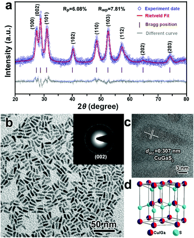 |
| | Fig. 1 (a) Experimental (blue open circles) and simulated (red solid line) XRD patterns, (b) TEM image and (c) a typical HRTEM image of 1D CGS nanorods synthesized at 240 °C for 60 min and the inset is the SAED pattern of the 1D CGS nanorods; (d) schematic model of the crystal structure of wurtzite CGS. | |
3.2 Formation mechanism of CGS NCs
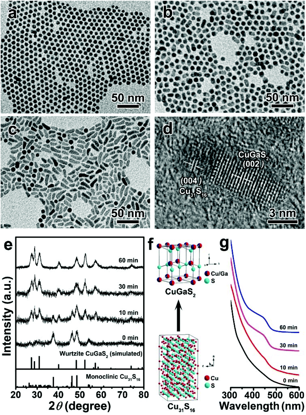
To clarify the formation mechanism of the wurtzite CGS nanorods, the growth process of CGS nanorods obtained at 240 °C for different reaction times was examined. Fig. 2a–c depict the corresponding TEM images of temporal morphology evolution. Initially, uniform nanospheres are obtained at 0 min (Fig. 2a), which can be indexed to monoclinic Cu31S16 based on the XRD patterns shown in Fig. 2e. It is interesting that short matchstick-shaped HNS can be obtained when the reaction time is increased to 10 min (Fig. 2b). The corresponding HRTEM image in Fig. 2d confirms the formation of Cu31S16–CGS HNS, which reveals that the (004) plane of monoclinic Cu31S16 coincides with the (002) plane of wurtzite CGS by careful analysis of a single matchstick-shaped HNS. This result also confirms that the growth of the product is along the [001] direction. Further prolonging the reaction time to 30 min leads to the appearance of more nanorods (Fig. 2c) and finally the CGS nanorods are dominant over the products obtained with the reaction time increasing to 60 min (Fig. 1b). Accordingly, the featured diffraction peaks of monoclinic Cu31S16 and wurtzite CGS phases co-exist in the products obtained at 10 min when extending the reaction time to 30 min or longer, and all the patterns reveal the pristine wurtzite CGS phase (Fig. 2e). Both the TEM and XRD results imply that extending the reaction time can bring about the morphology and phase transformation from 0D monoclinic Cu31S16 nanospheres to 1D Cu31S16–CGS HNS and finally 1D wurtzite CGS nanorods are formed, and the corresponding schematic model of the phase transformation is shown in Fig. 2f. The ultraviolet-visible (UV-Vis) absorption spectra were also employed to study the growth process of wurtzite CGS NCs, and the temporal absorption spectra are given in Fig. 2g, and a well-defined absorption peak becomes more pronounced with an increase of the reaction time from 0 to 60 min. Nonstoichiometric Cu2−xS NCs often exhibit a strong absorption behavior in the near-infrared (NIR) region, which arises from the localized surface plasmon resonance (LSPR) due to the presence of Cu deficiencies.45 The LSPR absorption behavior was also examined to study the evolution from nonstoichiometric Cu31S16 to ternary CGS NCs (Fig. S4†). At the initial stage, an obvious NIR LSPR absorption peak at about 2000 nm is observed. On prolonging the reaction time, the LSPR absorption intensity becomes weaker due to the incorporation of Ga3+ into the lattices of Cu31S16 NCs, and finally the LSPR behavior almost disappears, indicating the phase transformation from Cu31S16 to CGS NCs. Moreover, the photoluminescence (PL) spectra of 1D CGS nanorods and 0D Cu31S16 nanosphere powder are depicted in Fig. S5,† which are excited under the laser light of 440 nm. An obvious blue-shift is observed in the PL maximum of CGS powder as compared to that of Cu31S16, which can be attributed to the inter-diffusion of Ga3+ into the Cu31S16 lattices to enlarge the bandgap.29,55 All the optical results further confirm the transition from Cu31S16 to CGS due to the inter-diffusion of Ga3+ into the Cu31S16 phase with high cationic mobility, and the inter-diffusion is a kinetically controlled process. All the aforementioned results imply that extending the reaction time can provide sufficient energy to overcome the energy barrier for the cation inter-diffusion.56
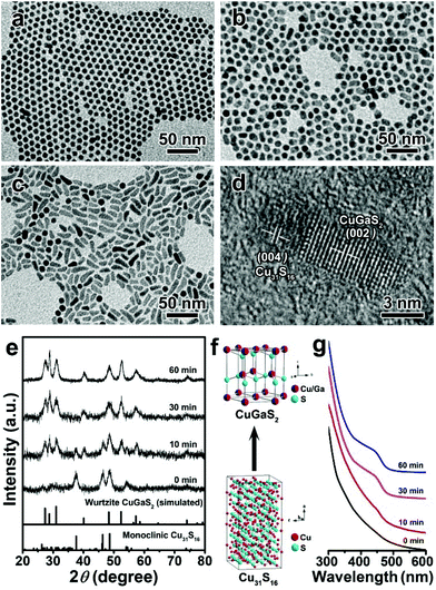 |
| | Fig. 2 TEM images of CGS NCs synthesized at 240 °C for different reaction times: (a) 0 min, (b) 10 min and (c) 30 min; (d) a typical HRTEM image of the HNS obtained at 10 min; (e) the corresponding XRD patterns, the bottom lines represent the diffraction lines of simulated wurtzite CGS and standard monoclinic Cu31S16 (JCPDS no. 23-0959); (f) schematic model of the phase transition from monoclinic Cu31S16 to wurtzite CGS; (g) the corresponding temporal-evolution of the UV-Vis absorption spectra. | |
Apart from the kinetic factors, thermodynamic factors also play a significant role in the cation inter-diffusion, in which the reaction temperature is one of the most important parameters.56–58Fig. 3 depicts the TEM images and XRD patterns of the products synthesized at 200 °C, 220 °C and 250 °C for 60 min, in which the other reaction conditions were kept the same as the products obtained at 240 °C. As shown in Fig. 3a, uniform spherical NCs are obtained at 200 °C, which can be indexed to the pure monoclinic Cu31S16 phase based on the XRD patterns shown in Fig. 3d. Even if the reaction time is prolonged to 240 min, the transition from Cu31S16 nanospheres to 1D CGS NCs is not complete (Fig. S6†). If the reaction temperature is further increased to 220 °C, the predominant samples are 1D nanorods (Fig. 3b). Accordingly, the wurtzite CGS phase is dominant over the XRD patterns shown in Fig. 3d. In contrast to the products obtained at 200 °C, it takes only more than 60 min for the morphology and phase transformation from 0D monoclinic Cu31S16 nanospheres into 1D wurtzite CGS nanorods in the vast majority of products obtained at 220 °C (Fig. S7†). However, it should be noted that there are still a few nanospheres in the products obtained at 120 and 180 min, implying no complete transformation from Cu31S16 into CGS NCs. Moreover, higher reaction temperature (250 °C) brings about the formation of tadpole-shaped NCs with pure wurtzite crystal structures (Fig. 3c and d). Therefore, thermodynamics also contributes to the formation of wurtzite CGS nanorods and higher reaction temperature is beneficial for the Ga3+ ion diffusivity and for providing sufficient energy to overcome the energy barriers, which leads to the inter-diffusion of Ga3+ into the lattice of Cu31S16 to expel the starting phase.56
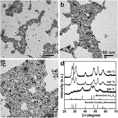 |
| | Fig. 3 TEM images of CGS NCs synthesized at different reaction temperatures: (a) 200 °C; (b) 220 °C; (c) 250 °C; (d) the corresponding XRD patterns, and the bottom lines represent the simulated wurtzite CGS and standard monoclinic Cu31S16 (JCPDS no. 23-0959). | |
Even if the inter-diffusion of Ga3+ is thermodynamically favored, kinetic factors also play an important role in determining the transformation from Cu31S16 into CGS NCs.59 To further demonstrate that such a transformation is a kinetically limited Ga diffusion process, some control experiments were performed. The rate at which the solid-state diffusion can take place is affected by many factors, such as the possibility of cations to diffuse through interstitial sites and the concentration of guest ions.59 As a result, the effects of Ga3+ concentration on the formation of CGS NCs were firstly studied. Considering that higher temperature could bring more energy to overcome the nucleation activation energy barrier and the faster diffusion rate, the reaction temperature was set to 200 °C in this experiment to rule out the effects of thermodynamic factors. The pre-synthesized Cu31S16 nanospheres are selected as seeds, and the different amounts of Ga precursors are then injected into the reaction system, in which the molar ratios of Cu/Ga precursors are kept at 1:1 and 1:5, respectively. The corresponding TEM images and XRD patterns are depicted in Fig. S8 and S9.† When the molar ratio of Cu/Ga precursor is 1:1, the co-existence of Cu31S16 nanospheres and CGS NCs is still observed even if the reaction time is prolonged to 240 and 360 min. Accordingly, some characteristic diffraction peaks of the monoclinic Cu31S16 phase (such as the peaks of 2θ = 37.5° and 46.5°) can also be observed in Fig. S9.† In stark contrast, the Cu31S16 nanospheres disappear after 240 min for the products synthesized at a molar ratio of Cu/Ga precursors of 1:5 (Fig. S8e and S8g†), and no characteristic diffraction peaks assigned to the Cu31S16 phase are observed in the XRD patterns (Fig. S9†), suggesting a complete transformation from binary Cu31S16 NCs into ternary CGS NCs in the presence of a higher concentration of Ga precursors. This result indicates that the inter-diffusion rate of Ga3+ ions to the Cu31S16 NC lattice can be accelerated in the presence of abundant Ga precursors, since the high concentration gradient can keep on driving the inter-diffusion of the Ga3+ ions. To further confirm that the higher concentration gradient could drive the Ga ion flux inward and the Cu ion flux outward, another control experiment was performed by using different DDT dosages to synthesize CGS NCs via a one-pot non-injection method at 250 °C, in which the reaction time was kept at 60 min (Fig. S10†). As a result, less DDT dosage is unfavorable for the inter-diffusion of Ga3+ and brings about the aggregation due to insufficient surface ligands, but a higher DDT dosage can promote the transformation from Cu31S16 into CGS NCs. Even if the reaction temperature is decreased to 200 °C, higher DDT dosage also contributes to the inter-diffusion of Ga3+ (Fig. S11†). Therefore, the complete transformation from Cu31S16 into CGS NCs takes place in the presence of a higher concentration of Ga precursors and a DDT dosage even if the reaction temperature is 200 °C, which confirms to some extent that the formation of CGS NCs is controlled by a kinetically limited Ga diffusion mechanism.60
On the basis of these observations, the reaction-diffusion mechanism is proposed to illustrate the formation of CGS NCs. Once the Cu31S16 NC seeds are formed, which are exposed to a solution of Ga3+ ions, the Ga3+ ions can diffuse into the surface of the Cu31S16 NC lattice via an interstitial and vacancy-assisted mechanism to form a reaction zone. At a later stage, the fast replacement of Cu+ with Ga3+ ions that leads to the nucleation of the product phase takes place at the sites that are energetically allowed. During this step, Cu+ ions are expelled from Cu31S16 NCs through an out-diffusion mechanism, which become solvated gradually by the ligand molecules present in the solution. It should be noted that the precondition of the process is that there is enough energy to complete the inter-diffusion of Ga3+ ions. Once the reaction zone is formed, the inter-diffusion is the rate-limiting process, which often depends on the kinetic factors.
3.3 Synthesis and characterization of quasi-2D CGS nanodisks and 2D CGS nanoplates
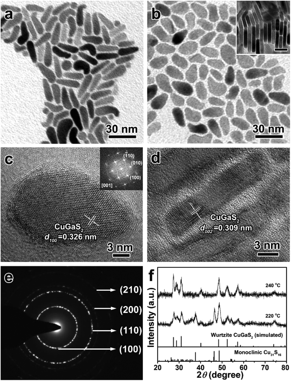
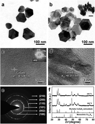
It is well known that the surface ligands often have an important effect on the morphology and phase control of inorganic NCs, because they determine the nucleation and direct the anisotropic growth of the NCs to some extent.61–63 Based on the experimental results mentioned above, DDT plays a vital role in the synthesis of 1D wurtzite CGS nanorods without any other ligands. OM as a versatile reagent is often used in the shape-controlled synthesis of different inorganic NCs. Herein, OM was chosen as a co-ligand to synthesize CGS NCs. Fig. 4 depicts the TEM images and XRD patterns of the as-obtained products in the presence of 5 mL of OM at 220 °C and 240 °C. As shown in Fig. 4a, most of the products obtained at 220 °C exhibit a fat tadpole shape, and a few nanospheres are also confirmed by the XRD results shown in Fig. 4f, in which the featured diffraction peaks of wurtzite CGS and the monoclinic Cu31S16 phase are clearly observed. Even if the reaction time is extended to 180 min, the characteristic peaks of the Cu31S16 phase are still present in the XRD patterns (Fig. S12†). If the reaction temperature is increased to 240 °C, all the products exhibit the shape of a tennis racket (Fig. 4b), whose mean length and width are estimated to be 20.0 ± 1.8 and 10.2 ± 1.4 nm (Fig. S13†), respectively. Moreover, a face-to-face assembly behavior is also observed in the products shown in the inset of Fig. 4b, which is perpendicular to the substrate. The XRD results shown in Fig. 4f reveal the pristine wurtzite CGS crystal structure, which also confirms that higher reaction temperature contributes to the transformation from 0D Cu31S16 nanospheres into quasi-2D wurtzite CGS nanodisks. A typical HRTEM image of a single CGS nanodisk lying on the substrate shown in Fig. 4c shows a clear lattice spacing of 0.326 nm, corresponding to the (100) plane of the wurtzite CGS structure. Moreover, the selected-area fast Fourier transform (FFT) patterns shown in the inset of Fig. 4c show that the angles between three different planes (![[1 with combining macron]](https://www.rsc.org/images/entities/char_0031_0304.gif) 10), (010), and (100) are 60° viewing from the [001] direction, which further confirms that the as-obtained products have a pure wurtzite structure. The HRTEM image of the CGS nanodisk, which is perpendicular to the substrate, is displayed in Fig. 4d, and the d-spacing is measured to be 0.309 nm, which can be assigned to the (002) plane of wurtzite CGS. The SAED pattern shown in Fig. 4e further reveals the hexagonal wurtzite CGS phase, and two brightest rings can be indexed to the (100) and (110) lattice planes. As a matter of fact, in the hexagonal wurtzite structure the {100} facets often have six symmetrical planes, and the {110} facets have four symmetrical planes. If the CGS NCs grow along only one direction, the shape of CGS NCs may be a symmetric hexagon or quadrilateral. According to the previous report, however, the amine molecules prefer to coordinate with cations on the (001) facet of wurtzite NCs, and thus the growth along the [001] direction is prohibited.64 Thus, the growth along the [110] and [100] directions is competitive, and the quasi-2D CGS nanodisks with a tennis-racket section are formed.
10), (010), and (100) are 60° viewing from the [001] direction, which further confirms that the as-obtained products have a pure wurtzite structure. The HRTEM image of the CGS nanodisk, which is perpendicular to the substrate, is displayed in Fig. 4d, and the d-spacing is measured to be 0.309 nm, which can be assigned to the (002) plane of wurtzite CGS. The SAED pattern shown in Fig. 4e further reveals the hexagonal wurtzite CGS phase, and two brightest rings can be indexed to the (100) and (110) lattice planes. As a matter of fact, in the hexagonal wurtzite structure the {100} facets often have six symmetrical planes, and the {110} facets have four symmetrical planes. If the CGS NCs grow along only one direction, the shape of CGS NCs may be a symmetric hexagon or quadrilateral. According to the previous report, however, the amine molecules prefer to coordinate with cations on the (001) facet of wurtzite NCs, and thus the growth along the [001] direction is prohibited.64 Thus, the growth along the [110] and [100] directions is competitive, and the quasi-2D CGS nanodisks with a tennis-racket section are formed.
 |
| | Fig. 4 TEM images of quasi-2D CGS nanodisks synthesized in the presence of 5 mL of OM at (a) 220 °C and (b) 240 °C, and the inset shown in (b) displays the face-to-face assembly of quasi-2D CGS nanodisks (the scale bar is 10 nm); (c and d) typical HRTEM images of the products obtained at 240 °C, (c) lying on the substrate; inset: selected-area FFT pattern; (d) perpendicular to the substrate; (e) SAED pattern of the quasi-2D CGS nanodisks; (f) the corresponding XRD patterns, and the bottom lines represent the diffraction lines of simulated wurtzite CGS and standard monoclinic Cu31S16 (JCPDS no. 23-0959). | |
Our previous report has demonstrated that the anions in the metal precursor could tailor the morphology of CuInS2 NCs, and Cl− ions often played a significant role in the formation of nanoplates.50 Thus, GaCl3 was chosen as the Ga source to synthesize 2D wurtzite CGS nanoplates, in which the other reaction conditions were kept the same as those of 1D CGS nanorods except for GaCl3 in substitution of Ga(acac)3. Fig. 5 shows the TEM images and XRD patterns of the products synthesized at 220 °C and 240 °C, respectively. As shown in Fig. 5a, the hexagonal nanoplates are dominant in the products. Accordingly, the wurtzite CGS structure is the main phase of the products based on the XRD patterns (Fig. 5f). However, the featured peaks of monoclinic Cu31S16 cannot be neglected, which indicates that the transition from Cu31S16 to CGS phase is not complete. To obtain a pure wurtzite CGS phase, the reaction temperature is increased to 240 °C, and thus the 2D wurtzite CGS nanoplates are successfully synthesized with a size range from 50 to 150 nm (Fig. 5b and Fig. S14†). More importantly, no diffraction peaks of the monoclinic Cu31S16 phase are detected in the XRD patterns shown in Fig. 5f, indicating a pure wurtzite CGS phase. Interestingly, a face-to-face self-assembly geometry is also observed, further confirming the formation of nanoplates. The HRTEM image of the 2D CGS nanoplate lying on the substrate and the corresponding selected-area FFT patterns shown in Fig. 5c reveal that the lattice spacing of the (100) plane is 0.328 nm with 60° angles in between different planes including (10), (010), and (100). A typical HRTEM image of the perpendicular section of a 2D CGS nanoplate is shown in Fig. 5d, which exhibits a clear lattice spacing of 0.311 nm, corresponding to the (001) plane of the wurtzite CGS structure. The SAED pattern of 2D CGS nanoplates confirms the hexagonal wurzite structure (Fig. 5e), in which two brightest rings can be indexed to the (100) and (110) planes. Moreover, most of the products have a regular hexagon plate shape, which indicates that the growth direction is along the [100] direction preponderantly. These results mentioned above demonstrate that the incorporation of Cl− ions can effectively tailor the morphology of CGS NCs due to the effect of Cl− ions on the growth process by specific adsorption on the {001} and {110} facets. Therefore, the morphology of wurtzite CGS NCs has been tailored from 1D to 2D by changing the types of surface ligands and the anions in the metal precursors.
 |
| | Fig. 5 TEM images of 2D CGS nanoplates synthesized by using GaCl3 as a Ga source (a) 220 °C and (b) 240 °C, and the inset shows the face-to-face assembly of 2D CGS nanoplates and the scale bar is 100 nm; (c and d) typical HRTEM images of the products obtained at 240 °C, (c) lying on the substrate; inset: selected-area FFT pattern; (d) perpendicular to the substrate; (e) SAED pattern of the 2D CGS nanoplates; (f) the corresponding XRD patterns of samples obtained at 220 °C and 240 °C, and the bottom lines represent the diffraction lines of simulated wurtzite CGS and standard monoclinic Cu31S16 (JCPDS no. 23-0959). | |
3.4 Band structure analysis of different dimensional CGS NCs
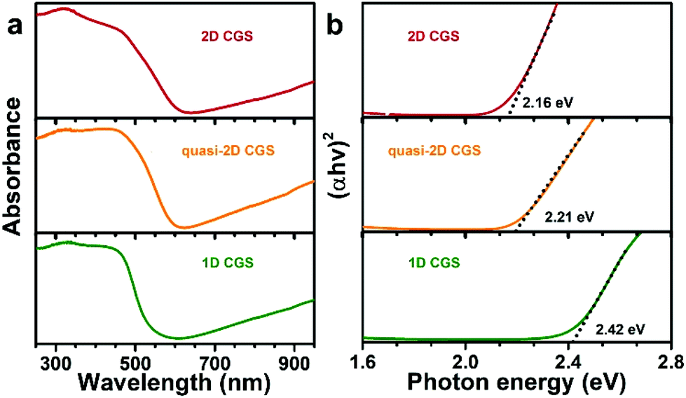
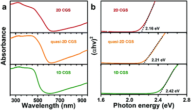
To further understand the optical properties and band structure of the different-shaped CGS NCs, diffuse reflectance spectroscopy (DRS) was employed to study the absorption band onset of the solid NC samples. The reflectance data were converted to absorption based on the Kubelka–Munk function, and the corresponding optical absorption result is given in Fig. 6a. A little red-shift is observed in the absorption onset with the dimension changing from 1D to 2D. To ascertain more accurate measurements, Tauc plots were employed to estimate the energy gaps of the different samples, which can be estimated by extrapolating the linear slope of the plot.23 As shown in Fig. 6b, the optical band gaps can be estimated to be 2.42 eV, 2.21 eV and 2.16 eV for the 1D CGS, quasi-2D CGS and 2D CGS NCs, respectively. Obviously, a decrease of the energy gaps is observed when the dimension is changed from 1D to 2D, which indicates that the optical band gaps become narrow with an increase of the number of dimensions, resulting in an improved capability for utilizing the solar light in the visible range.
 |
| | Fig. 6 (a) Diffuse reflectance spectra (DRS) and (b) the plot of (αhv)2versus the photon energy of different dimensional CGS NCs. | |
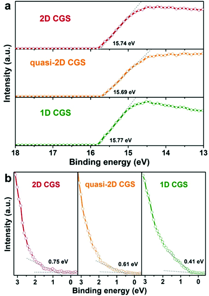
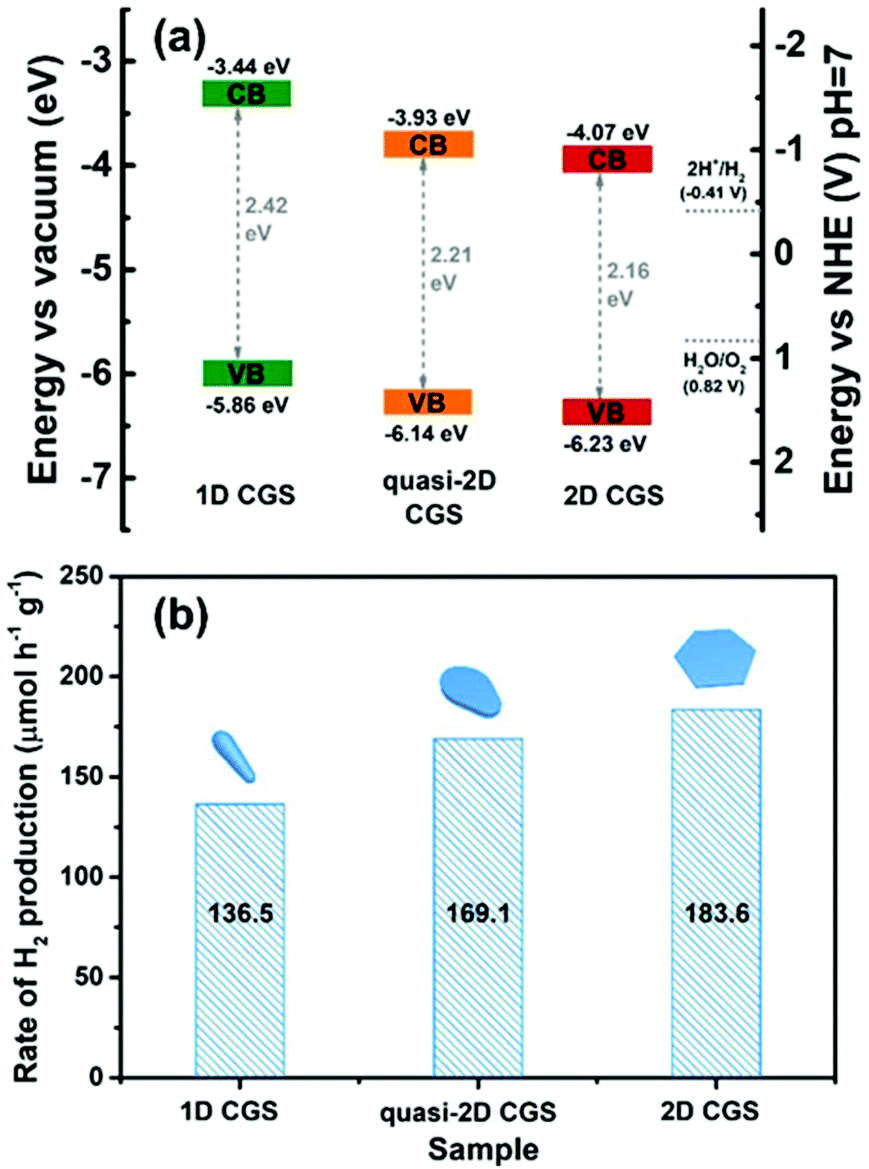
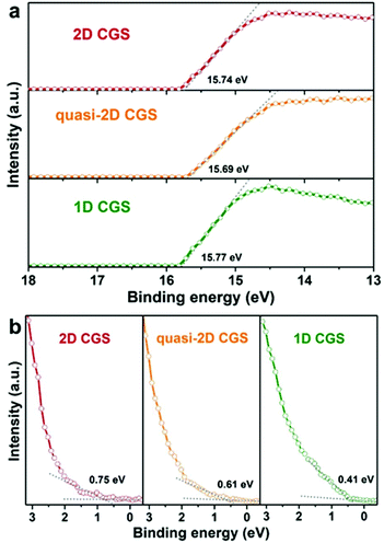
In addition, the electronic structure of wurtzite CGS is calculated by using DFT with Cambridge Serial Total Energy Package (CASTEP) codes, which is helpful to support the experimental results of the optical band gaps. The electronic band structure calculation and computed total density of states (DOS) of the wurtzite CGS are depicted in Fig. S15,† and the calculation result shows a direct semiconductor with a band gap of 2.13 eV at the Γ point, which is very close to the experimental results of 2D wurtzite CGS nanoplates.36 The electronic band structures of different dimensional CGS NCs are studied by the ultraviolet photoelectron spectroscopy (UPS) technique, and the corresponding secondary-electron cut-off and valence-band regions are depicted in Fig. 7a and b, respectively. The valence band maximum (VBM) level can be estimated from the incident photon energy (21.22 eV), the secondary-electron cut-off (Ecut-off) (shown in Fig. 7a), and the onset energy in the valence-band region (Eonset) (shown in Fig. 7b) based on the equation of VBM = 21.22 − (Ecut-off − Eonset). The work function (the difference between vacuum and Femi energy level, ϕ) is calculated from the incident photon energy (21.22 eV), the secondary-electron cut-off (Ecut-off) according to the equation ϕ = 21.22 − Ecut-off. As a result, the work function of the three samples is estimated to be 5.34, 5.53 and 5.48 eV for 1D CGS nanorods, quasi-2D CGS nanodisks and 2D CGS nanoplates, respectively. Obviously, there is little variation in the work function, which suggests that the work function is the intrinsic property of CGS NCs, which is independent of the dimensional change. Moreover, the VBM positions of 1D CGS nanorods, quasi-2D CGS nanodisks and 2D CGS nanoplates are calculated to be 5.86 eV, 6.14 eV, and 6.23 eV below the vacuum level, respectively. As a result, the conduction band minimum (CBM) level can be determined by the optical band gaps and the VBM level, and thus the CBM levels are estimated to be 3.44 eV, 3.93 eV and 4.07 eV below the vacuum level for 1D CGS nanorods, quasi-2D nanodisks and 2D nanoplates, respectively. The detailed UPS parameters including the Ecut-off, Eonset, VBM, bandgap and CBM are summarized in Table 1. A downward shift is observed with the dimension varying from 1D to 2D. Fig. 8a displays the energy level diagram of different dimensional CGS NCs, in which the water reduction and oxidation levels are −4.44 eV and −5.67 eV versus the vacuum level (or −0.41 V and 0.82 V vs. NHE at pH 7 in aqueous solution), respectively. It can be seen that the CBM of CGS NCs is higher than the water reduction level, which indicates that the different samples have photocatalytic activities for water-splitting hydrogen production.65
 |
| | Fig. 7 UPS spectra of (a) high-binding energy secondary-electron cut-off and (b) valence-band edge regions of 1D CGS nanorods, quasi-2D CGS nanodisks and 2D CGS nanoplates. | |
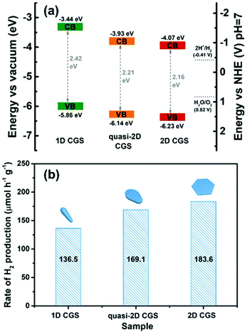 |
| | Fig. 8 (a) The energy level diagrams of 1D CGS nanorods, quasi-2D nanodisks and 2D CGS nanoplates, and the horizontal dotted lines represent the band positions of the redox potentials of water splitting at pH 7 in aqueous solution; (b) the photocatalytic hydrogen production rates of 1D CGS nanorods, quasi-2D nanodisks and 2D CGS nanoplates. | |
Table 1 Summary of energy information of different dimensional CGS NCs obtained from the UPS and absorption results
| Sample |
E
cut-off (eV) |
E
onset (eV) |
VBM (eV) |
Bandgap (eV) |
CBM (eV) |
| VBM and CBM: the value is versus the vacuum level. |
| 1D CGS |
15.77 |
0.41 |
5.86 |
2.42 |
3.44 |
| Quasi-2D CGS |
15.69 |
0.61 |
6.14 |
2.21 |
3.93 |
| 2D CGS |
15.74 |
0.75 |
6.23 |
2.16 |
4.07 |
3.5 Photocatalytic performances of different dimensional CGS NCs
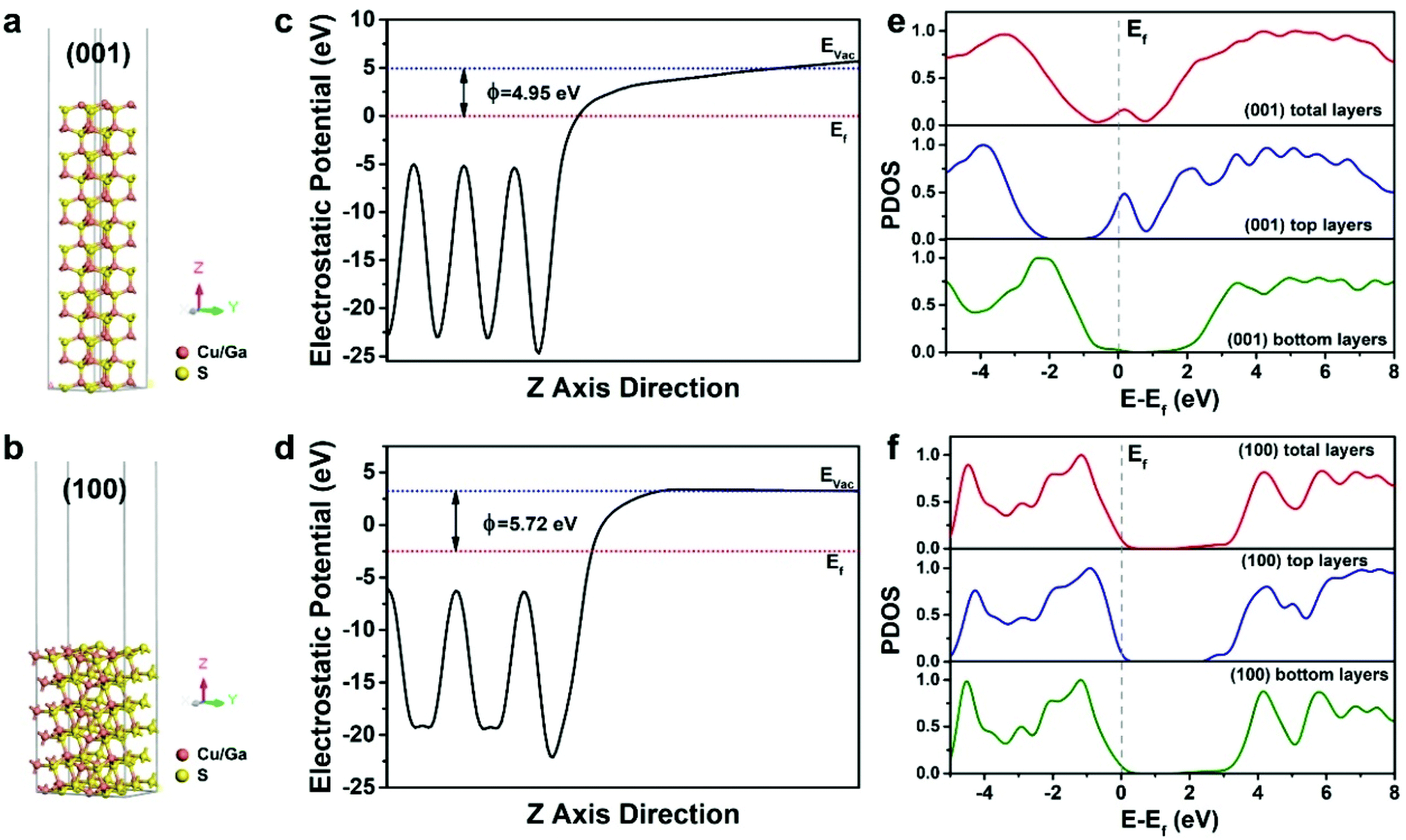
As a proof-of-content demonstration, the photocatalytic hydrogen production of the different dimensional CGS NCs was performed. Since the as-obtained products are hydrophobic, different dimensional CGS NCs were firstly transferred from non-aqueous to water by a pre-established approach, in which 3-mercaptopropanoic acid (MPA) was used as a phase-transfer agent to make the products disperse well in water.46 FTIR spectra were used to characterize the surface change of the products before and after phase transfer, and it is clearly seen that the intensity of the peaks from the –CH2– asymmetric and symmetric stretching vibration becomes weakened (Fig. S16†), which confirmed the substitution of the long-chain organic ligands by the short-chain MPA. The photocatalytic hydrogen evolution of different dimensional CGS NCs was carried out using 15 mg of catalysts in 100 mL of deionized water, in which 0.1 M Na2S and 0.3 M Na2SO3 were used as sacrificial reagents to prohibit the photocorrosion of the photocatalysts. Fig. 8b demonstrates the rate of photocatalytic hydrogen generation for three different samples, and the 2D CGS nanoplates exhibit an improved photocatalytic activity as compared to 1D CGS nanorods and quasi-2D CGS nanodisks. The hydrogen production rate of the 2D CGS nanoplates is estimated to be 183.6 μmol g−1 h−1, which is 1.3 times higher than that of 1D CGS nanorods (136.5 μmol g−1 h−1). The corresponding time-dependent photocatalytic activity shown in Fig. S17† demonstrates that the 2D CGS nanoplates exhibit the best photocatalytic activity at any reaction time. However, in the view of the energy level, the chemical potential of the photo-generated electrons for water reduction reaction is decreased for the 2D CGS nanoplates, whose reduction ability becomes weakened as compared to the other two samples. Therefore, the improved photocatalytic hydrogen evolution of 2D CGS nanoplates may arise from the better charge transport and facet effects. To illustrate such an assumption, on the one hand, electrochemical impedance spectroscopy (EIS) measurements were performed to study the charge transport of different dimensional CGS NCs, and the Nyquist plots of the corresponding three samples indicate that the diameter of the semicircle observed in the 2D CGS nanoplates is smaller than that of 1D and quasi-2D CGS NCs (Fig. S18†). This result suggests that the charge transport resistance of the 2D nanoplates is remarkably reduced, which is beneficial for the improved photocatalytic activity.17,66 On the other hand, the work function and electronic state density of the {001} and {100} facets of wurtzite CGS are analyzed by density functional theory (DFT) calculations, and the schematic illustration of the models for the (001) and (100) surfaces of CGS is depicted in Fig. 9a and b. The work function of the CGS (001) and (100) surfaces is calculated by aligning the Fermi level relative to the vacuum energy level, and the calculation results are given in Fig. 9c and d, respectively. As a result, the work function for the CGS (001) and (100) surfaces is estimated to be 4.95 and 5.72 eV, which implies that it is easier for the electrons escaping from the CGS (001) surface than the CGS (100) surface to the outside environment (vacuum environment). Therefore, the number of photo-generated electrons on the (001) surface is more than that on the (100) surface, which is in favor of the photocatalysis. Fig. 9e and f present the projected density of states (PDOS) of the CGS (001) and (100) surfaces, and the calculation results indicate that the (001) surface has some metal properties, but the (100) surface still maintains the semiconductor property, which suggests that the charge transport of the CGS (001) surface is better than that of the CGS (100) surface theoretically.67,68 Moreover, the electronic structure of different exposed surfaces of CGS further confirms such a deduction (Fig. S19†). Based on the above results, it can be concluded that the improved photocatalytic hydrogen evolution of 2D CGS nanoplates should be attributed to the synergic effects of better charge transport and facet effects of 2D nanoplates.
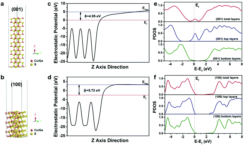 |
| | Fig. 9 Schematic models of the (a) (001) surface and (b) (100) surface of stimulated wurtzite CGS after geometry optimization. The red and yellow spheres represent copper/gallium and sulfur, respectively; work function for the (c) CGS (001) surface and (d) (100) surface. EVac, Ef and ϕ are the vacuum level, Fermi level and work function, respectively; the calculated PDOS for (e) CGS (001) and (f) (100) surfaces, where the PDOS contains the total layer surface, top layer surface and bottom layer surface for simulated every surface. The gray dash represents Fermi levels of the corresponding CGS surface. | |
4. Conclusion
In summary, a non-injection synthesis approach has been developed to prepare ternary wurtzite CGS NCs, in which the morphology can be tuned from 1D nanorods to 2D nanoplates by varying the surface ligands and anion types in metal precursors. The optical band gap and electronic structure are in correlation with the dimensions of the different-shaped CGS NCs. The formation mechanism of 1D CGS nanorods is studied by the temporal evolution of the morphology and crystal structure, which starts with the nucleation of monoclinic Cu31S16, followed by the inter-diffusion of Ga3+ into the lattice to form Cu31S16–CGS HNS and finally 1D CGS nanorods are formed. The 2D wurtzite CGS nanoplates prefer to expose the {001} facets but the 1D wurtzite CGS nanorods have more exposed {100} facets. Since the CGS (001) surface offers more photo-generated electrons and charge transport, the 2D CGS nanoplates show an improved photocatalytic hydrogen production under simulated solar illumination as compared to the 1D CGS nanorods and quasi-2D CGS nanodisks. This work provides an effective approach for enhancing the photocatalytic activity of multinary copper based semiconductor NCs through tuning the dimension.
Conflicts of interest
There are no conflicts to declare.
Acknowledgements
This work was partly supported by the National Natural Science Foundation of China (No. 61735004, 61674011, 21507074, 21503209 and 21603011) and the Beijing Natural Science Foundation (No. 4172050). The authors (Z. W. and S. Q.) appreciate the National Key Research and Development Program of China (No. 2017YFA0206600) and the Key Research Program of Frontier Science, Chinese Academy of Sciences (No. QYZDB-SSW-SLH006). The author (A. T.) appreciates the support from the “Excellent One Hundred” project of Beijing Jiaotong University.
Notes and references
- V. L. Colvin, M. C. Schlamp and A. P. Alivisatos, Nature, 1994, 370, 354–357 CrossRef CAS.
- Y. Yang, Y. Zheng, W. Cao, A. Titov, J. Hyvonen, J. R. Manders, J. Xue, P. H. Holloway and L. Qian, Nat. Photonics, 2015, 9, 259–266 CrossRef CAS.
- A. Tang, S. Qu, F. Teng, Y. Hou, Y. Wang and Z. Wang, J. Nanosci. Nanotechnol., 2011, 11, 9384–9394 CrossRef CAS.
- Y. L. Lee and Y. S. Lo, Adv. Funct. Mater., 2009, 19, 604–609 CrossRef.
- S. Ma, Y. Deng, J. Xie, K. He, W. Liu, X. Chen and X. Li, Appl. Catal., B, 2018, 227, 218–228 CrossRef CAS.
- Q. Li, X. Li, S. Wageh, A. A. Al-Ghamdi and J. Yu, Adv. Energy Mater., 2015, 5, 1500010 CrossRef.
- S. A. McDonald, G. Konstantatos, S. Zhang, P. W. Cyr, E. J. D. Klem, L. Levina and E. H. Sargent, Nat. Mater., 2005, 4, 138–142 CrossRef CAS PubMed.
- L. Li, Z. Lou and G. Shen, ACS Appl. Mater. Interfaces, 2015, 7, 23507–23514 CrossRef CAS PubMed.
- C. Coughlan, M. Ibáñez, O. Dobrozhan, A. Singh, A. Cabot and K. M. Ryan, Chem. Rev., 2017, 117, 5865–6109 CrossRef CAS PubMed.
- J. Kolny-Olesiak and H. Weller, ACS Appl. Mater. Interfaces, 2013, 5, 12221–12237 CrossRef CAS PubMed.
- C. Zou, L. Zhang, L. Zhai, D. Lin, J. Gao, Q. Li, Y. Yang, X. Chen and S. Huang, Chem. Commun., 2011, 47, 5256–5258 RSC.
- Z. Liu, A. Tang, M. Wang, C. Yang and F. Teng, J. Mater. Chem. C, 2015, 3, 10114–10120 RSC.
- M. Lv, J. Zhu, Y. Huang, Y. Li, Z. Shao, Y. Xu and S. Dai, ACS Appl. Mater. Interfaces, 2015, 7, 17482–17488 CrossRef CAS PubMed.
- B. Chen, H. Zhong, M. Wang, R. Liu and B. Zou, Nanoscale, 2013, 5, 3514–3519 RSC.
- J.-H. Kim and H. Yang, Chem. Mater., 2016, 28, 6329–6335 CrossRef CAS.
- X.-B. Fan, S. Yu, F. Zhan, Z.-J. Li, Y.-J. Gao, X.-B. Li, L.-P. Zhang, Y. Tao, C.-H. Tung and L.-Z. Wu, ChemSusChem, 2017, 10, 4833–4838 CrossRef CAS PubMed.
- L. Tan, Y. Liu, B. Mao, B. Luo, G. Gong, Y. Hong, B. Chen and W. Shi, Inorg. Chem. Front., 2018, 5, 258–265 RSC.
- B. Chen, H. Zhong, W. Zhang, Z. Tan, Y. Li, C. Yu, T. Zhai, Y. Bando, S. Yang and B. Zou, Adv. Funct. Mater., 2012, 22, 2081–2088 CrossRef CAS.
- W.-C. Huang, C.-H. Tseng, S.-H. Chang, H.-Y. Tuan, C.-C. Chiang, L.-M. Lyu and M. H. Huang, Langmuir, 2012, 28, 8496–8501 CrossRef CAS PubMed.
- Z. Pan, I. More-Seró, Q. Shen, H. Zhang, Y. Li, K. Zhao, J. Wang, X. Zhong and J. Bisquert, J. Am. Chem. Soc., 2014, 136, 9203–9210 CrossRef CAS PubMed.
- S. T. Connor, C.-M. Hsu, B. D. Weil, S. Aloni and Y. Cui, J. Am. Chem. Soc., 2009, 131, 4962–4966 CrossRef CAS PubMed.
- M. Kruszynska, H. Borchert, J. Parisi and J. Kolny-Olesiak, J. Am. Chem. Soc., 2010, 132, 15976–15986 CrossRef CAS PubMed.
- Y.-H. A. Wang, X. Zhang, N. Bao, B. Lin and A. Gupta, J. Am. Chem. Soc., 2011, 133, 11072–11075 CrossRef CAS PubMed.
- M. Han, X. Zhang and Z. Zeng, RSC Adv., 2014, 4, 62380–62386 RSC.
- J. Hashemi, A. Akbari, S. Huotari and M. Hakala, Phys. Rev. B: Condens. Matter, 2014, 90, 075154 CrossRef.
- J.-H. Kim, D.-Y. Jo, K.-H. Lee, E.-P. Jang, C.-Y. Han, J.-H. Jo and H. Yang, Adv. Mater., 2016, 28, 5093–5098 CrossRef CAS PubMed.
- D.-Y. Jo and H. Yang, Chem. Commun., 2016, 52, 709–712 RSC.
- M. Zhao, F. Huang, H. Lin, J. Zhou, J. Xu, Q. Wu and Y. Wang, Nanoscale, 2016, 8, 16670–16676 RSC.
- T. A. Kandiel, D. H. Anjum, P. Sautet, T. L. Bahers and K. Takanabe, J. Mater. Chem. A, 2015, 3, 8896–8904 RSC.
- Q. Lu, J. Hu, K. Tang, Y. Qian, G. Zhou and X. Liu, Inorg. Chem., 2000, 39, 1606–1607 CrossRef CAS PubMed.
- J. Zhong, Y. Zhao, H. Yang, J. Wang, X. Liang and W. Xiang, Appl. Surf. Sci., 2011, 257, 10188–10194 CrossRef CAS.
- J. Q. Hu, B. Deng, C. R. Wang, K. B. Tang and Y. T. Qian, Solid State Commun., 2002, 121, 493–496 CrossRef CAS.
- Y. Zhai, J. C. Flanagan and M. Shim, Chem. Mater., 2017, 29, 6161–6176 CrossRef CAS.
- H.-T. Tung, Y. Hwu, I.-G. Chen, M.-G. Tsai, J.-M. Song, I. M. Kempson and G. Margaritondo, Chem. Commun., 2011, 47, 9152–9154 RSC.
- N. Xiao, L. Zhu, K. Wang, Q. Dai, Y. Wang, S. Li, Y. Sui, Y. Ma, J. Liu, B. Liu, G. Zou and Bo. Zou, Nanoscale, 2012, 4, 7443–7447 RSC.
- Z. Liu, Q. Hao, R. Tang, L. Wang and K. Tang, Nanoscale Res. Lett., 2013, 8, 524 CrossRef PubMed.
- S. D. Adhikari, A. Dutta, G. Prusty, P. Sahu and N. Pradhan, Chem. Mater., 2017, 29, 5384–5393 CrossRef CAS.
- S.-H. Chang, B.-C. Chiu, T.-L. Gao, S.-L. Jheng and H.-Y. Tuan, CrystEngComm, 2014, 16, 3323–3330 RSC.
- M. D. Regulacio, C. Ye, S. H. Lim, Y. Zheng, Q.-H. Xu and M.-Y. Han, CrystEngComm, 2013, 15, 5214–5217 RSC.
- M.-Y. Huang, X.-B. Li, Y.-J. Gao, J. Li, H.-L. Wu, L.-P. Zhang, C.-H. Tung and L.-Z. Wu, J. Mater. Chem. A, 2018, 6, 6015–6021 RSC.
- Y. Chen, S. Zhao, X. Wang, Q. Peng, R. Lin, Y. Wang, R. Shen, X. Cao, L. Zhang, G. Zhou, J. Li, A. Xia and Y. Li, J. Am. Chem. Soc., 2016, 138, 4286–4289 CrossRef CAS PubMed.
- T.-T. Zhuang, Y. Liu, M. Sun, S.-L. Jiang, M.-W. Zhang, X.-C. Wang, Q. Zhang, J. Jiang and S.-H. Yu, Angew. Chem., Int. Ed., 2015, 54, 11495–11500 CrossRef CAS PubMed.
- O. Stroyuk, A. Raevskaya and N. Gaponik, Chem. Soc. Rev., 2018, 47, 5354–5422 RSC.
- H. Kaga, Y. Tsutsui, A. Nagane, A. Iwase and A. Kudo, J. Mater. Chem. A, 2015, 3, 21815–21823 RSC.
- D. Zhu, A. Tang, H. Ye, M. Wang, C. Yang and F. Teng, J. Mater. Chem. C, 2015, 3, 6686–6691 RSC.
- X. Yu, A. Shavel, X. An, Z. Luo, M. Ibańez and A. Cabot, J. Am. Chem. Soc., 2014, 136, 9236–9239 CrossRef CAS.
- S. J. Clark, M. D. Segall, C. J. Pickard, P. J. Hasnip, M. I. J. Probert, K. Refson and M. C. Payne, Z. Kristallogr., 2005, 220, 567–570 CAS.
-
W. Yang and R. G. Parr, Density-functional theory of atoms and molecules, Oxford University Press, 1989 Search PubMed.
- J. P. Perdew, K. Burke and M. Ernzerhof, Phys. Rev. Lett., 1996, 77, 3865 CrossRef CAS PubMed.
- A. Tang, Z. Hu, Z. Yin, H. Ye, C. Yang and F. Teng, Dalton Trans., 2015, 44, 9251–9259 RSC.
- J. Li, M. Bloemen, J. Parisi and J. Kolny-Olesiak, ACS Appl. Mater. Interfaces, 2014, 6, 20535–20543 CrossRef CAS PubMed.
- X. Lu, Z. Zhuang, Q. Peng and Y. Li, CrystEngComm, 2011, 13, 4039–4045 RSC.
- D. Pan, L. An, Z. Sun, W. Hou, Y. Yang, Z. Yang and Y. Lu, J. Am. Chem. Soc., 2008, 130, 5620–5621 CrossRef CAS PubMed.
- K. Idczak, P. Mazur, S. Zuber, L. Markowski, M. Skiścim and S. Bilińska, Appl. Surf. Sci., 2014, 304, 29–34 CrossRef CAS.
- S.-K. Han, C. Gu, S. Zhao, S. Xu, M. Gong, Z. Li and S.-H. Yu, J. Am. Chem. Soc., 2016, 138, 12913–12919 CrossRef CAS PubMed.
- H.-C. Liao, M.-H. Jao, J.-J. Shyue, Y.-F. Chen and W.-F. Su, J. Mater. Chem. A, 2013, 1, 337–341 RSC.
- Y. Yuan, Z. Liu, Z. Liu, L. Peng, Y. Li and A. Tang, Appl. Surf. Sci., 2017, 405, 280–288 CrossRef CAS.
- Y. Xia, X. Xia and H. Peng, J. Am. Chem. Soc., 2015, 137, 7947–7966 CrossRef CAS PubMed.
- L. D. Trizio and L. Manna, Chem. Rev., 2016, 116, 10852–10887 CrossRef PubMed.
- L. Mu, F. Wang, B. Sadtler, R. A. Loomis and W. E. Buhro, ACS Nano, 2015, 9, 7419–7428 CrossRef CAS PubMed.
- D. Zhu, A. Tang, L. Peng, Z. Liu, C. Yang and F. Teng, J. Mater. Chem. C, 2016, 4, 4880–4888 RSC.
- Y. Liu, A. Tang, Q. Zhang and Y. Yin, J. Am. Chem. Soc., 2015, 137, 11327–11339 CrossRef CAS PubMed.
- P. Reiss, M. Carrière, C. Lincheneau, L. Vaure and S. Tamang, Chem. Rev., 2016, 116, 10731–10819 CrossRef CAS PubMed.
- Y. Cheng, Y. Wang, F. Bao and D. Chen, J. Phys. Chem. B, 2006, 110, 9448–9451 CrossRef CAS PubMed.
- P. Zhou, J. Yu and M. Jaroniec, Adv. Mater., 2014, 26, 4920–4935 CrossRef CAS PubMed.
- S. Ma, X. Xu, J. Xie and X. Li, Chin. J. Catal., 2017, 38, 1970–1980 CrossRef CAS.
- Y. Yang, D.-M. Tang, C. Zhang, Y. Zhang, Q. Liang, S. Chen, Q. Weng, M. Zhou, Y. Xue, J. Liu, J. Wu, Q. H. Cui, C. Lian, G. Hou, F. Yuan, Y. Bando, D. Golberg and X. Wang, Energy Environ. Sci., 2017, 10, 979–986 RSC.
- M. M. Han, X. L. Zhang and Z. Zeng, RSC Adv., 2016, 6, 110511–110516 RSC.
Footnotes |
| † Electronic supplementary information (ESI) available. See DOI: 10.1039/c8nr07353h |
| ‡ Current address: Department of Chemistry, University of Central Florida, Orlando 32816, USA. |
|
| This journal is © The Royal Society of Chemistry 2019 |
Click here to see how this site uses Cookies. View our privacy policy here. 
 bc,
Yanbin
Huang
bc,
Jing
Li
d,
Yi
Yuan
a,
Haihang
Ye‡
a,
Dongxu
Zhu
a,
Zhijie
Wang
bc,
Yanbin
Huang
bc,
Jing
Li
d,
Yi
Yuan
a,
Haihang
Ye‡
a,
Dongxu
Zhu
a,
Zhijie
Wang