
Ultrahigh-efficiency aqueous flat nanocrystals of CdSe/CdS@Cd1−xZnxS colloidal core/crown@alloyed-shell quantum wells†
Sushant
Shendre
 a,
Savas
Delikanli
*abc,
Mingjie
Li
b,
Didem
Dede
c,
Zhenying
Pan
de,
Son Tung
Ha
de,
Yuan Hsing
Fu
d,
Pedro L.
Hernández-Martínez
ac,
Junhong
Yu
a,
Onur
Erdem
c,
Arseniy I.
Kuznetsov
de,
Cuong
Dang
af,
Tze Chien
Sum
b and
Hilmi Volkan
Demir
*abc
a,
Savas
Delikanli
*abc,
Mingjie
Li
b,
Didem
Dede
c,
Zhenying
Pan
de,
Son Tung
Ha
de,
Yuan Hsing
Fu
d,
Pedro L.
Hernández-Martínez
ac,
Junhong
Yu
a,
Onur
Erdem
c,
Arseniy I.
Kuznetsov
de,
Cuong
Dang
af,
Tze Chien
Sum
b and
Hilmi Volkan
Demir
*abc
aLUMINOUS! Centre of Excellence for Semiconductor Lighting and Displays, School of Electrical and Electronic Engineering, Nanyang Technological University, Singapore 639798. E-mail: sdelikanli@ntu.edu.sg; hvdemir@ntu.edu.sg
bSchool of Physical and Mathematical Sciences, Nanyang Technological University, Singapore 639798
cDepartment of Electrical and Electronics Engineering and Department of Physics, UNAM-Institute of Materials Science and Nanotechnology, Bilkent University, Bilkent, Ankara, Turkey 06800. E-mail: volkan@bilkent.edu.tr
dData Storage Institute, A*STAR (Agency for Science, Technology and Research), Singapore 138634
eInstitute of Materials Research and Engineering, A*STAR (Agency for Science, Technology and Research), Singapore, 138634
fCINTRA UMI CNRS/NTU/THALES, Research Techno Plaza, Nanyang Technological University, Singapore 637553
First published on 5th November 2018
Abstract
Colloidal semiconductor nanoplatelets (NPLs) are highly promising luminescent materials owing to their exceptionally narrow emission spectra. While high-efficiency NPLs in non-polar organic media can be obtained readily, NPLs in aqueous media suffer from extremely low quantum yields (QYs), which completely undermines their potential, especially in biological applications. Here, we show high-efficiency water-soluble CdSe/CdS@Cd1−xZnxS core/crown@shell NPLs formed by layer-by-layer grown and composition-tuned gradient Cd1−xZnxS shells on CdSe/CdS core/crown seeds. Such control of shell composition with monolayer precision and effective peripheral crown passivation, together with the compact capping density of short 3-mercaptopropionic acid ligands, allow for QYs reaching 90% in water, accompanied by a significantly increased photoluminescence lifetime (∼35 ns), indicating the suppression of nonradiative channels in these NPLs. We also demonstrate the controlled attachment of these NPLs without stacking at the nanoscale by taking advantage of their 2D geometry and hydrophilicity. This is a significant step in achieving controlled assemblies and overcoming the stacking process, which otherwise undermines their film formation and performance in optoelectronic applications. Moreover, we show that the parallel orientation of such NPLs achieved by the controlled attachment enables directed emission perpendicular to the surface of the NPL films, which is highly advantageous for light extraction in light-emitting platforms.
Introduction
Colloidal semiconductor nanocrystals (NCs) have a wide range of applications in energy harvesting, lighting and display technologies as well as in the biological fields.1–4 Among them water-based semiconductor nanocrystals are particularly attractive for biological labelling and bio-imaging applications thanks to their impressive photostability and size-dependent, color-saturated emission compared to organic dyes and fluorescent proteins.5–8 For this purpose, there is a strong need for developing high photoluminescence (PL) efficiency, solution-processed colloidal emitters that are stable in an aqueous environment. A typical method used for preparing aqueous NCs is to synthesize them in organic solvents and then transfer them to water via ligand exchange.9,10 Water-soluble CdTe-based colloidal quantum dots (QDs) have been developed with PL QYs >80% in the visible range.11,12 However, similar results for CdSe-based QDs have been difficult to achieve due to the PL quenching after ligand exchange.13,14 Recently, NCs of different dimensionalities including nanorods, nanoplatelets (NPLs) and dot-in-rod structures have also made their entries in the family of water-soluble nanomaterials having attractive applications.15–17Colloidal NPLs, which have been most recently introduced among all other types of NCs, are atomically flat semiconductor NCs having tight quantum confinement only in the thickness direction, as their lateral sizes are typically larger than the exciton Bohr radius.18,19 NPLs offer an exceptionally narrow PL spectral line width due to the absence of inhomogeneous broadening20 and provide unprecedented opportunities for the design of advanced heterostructures owing to the possibility of growing laterally a crown and vertically a shell selectively unlike the QDs, which are limited by only shell growth.21–25 Their emission efficiencies and stability can be improved significantly with either a wide bandgap crown or shell, or a combination of both.21,26–28 While a crown helps to passivate the exciton quenching sites on the periphery resulting in a high PL QY, a shell is required to increase their photostability and chemical robustness. By designing CdSe/CdS@CdS core/crown@shell NPLs resembling a ‘platelet-in-box’ structure, Kelestemur et al.25 obtained NPLs with PL QY levels of ∼40% showing highly stable amplified spontaneous emission with a low optical gain threshold. With large oscillator strengths, bright narrowband emission and fast PL decay lifetimes, NPLs are highly appealing candidates for next-generation quantum emitters in biological and other applications. NPLs soluble in non-polar media have been extensively investigated and high quantum yields have been reported.21,29–31 However, water-soluble NPLs have suffered from an extremely low PL QY, although aqueous NPLs present a great platform especially for biological labelling. It was previously reported that the PL QYs of the core and core/crown NPLs are significantly reduced when transferred to aqueous media due to the extreme sensitivity of the excitonic recombination to the surface passivation and environment.32 Similar quenching of PL QY after ligand exchange is also commonly observed in QDs.13,33 Lim et al.17 reported that the PL QY of core/shell NPLs in aqueous media is also limited to only a few percent, and although these water-based core/shell NPLs could be very attractive for biomolecular labelling owing to their rapid cellular entry compared to QDs and multiplexed imaging by virtue of a narrow PL full-width-at-half-maximum (fwhm), the efficiency challenge completely undermines their potential. Therefore, it is vital to achieve highly efficient NPLs in aqueous media for their exploitation in biological and optoelectronic applications, which has not been possible to date.
In this work, to address this pivotal requirement of high quantum efficiency, we present highly efficient CdSe/CdS@Cd1−xZnxS hetero-NPLs in both organic and aqueous systems in core/crown@shell architecture using colloidal atomic layer deposition (c-ALD). This approach allowed us to precisely control the alloying of Cd and Zn at the monolayer level. The PL QY of the engineered aqueous NPLs reaches 90%, significantly outperforming the QY of all previously reported aqueous colloidal QWs, which are in the few percent range.17,32 The significantly long PL lifetime (∼35 ns) measured for the aqueous NPLs accompanied by a high PL QY indicates the effective passivation of nonradiative channels in this system. In addition, here we show the controlled and patterned attachment of the aqueous NPLs on the nanoscale by exploiting their 2D geometry and hydrophilicity on functionalized substrates. Such nanopatterned thin films of these NPLs obtained by the controlled attachment technique allow for directed emission perpendicular to the surface of the films, which is highly advantageous for light extraction for example in light emitting and custom imaging/lasing platforms.
Results and discussion
The proposed schematic structure of our aqueous core/crown@shell NPLs is shown in Fig. 1(a). The CdSe/CdS core/shell heterostructure has a quasi-type-II band structure in which the electron wavefunction is delocalized over the nanocrystal due to the small conduction band-offset as presented in Fig. 1(b),34,35 while the CdSe/ZnS core/shell heterostructure has a type-I band structure which better isolates the excitons formed in the core from the surface. In the case of NPLs, there is a substantial leakage of the carrier wave functions into the shell,29 due to the extreme nature of the vertical confinement, leading to a red shift in the PL emission peak even with the growth of a ZnS shell.28 Compared to CdS having a lattice mismatch of only ∼4%, the significantly large lattice mismatch between CdSe and ZnS, which is ∼12%, leads to the formation of defects at the core–shell interface due to the lattice strain, which would potentially decrease the QY.35 Thus, an interfacial alloying between the core and the shell is required to relax this strain effectively. The gradient composition shell growth also suppresses the fast nonradiative Auger recombination of excitons.36,37 In the synthesis of colloidal quantum dots, having a buffer interlayer between the core–shell or a gradient composition leads to an increase in QYs and robustness.35,38,39 To achieve the interfacial alloying in our NPLs we used the c-ALD22 technique to grow Cd1−xZnxS shells layer by layer on top of the core/crown CdSe/CdS NPLs with a gradual increase in Zn concentration. The detailed synthesis steps are provided in the ESI.†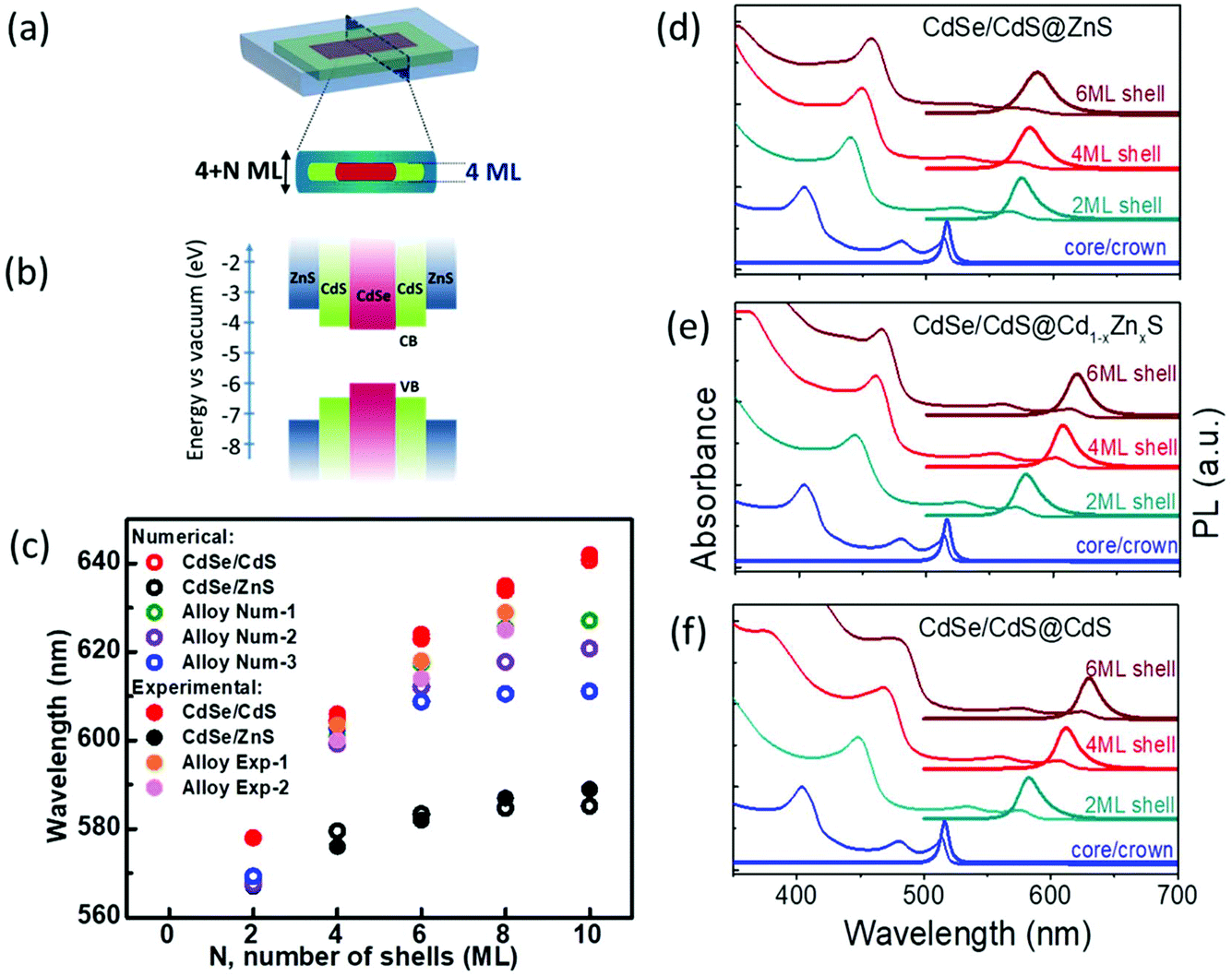 | ||
| Fig. 1 Emission and absorption characteristics of CdSe/CdS@Cd1−xZnxS core/crown@shell NPLs. (a) A schematic structure of the proposed core/crown@shell NPLs where N represents the number of shell layers on top of 4 ML core/crown seeds; (b) the energy band diagram showing the relative positions of CdSe, CdS and ZnS bandgaps; and (c) calculated energies (open circle symbol) of the heavy hole transitions of CdSe/Cd1−xZnxS core/shell NPLs, by solving the stationary Schrödinger equation considering the effective mass approximation. The different ‘x’ values in Cd1−xZnxS for N = 2, 4, 6, 8, and 10 MLs of shell, respectively, in different alloy shell samples are: Alloy Num-1: (x = 0.10, 0.18, 0.33, 1.00, 1.00), Alloy Num-2: (x = 0.2, 0.4, 0.6, 0.8, 1.0), and Alloy Num-3: (x = 0, 1, 1, 1, 1). The solid circle symbols represent the energy of the heavy hole transitions from the experimental results. (d)–(f) The absorbance and PL spectra of NPLs with (d) Zn-only, (e) gradient alloy, and (f) Cd-only shells on top of CdSe/CdS core/crown NPLs. | ||
Fig. 1(d)–(f) present the PL and absorbance spectra of three types of shells grown on top of the same starting core/crown NPLs. These show the optical spectra of the NPLs dispersed in N-methylformamide (NMF) having 2, 4 and 6 monolayer (ML) shells consisting exclusively of CdS, ZnS and gradient composition Cd1−xZnxS deposited on 4 ML core/crown CdSe/CdS NPLs. We consider the deposition of one layer each of anion and cation on both the lateral facets of NPLs as a growth of 2 MLs (illustrated by N in Fig. 1(a)). It can be seen that with each additional 2 MLs of the shell deposition, there is a red shift in the absorbance and PL emission peak with respect to the peak positions of the core/crown NPLs. Our core/crown seeds have a PL peak at 516 nm with a fwhm of 8 nm (∼37 meV) with a PL QY of ∼50% in hexane. This red shift is the largest for the CdS-only shells and the smallest for the ZnS-only shells, whereas the alloyed shells produce a red shift in between the extremes of the CdS and ZnS shells depending on the extent of alloying indicating the difference in the degrees of excitonic confinement. The PL peak of the NPLs having 2 ML CdS shells is located at 583 nm with a fwhm of 21 nm (∼77 meV), which red shifts to 630 nm with a fwhm of 20 nm (∼61 meV) upon depositing 6 ML of CdS shells. The PL peak after the deposition of 2 ML ZnS shells appears at 575 nm with a fwhm of 22 nm (∼81 meV), red shifting to 588 nm with a fwhm of 28 nm (∼100 meV) upon the deposition of 6 ML of ZnS shells. The strong red shift of absorption and emission peaks with the growth of CdS shells is consistent with previous observations, which is associated with the relaxation of the carrier wavefunctions, largely electrons, into the shell layers due to the extreme confinement experienced in the NPL cores and the small band offsets between CdSe and CdS.29 The increase in fwhm of the PL spectra upon the deposition of shells is associated with the increase in exciton–phonon coupling in the shell.29 Alternatively, the larger fwhm for pure ZnS shells compared with pure CdS shells indicates greater inhomogeneity during shell deposition possibly due to the higher lattice mismatch.
We calculated the energy of heavy hole transitions (responsible for the PL emission) in core-(multi)shell NPLs by considering the problem of particle in a box and using the stationary Schrödinger equation with effective mass approximation. The details of our theoretical calculations are given in the ESI.† In the case of multiple CdS shells, we observed a strong red shift closely matching the experimental results as shown in Fig. 1(c). In the case of multiple ZnS shells, the red shift of the heavy hole transition saturates very quickly after adding only 6 MLs of ZnS shells at 583 nm due to the large band offsets between CdSe and ZnS. This is close to our experimental results for the NPLs having only ZnS shells showing the saturation of the heavy hole transition at ∼587 nm. In the case of alloyed shells, we computed the energy of the heavy hole transition in the samples having different gradiently-varying compositions of shells. The calculated energy values stay between the energies of samples having only CdS and only ZnS multiple shells as expected and our results from the calculations are in excellent agreement with the experimental results as presented in Fig. 1(c). In all the core/multi-shell NPL structures, the holes remain confined to the core due to the large potential barrier across the core–shell interface (>0.5 eV) (ESI, Fig. S16†). On the other hand, the electron becomes significantly more confined to the core leading to a blue shift in the excitonic transitions, as the Zn concentration is increased. The reason for this behaviour stems from the fact that the potential barrier at the core–shell interface increases from 0.1 to 0.7 eV, which in turn converts the quasi-type-II structure into type-I, as the Zn concentration changes from 0 to 1. As can be seen from the calculations, alloying provides a pathway for tuning the optical properties of the core/shell NPLs having discrete energy levels associated with their magic size thickness.
Table 1 provides a comparison among the PL QYs of different monolayers of CdS, ZnS and Cd1−xZnxS shells grown on the core/crown NPLs in NMF. All of the samples with only CdS shells have a PL QY in the range of 10–15%. However, the PL QYs of samples with ZnS shells are in the range of 15–30%, being higher than the samples with CdS shells, which can be attributed to the increased electronic isolation from the surface, thanks to the large band offset between CdSe and ZnS (see ESI, Fig. S15†).
| Total 4 + N monolayers | Pure-Cd shells | Pure-Zn shells | Combination of pure-Cd and pure-Zn shells | Gradient alloy shell (A-p-q-r-t-w) | |
|---|---|---|---|---|---|
| N = 4 | C–C | Z–Z | C–Z | A-7-3 | |
| <15% | <30% | <40% | <50% | ||
| N = 6 | C–C–C | Z–Z–Z | C–C–Z | C–Z–Z | A-7-3-1 |
| <15% | <25% | <35% | <45% | <60% | |
| N = 8 | C–C–C–C | Z–Z–Z–Z | C–C–Z–Z | C–Z–Z–Z | A-7-3-1-0 |
| <10% | <15% | <30% | <35% | <45% | |
| N = 10 | C–C–C–C–C | Z–Z–Z–Z–Z | C–C–Z–Z–Z | A-7-3-1-0-0 | |
| <10% | <15% | <25% | <35% | ||
To allow for a smooth transition of lattice matching between the core and the shell, we grew ZnS shells on NPLs having CdS shells to form combinations of CdS and ZnS multi-shell heterostructures. This strategy indeed resulted in an important increase in PL QY up to 45%. It is thus expected that an enhanced level of QY can be obtained by carefully controlling the gradual change in the shell composition by using a gradient alloy of Cd1−xZnxS. The best of these samples having the gradient alloy of Cd1−xZnxS shells, obtained by increasing the Zn![[thin space (1/6-em)]](https://www.rsc.org/images/entities/char_2009.gif) :Cd composition ratio in the successive shell layers, exhibits a PL QY in NMF in the range of 55–60%, which is substantially higher than the QY of NPLs possible with CdS-only or ZnS-only shells. We obtained such a high PL QY with narrow emission by further optimizing the mixture of Zn:Cd ratio in the precursors, the exact composition of which we shall discuss shortly. The PL QY maximizes near 4 or 6 ML shells and then reduces upon the deposition of additional shell layers. In previous reports also, a decrease in PL QY with increasing shell thickness was observed and attributed to the increasing defect densities with thicker shells, especially in the case of high Zn content.25,28 In addition to this, the emission can be tuned over a wide spectral range by changing the Zn:Cd content ratio and/or the number of shell layers.
:Cd composition ratio in the successive shell layers, exhibits a PL QY in NMF in the range of 55–60%, which is substantially higher than the QY of NPLs possible with CdS-only or ZnS-only shells. We obtained such a high PL QY with narrow emission by further optimizing the mixture of Zn:Cd ratio in the precursors, the exact composition of which we shall discuss shortly. The PL QY maximizes near 4 or 6 ML shells and then reduces upon the deposition of additional shell layers. In previous reports also, a decrease in PL QY with increasing shell thickness was observed and attributed to the increasing defect densities with thicker shells, especially in the case of high Zn content.25,28 In addition to this, the emission can be tuned over a wide spectral range by changing the Zn:Cd content ratio and/or the number of shell layers.
The structural characterization of the NPLs was performed using high-angle annular dark-field transmission electron microscopy (HAADF-TEM) and X-ray diffraction (XRD). A HAADF-TEM image of the sample with a 6 ML gradient alloy shell is shown in Fig. 2(a). The TEM image shows that dimensions of the NPLs are around 25.0 ± 5.0 nm in length, 15.0 ± 3.0 nm in width and 3.2 ± 0.3 nm in thickness, which correspond well to the thickness of the 4 ML core and 6 ML shell. XRD spectra of the core/crown and the core/crown@shell NPLs with 6 ML shell layers on top of 4 ML core/crown seeds are presented in Fig. 2(b). The spectral positions of the XRD peaks of CdSe/CdS core/crown NPLs match well with the CdSe and CdS bulk lines for the zinc blende crystal structure. Upon growing the shell, the XRD peaks of the core/crown@shell NPLs with CdS, Cd1−xZnxS and ZnS shells become narrow indicating a crystalline growth of the shell and the XRD spectra show a gradual shift spectrally towards the ZnS bulk values with increasing the Zn content in the shell as shown in Fig. 2(b) due to the build-up of strain. The spectral proximity of XRD peaks to the CdS bulk values for CdSe/CdS@Cd1−xZnxS NPLs indicates that the structure is still dominated by a large Cd content rather than Zn. In addition, the appearance of multiple peaks corresponding to the 111 and 220 planes for the CdSe/CdS@ZnS NPLs is likely due to the presence of two regions laterally: the crown region having CdS@ZnS core@shell and the core region having the CdSe@ZnS core@shell structure. Overall, the XRD patterns are consistent with the formation of zinc blende structure shells with high crystallinity on top of the CdSe/CdS core/crown seeds.
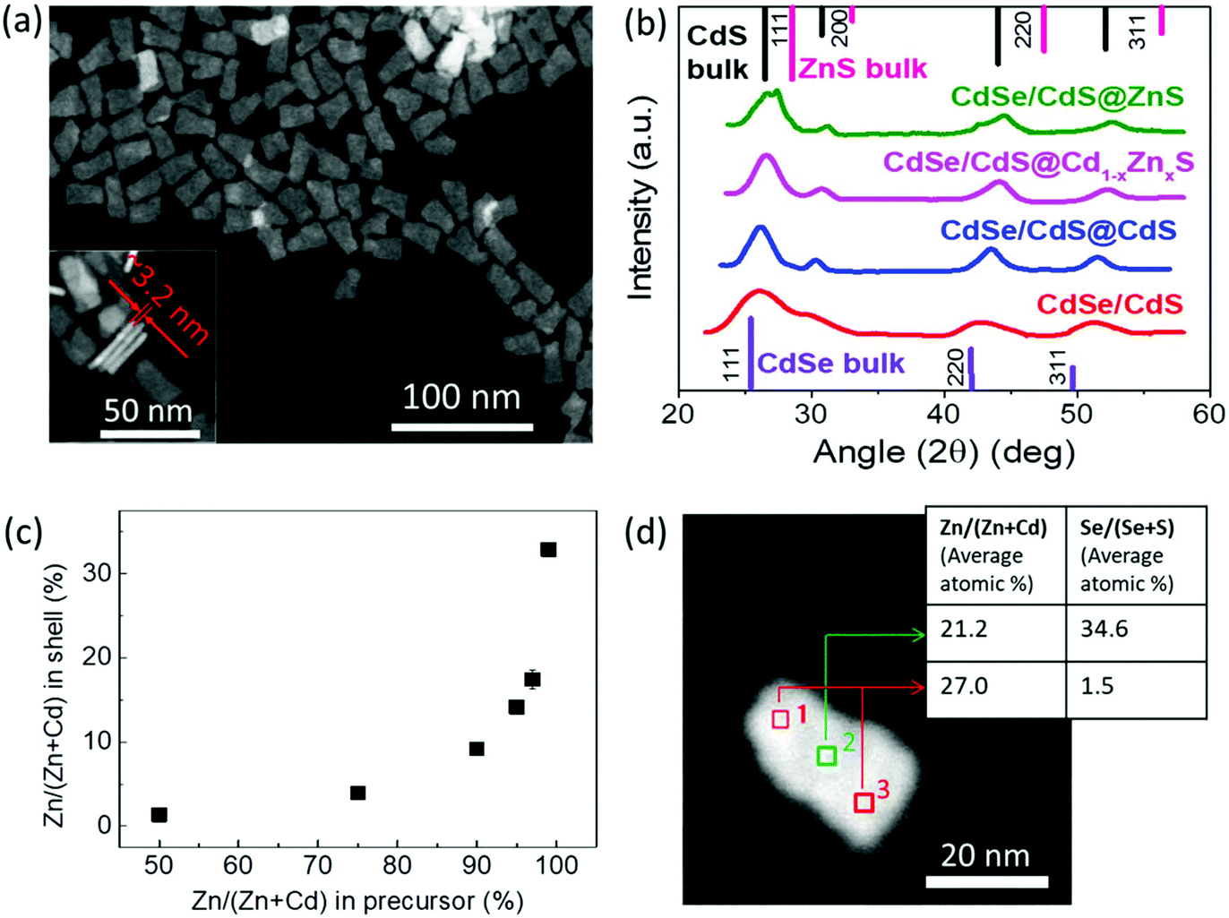 | ||
| Fig. 2 Structural characterization of the NPLs. (a) A HAADF-TEM image of core/crown@shell NPLs. Inset to (a) shows the thickness of core/crown@shell NPLs with 6 MLs of Cd1−xZnxS shells in the gradient alloy composition is ≈3.2 ± 0.3 nm. (b) XRD spectrum of core/crown and different core/crown@shell NPLs. (c) ICP-MS results showing the percentage of Zn incorporated into the shells at various amounts of Zn in the precursor solutions used for the shell growth. (d) Average atomic percentage of elements measured via TEM-EDX spectroscopy at different locations on single core/crown@shell NPLs with 6 MLs of Cd1−xZnxS. | ||
To understand the correlation between the Zn:Cd ratio in the precursor and the actual Zn content incorporated into the shell layers, we performed inductively coupled plasma mass spectrometry (ICP-MS) on samples prepared with precursor solutions having different ratios of Zn:Cd. Fig. 2(c) shows the relationship between the Zn/(Zn + Cd) percentage in the precursor mixture with the actual Zn/(Zn + Cd) percentage content in the shell calculated using ICP-MS measurements. The percentage of Zn incorporated into the shell increases in a nonlinear fashion compared to the increase of Zn content in the precursor mixture. For example, while a precursor solution containing equal amounts of Zn and Cd precursors in NMF resulted in only ∼2% of Zn/(Zn + Cd) content in the shell, another precursor solution having a ratio of 99:1 Zn:Cd led to ∼35% Zn content in the shell. This might be attributed to the higher reactivity of the Cd precursor compared to the Zn precursor at room temperature and/or to the lattice matching induced favorable growth of the CdS shell over ZnS.40 As can be seen in Fig. 2(c), for the incorporation of only 10% of Zn to the shell, the precursor mixture should contain at least 90% of Zn. In our trials, we observed a high PL QY in the core/crown@shell samples with shells synthesized using precursors containing greater than 90% Zn. For instance, for the gradient alloy samples presented in Table 1, the Zn content in the precursor mixtures for 2, 4, 6 and 8 ML shells was 93, 97, 99 and 100%, respectively. Thus, the Zn content was engineered to gradually increase from around <20% in the first shell to a purely ZnS shell in the outermost layer to obtain a gradient shell composition resulting in relaxed lattice strain that produces a high PL QY while retaining the narrow emission. The energy dispersive X-ray spectroscopy (EDX) measurement performed at different locations on a single NPL using TEM also confirms a similar atomic content of the cationic elements (shown in Fig. 2(d)) and reflects the core/crown@shell geometry with the NPL center showing a large Se concentration while the NPL edge consists of almost entirely S anions.
The CdSe/CdS@Cd1−xZnxS core/crown@shell NPL sample having 6 MLs of the Cd1−xZnxS gradient alloy shell and exhibiting a QY of ∼50% in NMF was further dispersed in aqueous and non-polar media by using different ligands for the surface passivation. The NPLs were dispersed in hexane or toluene by adding oleylamine and stirring overnight, after which the PL QY of the sample increased to 70–75%. To disperse these NPLs into water, ethylenediamine (EDA) assisted ligand exchange41 with 3-mercaptopropionic acid (MPA) was performed on the NPLs in toluene. The process of this ligand exchange is described in detail in the ESI.† To compensate for any surface etching,41 a small quantity of zinc nitrate dissolved in water was added and the NPL solution was stirred overnight under room light. The PL and absorbance spectra of these NPLs in different solvents are shown in Fig. 3(a). NPLs have a PL peak at 618 nm with a fwhm of ∼66 meV in NMF. After transferring the NPLs from NMF to toluene, the peak of their PL emission blue-shifted to 616 nm and further shifted to 614 nm when transferred to water but the fwhm of ∼68–70 meV was retained. This PL shift was possibly due to the surface etching of NPLs during the ligand exchange in water. However, by adding some zinc nitrate during ligand exchange as mentioned earlier, we minimized the possible damage to the surface. Immediately after the ligand exchange, the PL QY of NPLs in water was about 70–80%, depending on the concentration of MPA used for the ligand exchange.41 An enhancement in PL QY after the ligand exchange with thiolated ligands has also been observed before which was found to depend on the bandgap energy of the used QDs and was speculated to arise from stronger binding and more compact capping density of thiolated ligands in comparison to bulkier original aliphatic ligands.41 However, more systematic experiments are required to definitively attribute the exact causes of PL enhancement after ligand exchange, especially while taking note of the different surface-curvatures in QDs and NPLs. We further observed the photo-enhancement of the PL QY up to 85–90% for the MPA passivated aqueous samples under ambient light illumination over many days (15–20 days). Under optimum conditions, these samples remained stable with a QY >80% in the water solution for nearly 6 months. A similar illumination-assisted increase in PL QY was observed previously associated with different photoactivation mechanisms, for example light-induced ligand rearrangement and photo-oxidation of the nanocrystal surface accompanied by the photoadsorption of water molecules on the surface leading to defect passivation.42 Our aqueous NPL samples were handled under an ambient atmosphere, thus the photobrightening occurred in the presence of oxygen. However, the exact mechanism of the photoenhancement needs to be studied further. We also performed EDA-assisted ligand exchange using other thiolated ligands like thioglycolic acid (TGA) and 11-mercaptoundecanoic acid (MUA). For us, the PL QY enhancement with TGA and MPA (80–90%) was better than that with MUA (60–70%). We also observed that the MUA-coated sample underwent agglomeration and became gelatinous-cloudy after a few days (ESI, Fig. S20†) which could possibly have caused a lower PL QY. Thus, we obtained gradient alloy shell NPLs in water having an fwhm of ∼68 meV accompanied by a high PL QY reaching up to 90%. The PL QYs were measured in an integrating sphere as a ratio of the absolute number of emitted photons to absorbed photons with excitation at 400 nm and also using Rh101 dye43 as a reference excitation at 490–500 nm. Also, all the reactions were carried out in air, which shows that these NPLs are air-stable.
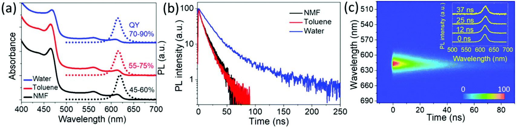 | ||
| Fig. 3 Steady-state and time-resolved PL measurements of the NPLs in different solvents. (a) Absorbance and PL spectra of the 6 ML gradient alloy shell sample in different solvents, (b) time-resolved PL measurement for the NPLs in different solvents and (c) a time–wavelength dependence of PL intensity of NPLs dispersed in water following excitation at 400 nm (1 kHz, 150 fs, 0.5 μJ cm−2). Inset of (c) shows the transient PL spectra at different times. | ||
Fig. 3(b) shows time-resolved PL (TRPL) measurements performed on the NPLs with 6 ML gradient alloy shells in different solvents using a streak camera having a temporal resolution of ∼10 ps and 400 nm excitation (repetition rate: 1 kHz, pulse width: 150 fs). We fitted the PL decay for the water–NPL samples with a bi-exponential decay function, yielding lifetimes of τ1 ∼17 ns and τ2 ∼77 ns. The NMF and toluene based samples were best fit with tri-exponential decay functions. Both the solutions have all lifetime components in similar ranges, specifically τ1 ∼1–2 ns, τ2 ∼7–8 ns and τ3 ∼18–19 ns. The fit parameters are shown in Table S1 in the ESI.† The intensity-weighted lifetimes given by (∑Aτ2/∑Aτ) for toluene and NMF are in the range of 11–13 ns, whereas for water solution, it is 35 ns, indicating a ∼3-fold increase in the lifetime of the NPLs in water. This can be attributed to the improved surface passivation which results in a superior PL QY and the difference between the dielectric constants of the solvent media. In Fig. 3(c), the pseudo-color TRPL plot from the streak camera measurement on a shorter time scale (with a higher resolution) for the aqueous sample is shown. Transient PL spectra at different time instances at 0 ns, 12 ns, 25 ns, and 37 ns after the laser excitation pulse shows a negligible red shift (<2 nm) of PL peak position, an insignificant change in fwhm and identical TRPL decays at different emission positions (ESI, Fig. S6†), indicating the type-I band alignment of the transition.44,45
Developing water-based high PL QY NPLs opens the pathway to using them in biological and optoelectronic applications. With a narrow fwhm, multiple NPLs emitting in pure colors can be used in a signal multiplexed fashion for cell imaging. Also, their hydrophilicity can be exploited to achieve controlled assemblies and functional architectures.46 To this end, we successfully achieved the patterned deposition of our NPLs on a glass substrate using poly(diallyldimethylammoniumchloride) (PDDA) linker molecules. Fig. 4(a) shows the mapping of the PL intensity of the water-based NPLs attached onto electron beam lithography (EBL) patterned glass substrates, captured using a confocal imaging microscope with 375 nm excitation. This process is similar to the layer-by-layer assembly techniques reported earlier.47 Briefly, a glass substrate coated with poly(methyl methacrylate) (PMMA) was patterned with EBL and the surface of the substrate without PMMA was made hydrophilic by O2-plasma treatment applied at low power. The substrates were then dipped into a PDDA linker solution for the attachment of linker molecules onto the exposed areas followed by dipping into aqueous NPL solution to attach the MPA functionalized NPLs on top of the linker molecules.
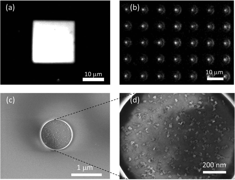 | ||
| Fig. 4 SEM images and PL intensity maps of the attached NPLs. A PL intensity map of NPLs from (a) a ∼20 × 20 μm2 square pattern and (b) a pattern with holes having 1 μm diameter. Here the intensity images are captured using a confocal microscope. In (b), circular rings due to the diffraction of the emitted light from the 1 μm diameter holes can be seen. (c) An SEM image of one of the 1 μm diameter holes showing NPLs attached on the surface in the patterned area. (d) A zoomed-in SEM image for one such 1 μm diameter hole to clearly see the NPL attachment in the patterned area. | ||
The PL intensity image captured with a confocal microscope from a square pattern having a size of ∼20 × 20 μm2 attached with CdSe/CdS@Cd1−xZnxS NPLs emitting at ∼620 nm is presented in Fig. 4(a). As can be seen from the PL intensity map, the coverage of NPLs on the EBL patterned area is uniform, even retained at the sharp edges of the square. In Fig. 4(b), the PL intensity mapping collected from an array of circular dots with a diameter of 1 μm is presented. In this image, the emitted light from the NPLs is diffracted at the edges of the patterned holes to form circular rings since the size of patterned holes is close to the emission wavelength. A scanning electron microscope (SEM) image for the circular dot patterns is shown in Fig. 4(c), while a further close-up image of the same pattern shows the NPLs attached inside the patterned area. As illustrated in ESI, Fig. S7 and S8,† this technique can be used to obtain assemblies of NPLs even for just single-layer deposition on patterns of any shape having a size as small as a few hundreds of nanometers, which is significantly smaller than the previously demonstrated QD deposited patterns having sizes from tens to hundreds of micrometers obtained by photolithography.46,47 The flat planar geometry of these 2D NPLs with a large surface area makes their attachment robust and favorable compared to spherical QDs usually having sizes of a few nanometers. By using multiple layers of deposition in a pixelated fashion, this attachment technique could be put to good use to make large-area displays avoiding the wastage of materials (for example, in micro-LEDs), unlike spin-coating deposition of solution-processed nanocrystals suffering high wastage.
Typically NPL films have been observed to exhibit high prevalence of stacking, which leads to the loss of efficiency via fast nonradiative exciton transfer and exciton sinking in defected sub-populations, and undermines their uniform film formation and hence the performance of the obtained devices.48,49 Controlled film formation is significantly important for NPLs suffering from stacking. Partial stacking of our hetero-NPLs on the TEM grid obtained by drop-casting from a hexane solution also can be seen in the STEM images shown in ESI, Fig. S9(a).† However, as can be observed from the SEM images (Fig. 4b and ESI, Fig. S9(b)†), uniform deposition on the flat surface of the NPLs devoid of any stacking can be achieved robustly using the attachment technique with aqueous NPLs through a linker. Our method using the attachment through linkers provides a novel pathway for such aqueous NPLs to form non-stacked films and achieve controllably oriented assemblies of these NPLs, which is also important in elucidating the optical processes in the NPLs hindered by their different orientations within the ensemble.
Obtaining controlled assemblies of NPLs is highly advantageous for optoelectronics, thanks to their directional emission emanating from their anisotropic 2D electronic structure.50,51 In NPLs, the band-edge emission associated with the heavy hole transition occurs predominantly in the direction perpendicular to the NPL surface due to the highly anisotropic heavy hole exciton transition dipole distribution lying within the NPL plane.50,51 Thus having an assembly of NPLs with their flat surfaces, the so-called bright planes oriented in the same direction should give rise to directional emission perpendicular to the surface of the deposited assembly layer. Such a controlled orientation of the emission dipole in NPLs can be obtained using techniques such as interfacial assembly51 and stretching.52 We performed back focal plane (k-space) imaging to investigate the directionality of the emission of our aqueous core/crown@shell NPLs attached on a glass substrate using the linker method. A schematic representation of the obtained films of the NPLs attached with the linker is given in Fig. 5(a), along with those of the red-emitting QDs (having intrinsically isotropic emission) spin-coated from a toluene solution and the core/crown@shell NPLs spin-coated from a toluene solution on glass substrates for the emission directivity measurements. The details of the experimental setup are provided in the ESI.† Briefly, an oil immersed objective lens with a numerical aperture (NA) of 1.25 was used to excite the samples and collect the emission via the glass substrate. The pseudo-momentum space (k) is related to the elevation angle of emission θ of the NPLs by the formula: k = nsin(θ), where n is the refractive index of the immersion oil (1.52 in this case). The maximum collection k = 1.25 (θ = 55.3°) was limited by the NA of the objective lens. Fig. 5(b) and (c) show the k-dependent and θ-dependent intensity profile of the p-polarized emission from the prepared samples, respectively. The θ-dependent intensity profile presented in the polar plot was obtained by performing Jacobian conversion on the k-dependent emission profile.53 The dip around the kx/k0 = 1 value in Fig. 5(b), corresponding to the total internal reflection angle at the air interface, for the NPL-attached sample is ∼52% deeper compared to the reference QD and NPL spin-coated samples (which are nearly similar to each other). This indicates a lower fraction of out-of-plane oriented transition dipoles in the NPL-attached sample.50 Using a theoretical model50,54 to fit the k-dependent emission profile of the NPL-attached sample, we obtain a value of 91% for the contribution from in-plane dipole transitions (see ESI, Fig. S19†). Correspondingly, the angle-dependent intensity profile from the polar plots (Fig. 5(c)) shows a more prolate shape compared to the other two samples, indicating a more directed emission from the NPL-attached sample. The spin-coated NPL film exhibits an emission profile similar to the QD film indicating a nearly isotropic emission. This can be explained by the presence of randomly oriented and partially stacked NPLs as depicted in Fig. 5(a). Such directed emission from NPLs with an anisotropic 2D electronic structure is highly advantageous to reduce the coupling of emitted energy to surface plasmon modes of the electrodes in LEDs55 and the loss of energy in waveguide modes.55–57 Therefore, such an assembly technique provides the potential to enhance the outcoupling efficiency of LEDs in displays and lighting.50,58
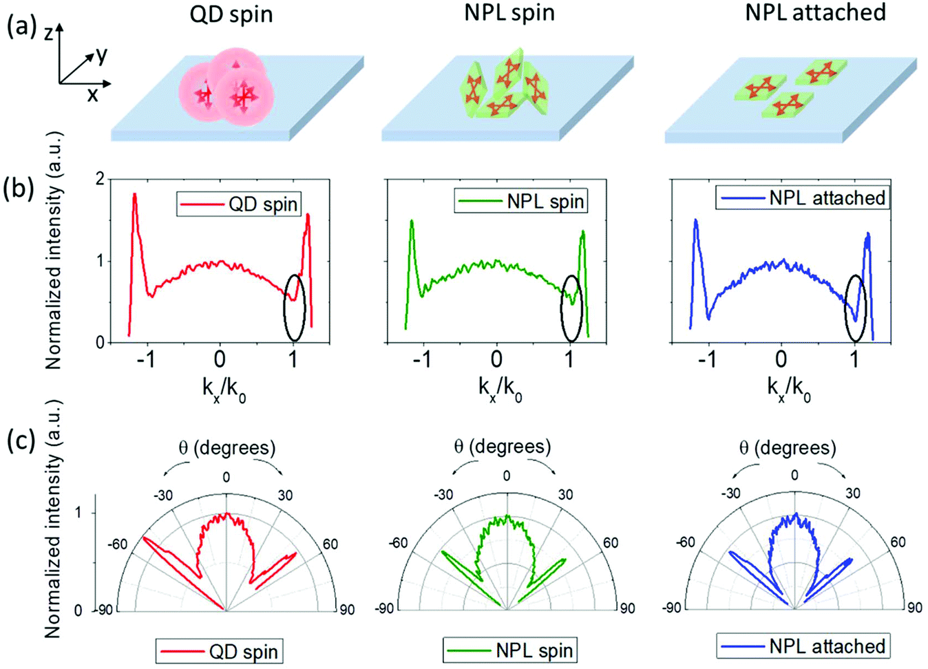 | ||
| Fig. 5 Angle and k-space dependent p-polarized emission characteristics of spin-coated spherical QDs, spin-coated NPLs, and attached NPLs. (a) A schematic representation of the film of spin-coated QDs, spin-coated NPLs and NPLs via linker-based attachment on glass substrates. (b) k-Dependent and (c) θ-dependent intensity profile of p-polarized spectra of all samples. k0 is the wavevector in air. Angle-dependent polar plots were obtained by performing Jacobian conversion on the k-space spectra. The substrate is on the x–y plane. The plane of incidence for the emitted light is on the x–z plane. The collected radiation emitted in the x–z plane (defined as p-polarized) emanates from a distribution of emitter dipoles oriented in-plane (px) and out-of-plane (pz) of the substrate. | ||
Conclusion
In conclusion, we have demonstrated the synthesis of CdSe/CdS@Cd1−xZnxS core/crown@shell NPLs having a type-I band alignment with shells in gradient alloy composition not only preserving the high efficiency of the core/crown seeds but also enhancing their photostability by confining the excitons and isolating them from the surface. Our controlled shell growth with a monolayer precision at a targeted alloy composition allowed us to precisely tune the optimum shell composition and hence strain and confinement at the monolayer level for potentially maximizing the PL QY. Aqueous dispersions of these NPLs were achieved by ligand replacement via MPA reaching quantum yields up to 90%. The significantly long PL lifetime (∼35 ns) of the NPLs dispersed in water results from the effective passivation of nonradiative recombination channels, while being accompanied by a high PL QY. We also demonstrated the precisely controlled attachment and film formation of our NPLs on the nanoscale for the first time by exploiting their hydrophilicity and 2D geometry. We believe that this may be significantly important for achieving high-efficiency optoelectronic devices based on 2D colloidal NPLs, which otherwise suffer from nonuniform film formation because of the strong stacking phenomena taking place in these 2D structures. We show that such controlled attachment can also be used to obtain directional emission from these NPLs when compared to their films formed by conventional spin-casting techniques. Thus, the attachment approach provides a novel route to improve light extraction and outcoupling efficiency. With their very high QYs, narrow emission and controlled film formation exhibiting a highly directed emission, aqueous CdSe/CdS@Cd1−xZnxS core/crown@shell NPLs present a unique platform possibly for biological and optoelectronic applications, especially for biolabelling, lasing and LEDs.Author contributions
H. V. D. and S. D. conceived the idea of this project and H. V. D. supervised the research work. S. S. and S. D. synthesized the materials and performed the NPL attachment. S. S. carried out confocal PL measurements. M. L. performed the time-resolved PL measurements. M. L., T. C. S. and S. S. analysed the time-resolved PL measurements. D. D. performed TEM, XRD, and ICP-MS measurements. O. E. performed SEM measurements. Z. P. fabricated EBL patterned substrates. S. T. H., Y. H. F. and A. I. K. performed and analysed the back-focal plane microscopy measurements. P. L. H. M., J. Y. and C. D. carried out the theoretical modelling. H. V. D., S. S. and S. D. wrote the manuscript. All authors discussed the results and commented on the manuscript.Conflicts of interest
There are no conflicts to declare.Acknowledgements
This research is supported by the National Research Foundation, Prime Minister's Office, Singapore under its NRF Investigatorship Award program (NRF-NRFI2016-08) and the Singapore Agency for Science, Technology and Research (A*STAR) SERC Pharos Program under Grant No. 152 73 00025. T. C. S. acknowledges the funding support from the Ministry of Education (MOE) Tier 1 grant RG 173/16, and MOE Tier 2 grants MOE2015-T2-2-015 and MOE2016-T2-1-034, and from the Singapore National Research Foundation through the Competitive Research Programme NRF-CRP14-2014-03. C. D. would like to acknowledge the financial support from the Singapore Ministry of Education AcRF Tier-1 grant (MOE-RG178/17). The authors acknowledge Vytautas Valuckas (IMRE, A*STAR) for his help with SEM imaging of the attached nanoplatelets.References
- D. V. Talapin, J.-S. Lee, M. V. Kovalenko and E. V. Shevchenko, Chem. Rev., 2010, 110, 389–458 CrossRef CAS PubMed.
- M. V. Kovalenko, L. Manna, A. Cabot, Z. Hens, D. V. Talapin, C. R. Kagan, V. I. Klimov, A. L. Rogach, P. Reiss, D. J. Milliron, P. Guyot-Sionnnest, G. Konstantatos, W. J. Parak, T. Hyeon, B. A. Korgel, C. B. Murray and W. Heiss, ACS Nano, 2015, 9, 1012–1057 CrossRef CAS PubMed.
- T. Erdem and H. V. Demir, Nanophotonics, 2016, 5, 22 Search PubMed.
- J. Owen and L. Brus, J. Am. Chem. Soc., 2017, 139, 10939–10943 CrossRef CAS PubMed.
- U. Resch-Genger, M. Grabolle, S. Cavaliere-Jaricot, R. Nitschke and T. Nann, Nat. Methods, 2008, 5, 763–775 CrossRef CAS PubMed.
- D. R. Larson, W. R. Zipfel, R. M. Williams, S. W. Clark, M. P. Bruchez, F. W. Wise and W. W. Webb, Science, 2003, 300, 1434–1436 CrossRef CAS PubMed.
- M. Bruchez, M. Moronne, P. Gin, S. Weiss and A. P. Alivisatos, Science, 1998, 281, 2013–2016 CrossRef CAS PubMed.
- L. Gurinovich, M. Artem'ev, A. Lyutich and S. Gaponenko, J. Appl. Spectrosc., 2006, 73, 572–575 CrossRef CAS.
- V. Lesnyak, N. Gaponik and A. Eychmüller, Chem. Soc. Rev., 2013, 42, 2905–2929 RSC.
- L. Jing, S. V. Kershaw, Y. Li, X. Huang, Y. Li, A. L. Rogach and M. Gao, Chem. Rev., 2016, 116, 10623–10730 CrossRef CAS PubMed.
- H. Bao, Y. Gong, Z. Li and M. Gao, Chem. Mater., 2004, 16, 3853–3859 CrossRef CAS.
- Y. He, L.-M. Sai, H.-T. Lu, M. Hu, W.-Y. Lai, Q.-L. Fan, L.-H. Wang and W. Huang, Chem. Mater., 2007, 19, 359–365 CrossRef CAS.
- S. F. Wuister, C. de Mello Donega and A. Meijerink, J. Phys. Chem. B, 2004, 108, 17393–17397 CrossRef CAS.
- O. Chen, J. Zhao, V. P. Chauhan, J. Cui, C. Wong, D. K. Harris, H. Wei, H.-S. Han, D. Fukumura and R. K. Jain, Nat. Mater., 2013, 12, 445–451 CrossRef CAS PubMed.
- F. Di Stasio, J. Q. Grim, V. Lesnyak, P. Rastogi, L. Manna, I. Moreels and R. Krahne, Small, 2015, 11, 1328–1334 CrossRef CAS PubMed.
- F. Lübkemann, R. Anselmann, T. Kodanek and N. C. Bigall, Chem. Ing. Tech., 2017, 89, 807–813 CrossRef.
- S. J. Lim, D. R. McDougle, M. U. Zahid, L. Ma, A. Das and A. M. Smith, J. Am. Chem. Soc., 2016, 138, 64–67 CrossRef CAS PubMed.
- M. Nasilowski, B. Mahler, E. Lhuillier, S. Ithurria and B. Dubertret, Chem. Rev., 2016, 116, 10934–10982 CrossRef CAS PubMed.
- M. Olutas, B. Guzelturk, Y. Kelestemur, A. Yeltik, S. Delikanli and H. V. Demir, ACS Nano, 2015, 9, 5041–5050 CrossRef CAS PubMed.
- M. D. Tessier, C. Javaux, I. Maksimovic, V. Loriette and B. Dubertret, ACS Nano, 2012, 6, 6751–6758 CrossRef CAS PubMed.
- M. I. D. Tessier, P. Spinicelli, D. Dupont, G. Patriarche, S. Ithurria and B. Dubertret, Nano Lett., 2014, 14, 207–213 CrossRef CAS PubMed.
- S. Ithurria and D. V. Talapin, J. Am. Chem. Soc., 2012, 134, 18585–18590 CrossRef CAS PubMed.
- S. Delikanli, M. Z. Akgul, J. R. Murphy, B. Barman, Y. Tsai, T. Scrace, P. Zhang, B. Bozok, P. L. Hernández-Martínez and J. Christodoulides, ACS Nano, 2015, 9, 12473–12479 CrossRef CAS PubMed.
- S. Delikanli, B. Guzelturk, P. L. Hernández-Martínez, T. Erdem, Y. Kelestemur, M. Olutas, M. Z. Akgul and H. V. Demir, Adv. Funct. Mater., 2015, 25, 4282–4289 CrossRef CAS.
- Y. Kelestemur, B. Guzelturk, O. Erdem, M. Olutas, K. Gungor and H. V. Demir, Adv. Funct. Mater., 2016, 26, 3570–3579 CrossRef CAS.
- B. Mahler, B. Nadal, C. Bouet, G. Patriarche and B. Dubertret, J. Am. Chem. Soc., 2012, 134, 18591–18598 CrossRef CAS PubMed.
- A. A. Rossinelli, A. Riedinger, P. Marqués-Gallego, P. N. Knüsel, F. V. Antolinez and D. J. Norris, Chem. Commun., 2017, 53, 9938–9941 RSC.
- A. Polovitsyn, Z. Dang, J. L. Movilla, B. Martin-Garcia, A. H. Khan, G. H. Bertrand, R. Brescia and I. Moreels, Chem. Mater., 2017, 29, 5671–5680 CrossRef CAS.
- M. Tessier, B. Mahler, B. Nadal, H. Heuclin, S. Pedetti and B. Dubertret, Nano Lett., 2013, 13, 3321–3328 CrossRef CAS PubMed.
- Y. Kelestemur, M. Olutas, S. Delikanli, B. Guzelturk, M. Z. Akgul and H. V. Demir, J. Phys. Chem. C, 2015, 119, 2177–2185 CrossRef CAS.
- B. Guzelturk, Y. Kelestemur, M. Olutas, S. Delikanli and H. V. Demir, ACS Nano, 2014, 8, 6599–6605 CrossRef CAS PubMed.
- T. Kodanek, H. M. Banbela, S. Naskar, P. Adel, N. C. Bigall and D. Dorfs, Nanoscale, 2015, 7, 19300–19309 RSC.
- D. V. Talapin, A. L. Rogach, I. Mekis, S. Haubold, A. Kornowski, M. Haase and H. Weller, Colloids Surf., A, 2002, 202, 145–154 CrossRef CAS.
- C.-T. Cheng, C.-Y. Chen, C.-W. Lai, W.-H. Liu, S.-C. Pu, P.-T. Chou, Y.-H. Chou and H.-T. Chiu, J. Mater. Chem., 2005, 15, 3409–3414 RSC.
- R. Xie, U. Kolb, J. Li, T. Basché and A. Mews, J. Am. Chem. Soc., 2005, 127, 7480–7488 CrossRef CAS PubMed.
- G. E. Cragg and A. L. Efros, Nano Lett., 2010, 10, 313–317 CrossRef CAS PubMed.
- W. K. Bae, L. A. Padilha, Y.-S. Park, H. McDaniel, I. Robel, J. M. Pietryga and V. I. Klimov, ACS Nano, 2013, 7, 3411–3419 CrossRef CAS PubMed.
- D. V. Talapin, I. Mekis, S. Götzinger, A. Kornowski, O. Benson and H. Weller, J. Phys. Chem. B, 2004, 108, 18826–18831 CrossRef CAS.
- W. K. Bae, K. Char, H. Hur and S. Lee, Chem. Mater., 2008, 20, 531–539 CrossRef CAS.
- L. Manna, E. C. Scher, L.-S. Li and A. P. Alivisatos, J. Am. Chem. Soc., 2002, 124, 7136–7145 CrossRef CAS PubMed.
- M.-Q. Dai and L.-Y. L. Yung, Chem. Mater., 2013, 25, 2193–2201 CrossRef CAS.
- C. Carrillo-Carrión, S. Cárdenas, B. M. Simonet and M. Valcárcel, Chem. Commun., 2009, 5214–5226 RSC.
- T. Karstens and K. Kobs, J. Phys. Chem., 1980, 84, 1871–1872 CrossRef CAS.
- J. He, C. Reyner, B. Liang, K. Nunna, D. Huffaker, N. Pavarelli, K. Gradkowski, T. Ochalski, G. Huyet and V. Dorogan, Nano Lett., 2010, 10, 3052–3056 CrossRef CAS PubMed.
- Y. Gao, M. Li, S. Delikanli, H. Zheng, B. Liu, C. Dang, T. C. Sum and H. V. Demir, Nanoscale, 2018, 10, 9466–9475 RSC.
- J.-S. Park, J. Kyhm, H. H. Kim, S. Jeong, J. Kang, S.-E. Lee, K.-T. Lee, K. Park, N. Barange and J. Han, Nano Lett., 2016, 16, 6946–6953 CrossRef CAS PubMed.
- Y. W. Lin, W. L. Tseng and H. T. Chang, Adv. Mater., 2006, 18, 1381–1386 CrossRef CAS.
- O. Erdem, M. Olutas, B. Guzelturk, Y. Kelestemur and H. V. Demir, J. Phys. Chem. Lett., 2016, 7, 548–554 CrossRef CAS PubMed.
- B. Guzelturk, O. Erdem, M. Olutas, Y. Kelestemur and H. V. Demir, ACS Nano, 2014, 8, 12524–12533 CrossRef CAS PubMed.
- R. Scott, J. Heckmann, A. V. Prudnikau, A. Antanovich, A. Mikhailov, N. Owschimikow, M. Artemyev, J. I. Climente, U. Woggon and N. B. Grosse, Nat. Nanotechnol., 2017, 12, 1155–1160 CrossRef CAS PubMed.
- Y. Gao, M. C. Weidman and W. A. Tisdale, Nano Lett., 2017, 17, 3837–3843 CrossRef CAS PubMed.
- P. D. Cunningham, J. O. B. Souza Jr., I. Fedin, C. She, B. Lee and D. V. Talapin, ACS Nano, 2016, 10, 5769–5781 CrossRef CAS PubMed.
- J. Mooney and P. Kambhampati, J. Phys. Chem. Lett., 2013, 4, 3316–3318 CrossRef CAS.
- J. A. Schuller, S. Karaveli, T. Schiros, K. He, S. Yang, I. Kymissis, J. Shan and R. Zia, Nat. Nanotechnol., 2013, 8, 271 CrossRef CAS PubMed.
- J. Frischeisen, D. Yokoyama, A. Endo, C. Adachi and W. Brütting, Org. Electron., 2011, 12, 809–817 CrossRef CAS.
- X. Chen, C. Ji, Y. Xiang, X. Kang, B. Shen and T. Yu, Opt. Express, 2016, 24, A935–A942 CrossRef CAS PubMed.
- D. Y. Kim, J. H. Park, J. W. Lee, S. Hwang, S. J. Oh, J. Kim, C. Sone, E. F. Schubert and J. K. Kim, Light: Sci. Appl., 2015, 4, e263 CrossRef CAS.
- W. Brütting, J. Frischeisen, T. D. Schmidt, B. J. Scholz and C. Mayr, Phys. Status Solidi A, 2013, 210, 44–65 CrossRef.
Footnote |
| † Electronic supplementary information (ESI) available: Details of synthesis procedures, experimental set-up, theoretical modelling and additional figures. See DOI: 10.1039/c8nr07879c |
| This journal is © The Royal Society of Chemistry 2019 |