
 Open Access Article
 This Open Access Article is licensed under a Creative Commons Attribution-Non Commercial 3.0 Unported Licence
Flexible focusing pattern realization of centimeter-scale planar super-oscillatory lenses in parallel fabrication†
Wenli
Li
 ab,
Yiting
Yu
*ab and
Weizheng
Yuan
*ab
ab,
Yiting
Yu
*ab and
Weizheng
Yuan
*ab
aKey Laboratory of Micro/Nano Systems for Aerospace (Ministry of Education), Northwestern Polytechnical University, Xi'an 710072, China. E-mail: yyt@nwpu.edu.cn
bShaanxi Province Key Laboratory of Micro and Nano Electro-Mechanical Systems, Northwestern Polytechnical University, Xi'an 710072, China. E-mail: yuanwz@nwpu.edu.cn
First published on 11th December 2018
Abstract
Planar super-oscillatory lenses (SOLs) can exert far-field foci beyond the diffraction limit free from the contribution of evanescent waves. However, the reported design methods of SOLs are always complicated and divergent, leading to a poor control over the desired focusing patterns. Furthermore, the existing device sizes of SOLs are mainly within hundreds of micrometers accompanied by a subwavelength-scale feature size. Here, we propose a general optimization design model for realizing flexible focusing patterns, e.g. multifocal and achromatic contours. Additionally, a novel design called the chromatic-customized SOL fighting against the dispersion rule of traditional diffractive optical elements (DOEs) is also demonstrated based on the proposed flexible algorithm. The diameters for all the SOLs reach 12 mm with 30 μm minimum feature size, which can be easily fabricated by employing the conventional optical lithography technique. Such centimeter-scale, light weight and low-cost lenses reveal new capacities of arbitrarily customized optical patterns in various interdisciplinary fields including parallel particle trapping, full-color high-resolution imaging, and compact spectral imaging.
Introduction
The conventional optical lenses are subjected to two major challenges, i.e. resolution limit and chromatic aberration. Moreover, the inevitably bulky form makes them hard to integrate, resulting in ever-growing efforts to develop omnifarious planar lenses. Superlenses1 and plasmonic lenses2,3 have been studied for more than twenty years as two kinds of planar lenses, in which surface plasmons behaving as a kind of evanescent wave were manipulated to realize super-resolution in the near field, mainly for applications in super-resolution imaging4–6 and nanolithography.7 However, the evanescent waves attenuate exponentially due to the energy loss in the medium and cannot propagate to the far field or even the quasi-far field, imposing a fatal limit for practical uses. Recently, metalenses constructed as optical metasurfaces, which are two-dimensional configurations of metamaterials of ultrathin thickness, have caused considerable concerns since they can control light propagation in a desirable manner and achieve foci close to the diffraction limit, providing a feasible route to develop planar optical devices.8–12 Owing to the subwavelength-scale unit cell, the device sizes for this kind of planar lens can be fabricated with difficulty to the centimeter scale suitable for visible light.On the other hand, a non-invasive optical far-field focusing and imaging technique based on super-oscillatory lenses (SOLs) was also proposed.13–16 The optical super-oscillation phenomenon is the delicate interference of far-field propagating waves carrying the fine physical details of objects, and it can be accurately engineered to achieve sub-diffraction-limit foci, even smaller than the size defined as the super-oscillatory criterion 0.38λ/NA (where NA is the numerical aperture).17,18 However, the peak-intensity ratio between the strongest side-lobe and central main-lobe is 16.2% for super-oscillation hotspots, and the focal spot can be further reduced with the exponentially increasing side-lobe intensity.19 Consequently, the small super-oscillation hotspots are always accompanied by the inevitably moderate side lobes, bringing a certain inconvenience for practical applications, especially in the field where it doesn't need a too small hotspot but a wide enough effective field of view for optical imaging. To make a reasonable balance among centimeter-scale lens, the subwavelength hotspot, extremely long working distance and relative weak side lobes for practical applications, we confined the hotspots within the range between the super-oscillatory criterion and the Rayleigh criterion20 to customize the centimeter-scale planar super-resolution lens with an extremely long working distance.
In the previous binary SOL-based super-focusing work, SOLs were optimized by means of the genetic algorithm (GA)13,21 or binary particle swarm optimization (BPSO) algorithm,16,22 for which complicated approaches were required to construct super-oscillatory light fields, however with low-efficiency control. In our previous work, we proposed the multi-objective and multi-constraint optimization method to acquire super-focusing light fields with patterns of optical needle23 or multi-foci.24 However, the demonstrated method needs a large number of initial populations to launch the iterative process and shows a poor convergence. To develop a highly efficient and controllable iterative procedure, we are here aiming to substitute the constraints as penalty functions into GA combined with the vectorial angular spectrum (VAS) theory. Consequently, the existing multi-objective and multi-constraint problem is transformed to an unconstrained multi-objective optimization issue which can easily meet various design requirements, solving the problems of divergence and low efficiency.
Restrictions in the design complexity and bulky form for the traditional diffractive multifocal and achromatic lenses are inevitable.25–28 We handle these two optical patterns that can be arbitrarily achieved through a single SOL. In practice, the far-field super-resolution multifocal lens and achromatic lens can find their various opportunities in parallel particle trapping, three-dimensional data storage and full-color high-resolution imaging. It's worth mentioning that the achromatic design of SOL was made possible through creating different foci of long depths and making them partially overlap to focus at the same point.29 Nevertheless, it could not be treated as a direct way to realize the achromatic optical contour, and a much more controllable design is urgently needed. In addition, the proposed optimization algorithm can be applied to exploit an achromatic-customized optical field which manifests noticeable contradiction to the dispersive rule of traditional diffractive optical elements (DOEs), namely a longer wavelength brings about a shorter focal length. Based on our novel design idea, an achromatic-customized SOL can be realized at will to develop its promising applications in compact diffractive spectral imaging systems and portable spectrometers.
The other key factor that influences the practical applications of planar SOLs is the fabrication process. To make a general survey on the fabrication technologies for the reported SOLs,13,22,30–38 as shown in Fig. 1, most devices were fabricated by focused ion beam (FIB) milling or electron beam lithography (EBL) because of their deep-subwavelength fabrication capability. Owing to the characteristics of high cost, time consumption, and specific material requirements, these two common fabrication methods cannot be the first choice to prepare devices on a large scale. Notably, parallel fabrication of planar SOLs is becoming the main trend. Recently, a SOL with a 1.2 μm line width was first proposed19 instead of the subwavelength-scale feature size. However, the diameter of the reported device fabricated by deep ultra-violet (DUV) lithography was just 600 μm bringing a big difficulty in integrating with the existing centimeter-scale optical systems. More recently, direct laser writing (DLW) lithography was employed to fabricate a 600 μm-diameter SOL,38 in which the whole device was printed through several square regions and an apparent misalignment could be found. To better meet the requirements of low-cost and parallel fabrication for optical elements, we push the smallest line width of our planar SOLs to 30 μm and make their diameters reach 12 mm, which is known to the best of our knowledge as the largest single planar SOL until now. Therefore, planar SOLs with large sizes add the compatibility to the current optical components. On the other hand, the tens of micrometers feature size of the proposed SOLs can be easily fabricated by the normal lithography process at the wafer level.
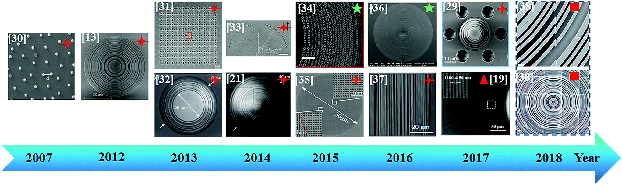 | ||
| Fig. 1 Development of fabrication technologies for SOLs. Note: The cross in red means devices fabricated by FIB milling, the pentacle in green stands for the devices fabricated via EBL, the triangle in red means the devices are fabricated by DLW and the square in red indicates the devices fabricated by DUV. | ||
Such centimeter-scale, light weight and low-cost lenses accompanied by flexible customized optical patterns can develop their wide applications in interdisciplinary fields including parallel particle trapping, full-color high-resolution imaging, and compact spectral imaging systems.
Materials and methods
Flexible focusing pattern realization of sub-diffraction planar SOLs
When planar SOLs are normally illuminated by the broadband incident plane wave, the normal optical distribution after the lens surface is shown in Fig. 2.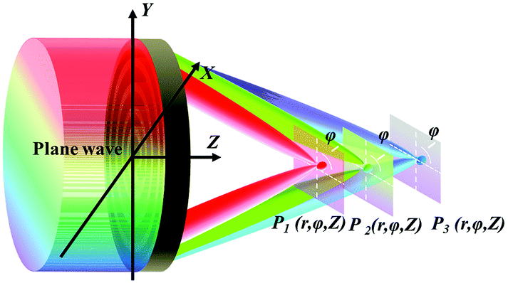 | ||
| Fig. 2 Schematic illustration of sub-diffraction-limit focusing by SOLs, behaving like common diffractive optical elements (DOEs). | ||
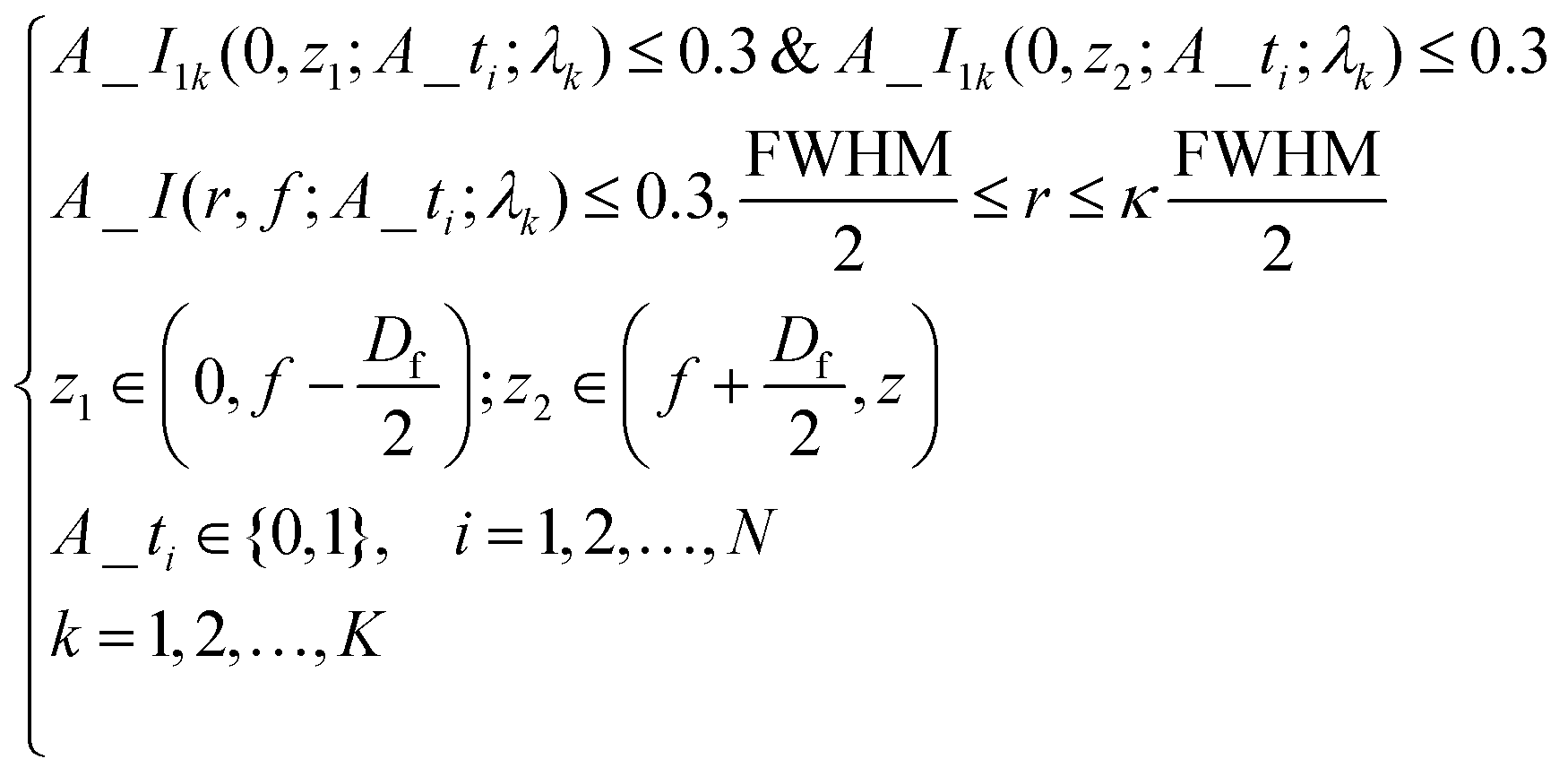
To provide a general programming model for controllably designing SOLs, we restrain the intensity I along two orthogonal directions, including the optical axis and transverse axes in every focal plane. A specific fluctuation range of the side lobe is set to ensure the light field as required. If the value is improper, it may be difficult to converge to an optimal solution. After evaluating the energy distribution between the side lobe and the central spot, a side lobe factor of 0.3 is chosen in our design. We employ the GA based on the MATLAB programming language to design binary phase-type (0, π) SOLs that implement the predefined axial-intensity modulation over a given region. Hence, a general universal optimization model is built up as in eqn (1) and (2).
Minimize
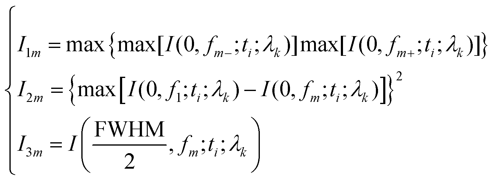 | (1) |
Subject to
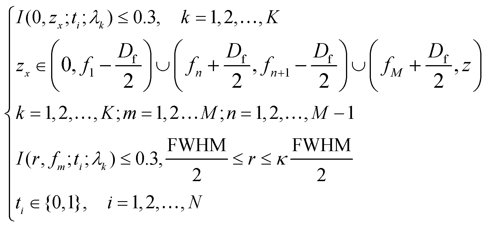 | (2) |
Here, we assign a weighted coefficient wj to each objective function Ij, so that the problem can be converted to a single-objective problem with the objective function defined as in eqn (3).
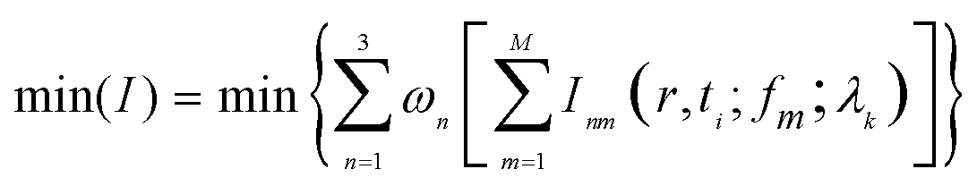 | (3) |
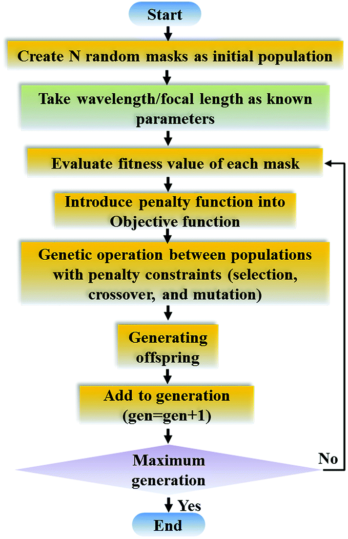
In our previous iterative processes,23,24 the constrained conditions were directly put into the algorithm to select the optimal solution with a distinct divergence. Indeed, there is always a need for a large number of initial individuals to launch the optimization and the desired results could not be generated at once. To solve the mentioned issue, the constrained conditions are changed as penalty function and put into the iterative process in which the parameters can be tuned according to the specific demands on the SOLs. Obviously, the multi-objective and multi-constraint optimization problem can now be transformed to the unconstrained multi-objective problem, resulting in a highly efficient optimization process. Therefore, the whole algorithm is made more flexible and can be utilized to controllably design SOLs according to specific applications. The entire design procedure is illustrated in Fig. 3. The major steps are as follows: first, to create random masks as initial populations and calculate objective functions for different focal lengths and wavelengths of each mask served as the fitness value; second, to change the given constrains as penalty functions and add to the objective functions; third, to iteratively perform the genetic operations among the population (selection, crossover and mutation) and reinsert the offspring population to the original parental population according to the fitness value of each mask until the termination criterion is satisfied. In the end, the best structural mask in the population is achieved. To realize arbitrarily focusing optical patterns designed for the planar SOLs, the super-resolution multifocal SOL and achromatic SOL are optimized which can find their wide uses in parallel particle trapping and high-resolution label-free microscopy instead of the traditional bulky and complicated DOEs. Furthermore, the achromatic-customized SOL based on the proposed flexible algorithm is firstly demonstrated to expand its new applications in the compact diffractive spectral imaging system. What should be also mentioned here is that the diameters of the designed SOLs are all set as large as 12 mm to enhance their compatibility with the commercialized optical system. Moreover, the 30 μm smallest annular size of the designed SOLs makes it possible to fabricate the centimeter-scale device through the normal lithography process. To verify the calculation efficiency of the proposed algorithm, the GA performance tracking of the designed three SOLs is illustrated in the ESI.† It is noteworthy that the three SOLs can be obtained just through nearly 20 generations regardless of their large dimensions, and a highly efficient and convergent iterative process can be developed.
 | ||
| Fig. 3 The optimization procedure for arbitrarily focusing pattern design of planar SOLs. | ||
For clarity, three SOLs with various purposes, i.e. for the multifocal optical field, for the achromatic case and achromatic-customized design, are denoted as sample #1, #2, and #3 in the following discussion, respectively. The detailed design parameters and the corresponding calculated Rayleigh diffraction limit for SOLs #1–#3 are given in the ESI.†
Parallel fabrication of planar SOLs
The existing fabrication technologies of SOLs are mainly concentrated in the FIB milling or EBL method. Benefiting from the 30 μm smallest groove width, we establish a parallel-fabrication flow for centimeter-scale planar dielectric SOLs, as shown in Fig. 4. First, a SixNy layer is deposited on a 4-inch pyrex glass substrate by plasma-enhanced chemical vapor deposition (PECVD), followed by the normal lithography process. Then, reactive ion etching (RIE) is progressed to form the desired non-subwavelength SixNy ring belts. The lift-off process to evaporate the chromium (Cr) layer is for defining opening windows to block the unwanted surrounding light passing through SOLs. As shown in the ESI,† the measured refractive index of the SixNy layer was about 2.25 at the wavelength of 532 nm, and the SixNy ring belts were fabricated with 231 nm thickness to achieve a phase difference of π. Fig. 5 presents a sketching diagram of wafer-level planar SOLs and the scanning electron microscopy (SEM) image giving the zoom-in view. To illustrate the macroscopic size of the centimeter-scale SOLs with specific focusing patterns, as shown in Fig. 5, a typical achromatic-customized SOL is demonstrated together with a coin and the corresponding micrometer-scale feature size can also be observed. Notably, the fabrication error generated by the basic lithography can be controlled within ±0.5 μm, resulting in the focusing performance of SOLs without significant deviation from the design.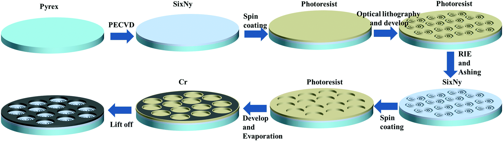 | ||
| Fig. 4 The 4-inch wafer-level fabrication flow of SOLs. | ||
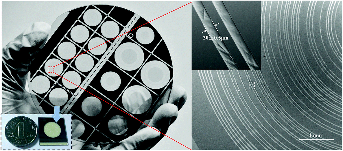 | ||
| Fig. 5 The device images obtained by both optical and electronic microscopes for the fabricated SOLs. | ||
Results and discussion
Multifocal SOL
A sub-diffraction multifocal focusing lens would be valuable in many applications, most notably parallel particle trapping and three-dimensional imaging systems.40,41 We consider the design of a SOL that produces three focal spots with equal intensity distribution and spacing along the Z axis at 532 nm. Here, the optimization model to control the multifocal field's prescribed parameters is built up as in eqn (4) and (5). The three focal spots are discretely located at 5990, 6000 and 6010 μm away from the output surface of the SOL. For experimental characterization, the transmitted light patterns are collected using a 100×/0.9 Nikon inverted microscope objective and a suitable high-resolution camera slice by slice with an axial step of 100 nm (see the ESI†). The computed axial intensity distribution of the multifocal SOL is depicted in Fig. 6a. Meanwhile, the practically measured axial light intensity distributions are demonstrated in Fig. 6b. As shown in Fig. 6c, compared with the simulation, the experimental result shows a slight deviation, which can be attributed to the fabrication imperfections. The simulated and experimental light intensity distributions along the focal planes at the locations of 5990, 6000, and 6010 μm (marked by A–A, B–B, C–C and A′–A′, B′–B′, C′–C′, respectively) are also given (see Fig. 6d and e). The simulated FWHMs for the three discrete focal points are 0.83λ, 0.70λ, and 0.83λ, respectively. In contrast, the experimentally measured FWHMs are (0.83 ± 0.15)λ, (0.68 ± 0.05)λ, and (0.84 ± 0.15)λ, respectively. The results are the average of three measurements. As expected, the simulated and experimental hotspot sizes are all beyond the calculated Rayleigh diffraction limit 0.86λ, and a good agreement is achieved. According to the flexible control over the light field with the optimization model, more focal spots such as four foci with controllable axial distribution can be similarly designed along the optical axis, as reported in our recent work.24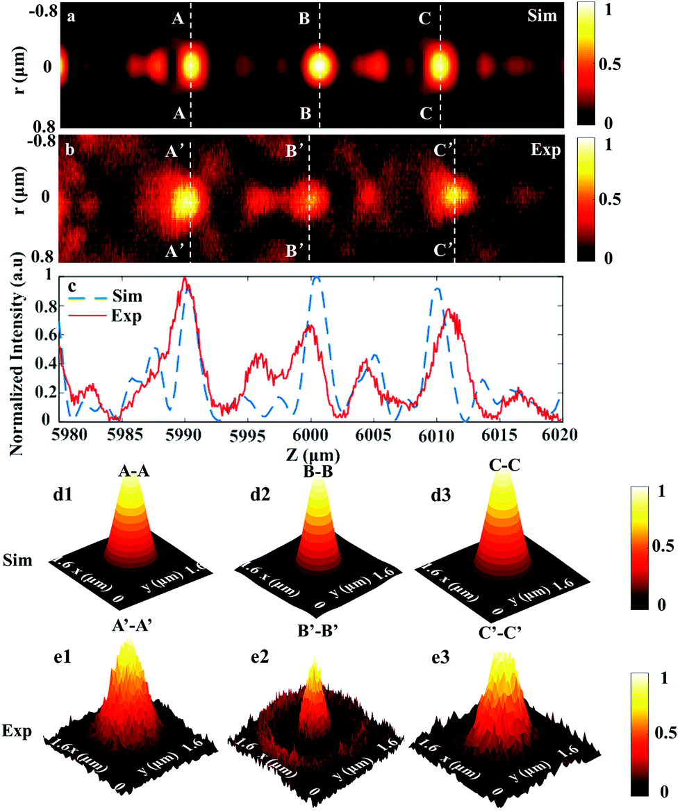 | ||
| Fig. 6 Simulated and experimental results of the multifocal SOL at 532 nm. (a) Simulated and (b) experimental light distributions in the X–Z cross-section; (c) the corresponding axial intensity distribution along the optical axis for both simulation and experiment; (d) theoretical distributions in the three focal planes located at the longitudinal positions of 5990, 6000, and 6010 μm (marked by regions A–A, B–B, and C–C); (e) experimental results in the discrete three focal planes located at longitudinal positions of 5990, 6000, and 6010 μm (marked by regions A′–A′, B′–B′, and C′–C′). | ||
The designed centimeter-scale ultrathin multifocal SOL can make its great progress in the miniaturization of optical systems such as imaging systems, detectors, optical data storage, laser printing, optical free-space communications etc.
Minimize
 | (4) |
Subject to
 | (5) |
Achromatic SOL
High-resolution full-color imaging applications raise a strict requirement for the existing optical lenses. The hybrid refractive-diffractive doublets have been put forward to solve the dispersive problem of traditional lenses,42 while the bulky form and poor imaging quality can still be the major challenges. On the other hand, metalenses with subwavelength feature sizes have been recently exploited to fulfill the broadband achromaticity through constructing a certain wavefront profile.43–45 Although successful, these strategies add fabrication complexity and high cost to optical systems. Owing to the flexible design and ability of parallel fabrication, achromatic SOLs can be a priority for future high-resolution broadband imaging applications. However, the previous report just made the focal points of different wavelengths overlap to achieve a nominal achromatic SOL.27 In this work, a much more universal optimization model to construct the achromatic optical pattern is established as in eqn (6) and (7). Based on the iterative process, a SOL that can directly focus at three discrete wavelengths can be achieved. For the long working distance and large size, especially the high-resolution case, a centimeter-scale achromatic SOL can be a good choice for compact and light weight broadband imaging systems.Minimize
 | (6) |
Subject to
 | (7) |
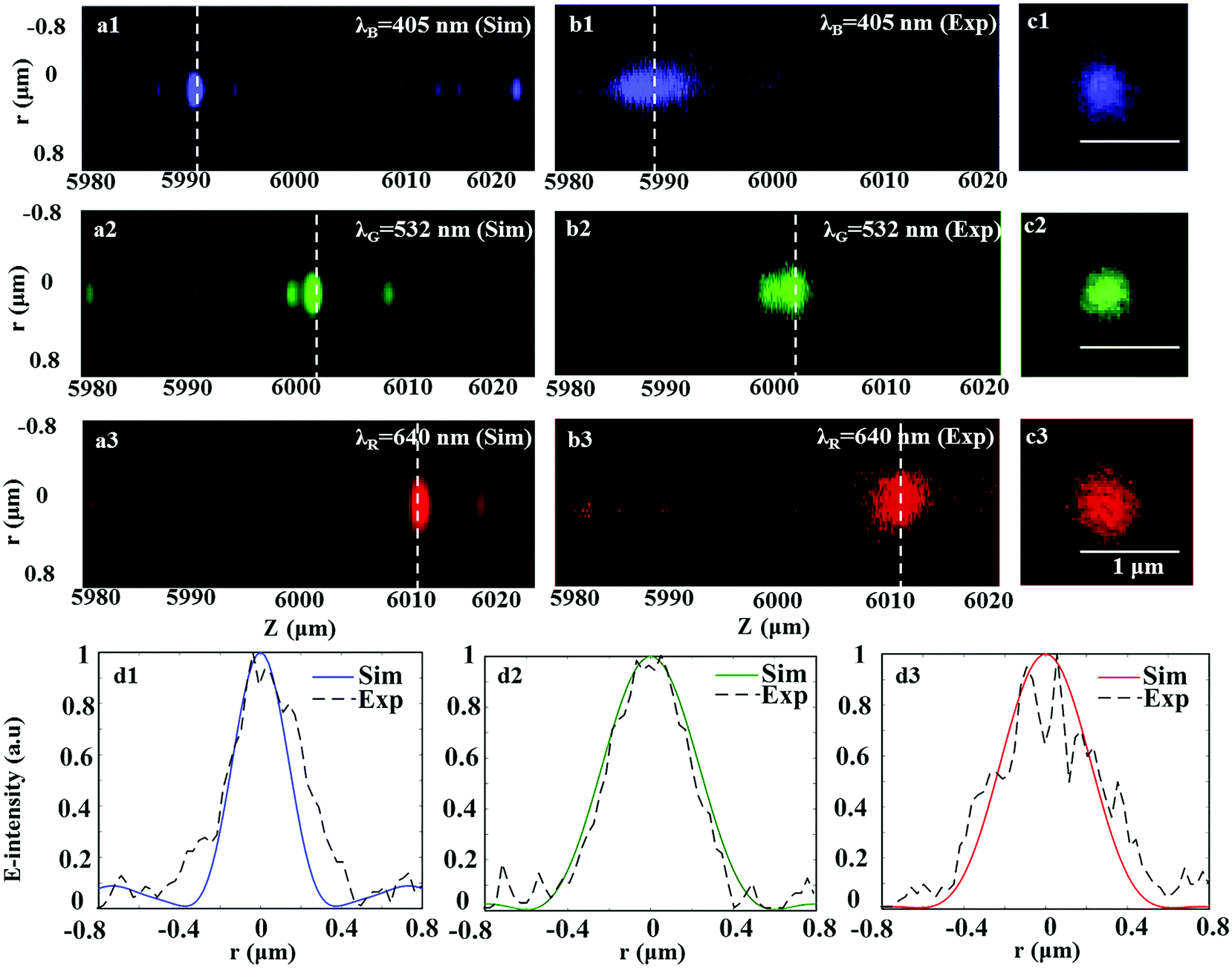
To illustrate the proposed optimization model, we design a SOL that could simultaneously focus the three primary colors at the same position, producing intuitively perceived white light. As is well known, these three colors can be mixed to generate a computer display. The computed intensity distributions in the longitudinal cross-section are presented in Fig. 7a. The corresponding experimental data are shown in Fig. 7b. The optical contours in the focal planes for R, G and B wavelengths are screened in Fig. 7e1–e3. The corresponding normalized intensity distributions are also shown in Fig. 7d, which shows an excellent agreement with each other. The detailed computed hotspot sizes reach 0.74λR at λR = 640 nm, 0.81λG at λG = 532 nm and 0.74λB at λB = 405 nm. Besides, the experimental hotspots for the three wavelengths were (0.74 ± 0.02)λR, (0.81 ± 0.01)λG and (0.74 ± 0.02)λB, respectively. Obviously, the computed and measured results are all beyond the Rayleigh diffraction limit. As expected, we could acquire a ‘white’ sub-diffraction hotspot by fusing the images of the three selected RGB wavelengths as seen in Fig. 7e4.
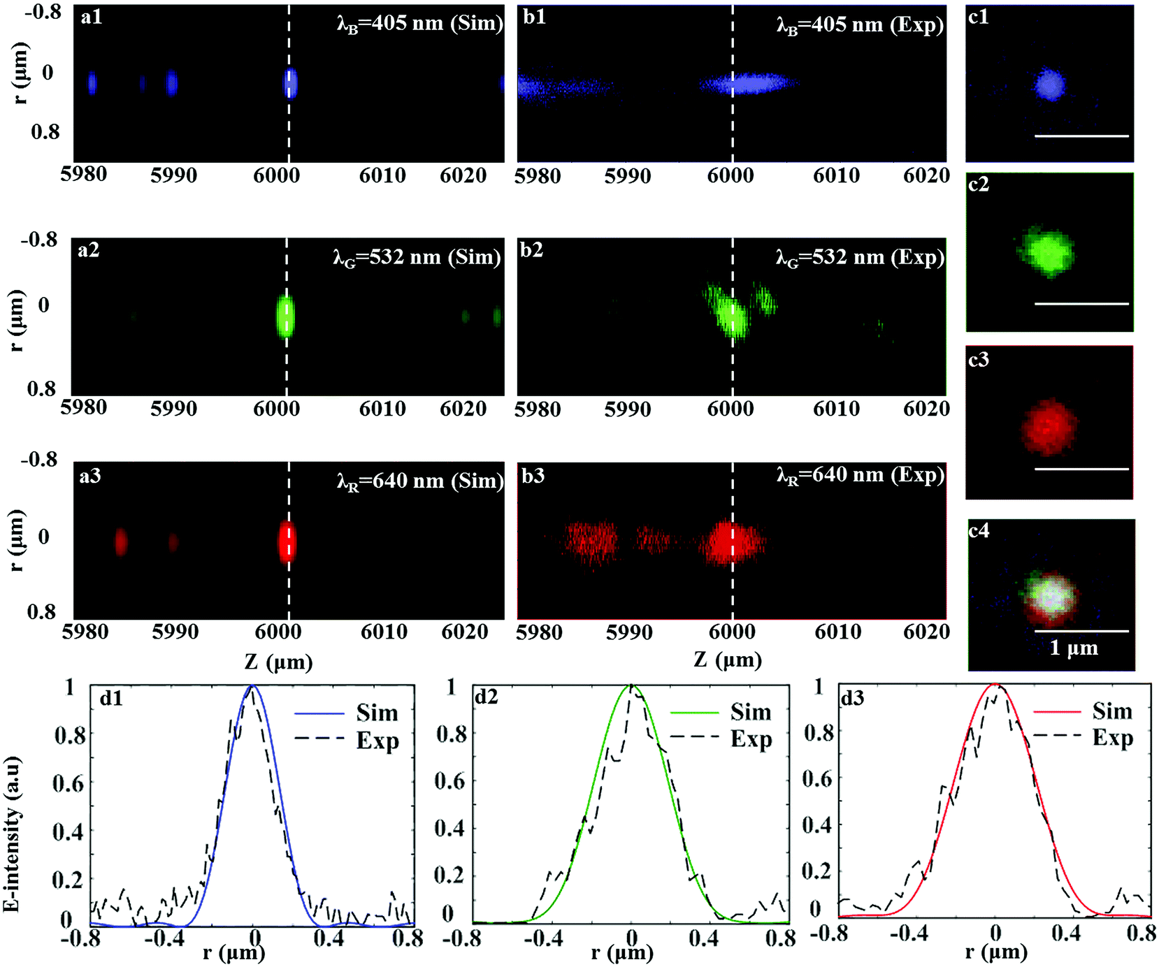 | ||
| Fig. 7 Planar achromatic SOL. (a) Simulated and (b) experimental focusing patterns in the X–Z cross-section. The vertical dashed white lines indicate the focal planes. (c) Experimentally registered intensity patterns in the transverse focal plane: (c1) for λB, (c2) for λG, (c3) for λR and (c4) for the fused image by RGB wavelengths. (d) The simulated and experimental normalized intensity distributions in the transverse focal plane along the dashed lines through the focal points: (d1) for λB, (d2) for λG, and (d3) for λR. Images are all captured by a color built-in CCD camera in the microscope. | ||
Actually, we didn't consider the material dispersion induced phase modulation difference at other wavelengths (>π for short wavelengths, <π for longer wavelengths) in the optimization process. To verify the robustness of the focusing behaviour on the non-ideal 0/π phase modulation, the optimized phase transmittance has been changed to 0/0.873π and 0/1.5π, and the focusing patterns of the achromatic SOL are shown in the ESI.† We can find out that the two kinds of non-ideal phase modulation seem to function little on the focusing behavior of the achromatic SOL, which shows a relatively good robustness in the dielectric layer. Nonetheless, the suitable phase modulation matching with the corresponding incident wavelength should be taken into consideration in the optimization to obtain a more precise control over the focal contours of the achromatic SOL. Additionally, more than three wavelengths can be designed in the same way based on the proposed algorithm (see the ESI†), and a continuously broadband achromatic SOL can be achieved in the near future.
Achromatic-customized SOL
The normal dispersive rule of planar SOLs for red (λR = 640 nm), green (λG = 532 nm) and blue (λB = 405 nm) light is illustrated in Fig. 2. Different from the refractive lens, the dispersive feature of the diffractive lens produces a shorter focal length for a longer wavelength. A planar SOL is a kind of DOE whose dispersive property had been experimentally characterized in our latest publication.46 Based on the proposed universal algorithm, a reverse design of dispersive property is considered. The detailed optimization model for the purpose can be realized as in eqn (8) and (9). The targeted working distances of the achromatic-customized SOL for red (λR = 640 nm), green (λG = 532 nm) and blue (λB = 405 nm) lights are 6010, 6000, and 5990 μm, respectively. Indeed, the presented design seems to be totally customized. Since the DOEs have played a critical role in the spectral imaging system which can drastically decrease the volume of the conventional bulky system, they could be the main trend for the future integration of optical systems. Additionally, the achromatic-customized SOL can also be treated as a beam-splitting element in the spectrometer to replace the traditional counterpart, which has to rely on long light propagation paths to achieve sufficient dispersion, making the whole system bulky and inconvenient for integration. Note that this is the first novel demonstration of a planar SOL which may open up a new research point for this kind of optical element.Minimize
 | (8) |
Subject to
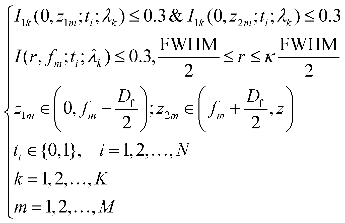 | (9) |
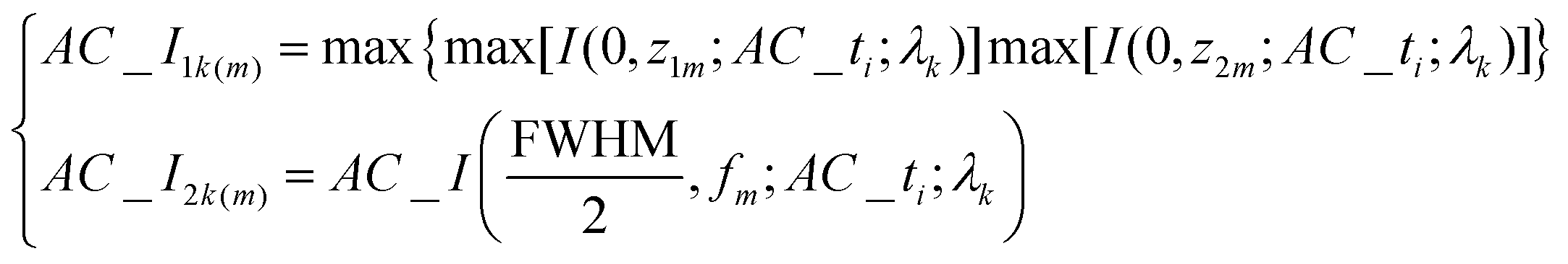
The computed intensity distributions in the longitudinal cross-section are presented in Fig. 8a. The corresponding experimental data are shown in Fig. 8b. The optical contours in the focal planes for R, G and B wavelengths are screened in Fig. 8e1–e3. The corresponding normalized intensity distributions for the simulated and experimental ones in the focal planes are also shown in Fig. 8d, which shows a good agreement with each other. The detailed computed hotspot sizes are 0.77λR at λR = 640 nm, 0.78λG at λG = 532 nm and 0.77λB at λB = 405 nm, respectively. Correspondingly, the experimental hotspots for the three wavelengths are (0.77 ± 0.02)λR, (0.78 ± 0.06)λG and (0.80 ± 0.05)λB, respectively. The computed and measured results are all beyond the Rayleigh diffraction limit except for the one at λB, whose causes are still under investigation, mainly from two aspects, i.e. fabrication imperfections and measurement errors. For the blue wavelength, the detector built in the customized system seems to show a sensitive response to the wavelength and the homemade fiberized coupled laser of 405 nm seems to show a relatively worse stability which may lead to the increasing depth of focus at the wavelength of 405 nm. Additionally, the slight divergence of the incoming light (the fiber collimator only works well for the limited spectral range) may also influence the focusing performance of SOLs. In line with the designs of multifocal and achromatic SOLs, the number of wavelengths concerned is not a limitation on employing the proposed optimization method.
 | ||
| Fig. 8 Planar achromatic-customized SOL. (a) Simulated and (b) experimental diffraction patterns in the X–Z cross-section. The vertical dashed white lines indicate the focal planes. (c) Experimentally characterized intensity distributions in the transverse focal planes: (c1) for λB, (c2) for λG, and (c3) for λR. (d) The simulated and experimental normalized intensity distributions in the transverse focal plane along the dashed lines through the focal points: (d1) for λB, (d2) for λG, and (d3) for λR. Images are all captured by a color built-in CCD camera in the microscope. | ||
The findings can pave the way for a new model to establish spectral imaging systems and data storage. Besides, the high freedom of controlling the optical components according to the customized requirements can increase the performance and number of functionalities of this kind of light weight planar optical device.
Conclusions and outlook
We have proposed an unconstrained multi-objective optimization of wafer-level planar SOLs in which the initial constraint conditions were changed to a penalty function, making the optimization process converge easily. Compared with the previous algorithm in our recent publications, the newly proposed algorithm is flexible and can be applied for designing arbitrary focusing patterns of centimeter-scale planar SOLs efficiently and quickly. 12 mm diameter planar SOLs with a feature size of 30 μm were designed to achieve multifocal, achromatic, and achromatic-customized focusing fields.To conduct the low-cost and parallel fabrication of planar optical elements, we put forward a wafer-level fabrication of planar SOLs in which the normal lithography process has been utilized instead of the high cost fabrication ways such as FIB milling and EBL methods. We experimentally demonstrate the far-field focusing properties of the three designed SOLs. Encouragingly, the obtained results agree well with the simulations. The developed SOLs create sub-diffraction hotspots by delicate constructive interference of propagating optical waves and can be tuned intricately to achieve a desired light field. Since less ring belts can lead to a coarse regulation of the light field after the lens surface, an increased number of concentric rings can contribute to the interference of diffracted beams and enlarge the degrees of freedom in optimization design, especially for broadband cases. It's worth noting that most of the light energy of SOLs is contributed to the large side lobes around the central sub-diffraction-limit hotspots, and there needs a tradeoff between the spot size and focusing efficiency. Similar to the binary phase-type Fresnel zone plate (FZP), being famous as diffractive lenses, the maximum efficiency that can be achieved is always limited to around 40% in theory.17,47 As a matter of fact, the low level of throughput efficiency may be prohibitive for some demanding applications but may be tolerable for others. For phase-type SOLs, multiple phase levels instead of the binary phase would be beneficial to reduce the side lobes and increase the focusing efficiency. Besides, the low focusing efficiency of SOL could be still applicable for practical applications in the case of high-energy laser sources and high-sensitivity detectors. Additionally, the proposed design methods can be available for all the wavelengths.
The unprecedented design freedom of planar SOLs will greatly expand the range of applications of micro-optics and integrated optics. We hope that the designed and fabricated centimeter-scale multifocal SOL, achromatic SOL and achromatic-customized SOL can serve as powerful super-resolution focusing and imaging tools for a wide range of applications in parallel data storage, high-resolution broadband noninvasive imaging, low-cost fiberized microscopy, portable Raman spectrometers for super-resolution bio-imaging, optical coherence tomography imaging and micro/nanofabrication.
Conflicts of interest
There are no conflicts to declare.Acknowledgements
We acknowledge the financial support by the National Natural Science Foundation of China (51622509), the Fundamental Research Funds for the Central Universities (3102017jg02007), the Strategic Initiative Project, the 111 Project (B13044), and the Excellent Doctorate Cultivating Foundation of Northwestern Polytechnical University. We would also like to thank the Analytical & Testing Center of Northwestern Polytechnical University for the fabrication of SOL samples.References
- E. Beizig, J. K. Trautman, T. D. Harris, J. S. Weiner and R. L. Kostelak, Science, 1991, 251, 1468–1470 CrossRef PubMed.
- Z. Liu, H. Lee, Y. Xiong, C. Sun and X. Zhang, Science, 2007, 315, 1686 CrossRef CAS.
- X. J. Ni, S. Ishii, A. V. Kildishev and V. M. Shalaev, Light: Sci. Appl., 2013, 2, e72 CrossRef.
- A. I. Fernandez-Dominguez, Z. Liu and J. B. Pendry, ACS Photonics, 2015, 2, 341–348 CrossRef CAS.
- X. H. Dong, A. M. H. Wong, G. V. Eleftheriades, M. Kim and V. E. George, Optica, 2017, 4, 1126 CrossRef.
- D. Matsunaga, S. Sato and Y. Kozawa, Optica, 2018, 5, 86 CrossRef.
- J. Chen, M. Badioli, P. A. Gonzalez, S. Thongrattabasiri, F. Huth, J. Osmond, M. Spasenovic, A. Centeno, A. Pesquera, P. Godignon, A. Z. Elora, N. Camara, F. Javier Garcia de Abajo, R. Hillenbrand and F. H. L. Koppens, Nature, 2012, 487, 77–81 CrossRef CAS.
- G. Y. Lee, G. Yoon, S. Y. Lee, H. Yun, J. Cho, K. Lee, H. Kim, J. Rho and B. Lee, Nanoscale, 2018, 10, 4237–4245 RSC.
- M. Papaioannou, E. Plum, J. Valente, E. T. F. Rogers and N. I. Zheludev, Light: Sci. Appl., 2016, 5, e16070 CrossRef CAS.
- F. Aieta, M. A. Kats, P. Genevet and F. Capasso, Science, 2015, 347, 1342–1345 CrossRef CAS.
- W. Liu, Z. Li, H. Cheng, C. Tang, J. Li, S. Zhang, S. Chen and J. Tian, Adv. Mater., 2018, 30, 1706368 CrossRef.
- E. Arbabi, A. Arbabi, S. M. Kamali, Y. Horie, M. Faraji-Dana and A. Faraon, Nat. Commun., 2018, 9, 812 CrossRef.
- E. T. F. Rogers, J. Lindberg, T. Roy, S. Savo, J. E. Chad, M. R. Dennis and N. I. Zheludev, Nat. Mater., 2012, 11, 432–435 CrossRef CAS.
- R. Remez, Y. Tsur, P. H. Lu, A. H. Tavabi, R. E. Dunin-Borkowski and A. Arie, Phys. Rev. A: At., Mol., Opt. Phys., 2017, 95, 031802(R) CrossRef.
- K. Huang, H. Ye, J. Teng, S. P. Yeo, Luk’ Boris and C. W. Qiu, Laser Photonics Rev., 2014, 8, 152–157 CrossRef CAS.
- Y. Eliezer and A. Bahaba, Optica, 2017, 4, 440–446 CrossRef.
- K. Huang, F. Qin, H. Liu, H. Ye, C. Qiu, M. Hong, B. Luk'Yanchuk and J. Teng, Adv. Mater., 2018, 1704556 CrossRef PubMed.
- Y. Eliezer and A. Bahabad, ACS Photonics, 2016, 3, 1053–1059 CrossRef CAS.
- F. Qin, K. Huang, J. Wu, J. Teng, C. W. Qiu and M. Hong, Adv. Mater., 2017, 29, 1602721 CrossRef PubMed.
- C. Hao, Z. Nie, H. Ye, H. Li, Y. Luo, R. Feng, X. Yu, F. Wen, Y. Zhang, C. Yu, J. Teng, B. Luk'yanchuk and C. Qiu, Sci. Adv., 2017, 3, e1701398 CrossRef.
- K. S. Rogers, K. N. Bourdakos, G. H. Yuan, S. Mahajan and E. T. F. Rogers, Opt. Express, 2018, 26, 8095–8112 CrossRef PubMed.
- G. Yuan, E. T. F. Rogers, T. Roy, G. Adamo, Z. Shen and N. I. Zheludev, Sci. Rep., 2014, 4, 6333 CrossRef CAS.
- J. S. Diao, W. Z. Yuan, Y. T. Yu, Y. C. Zhu and Y. Wu, Opt. Express, 2016, 24, 1924–1933 CrossRef PubMed.
- M. Y. Li, W. L. Li, H. Y. Li, Y. C. Zhu and Y. T. Yu, Sci. Rep., 2017, 7, 01335 CrossRef.
- S. Yan, B. Yao, W. Zhao and M. Lei, J. Opt. Soc. Am. A, 2010, 27, 2033–2037 CrossRef.
- Y. Yu and Q. Zhan, Sci. Rep., 2015, 5, 14673 CrossRef CAS.
- J. Hu, C. H. Liu, X. Ren, L. J. Lauhon and T. W. Odom, ACS Nano, 2016, 10, 10275–10282 CrossRef CAS PubMed.
- O. Avayu, E. Almeida, Y. Prior and T. Ellenbogen, Nat. Commun., 2017, 8, 14992 CrossRef CAS PubMed.
- G. H. Yuan, E. T. F. Rogers and N. I. Zheludev, Light: Sci. Appl., 2017, 6, e17036 CrossRef CAS PubMed.
- F. M. Huang, Y. Chen, F. J. G. de Abajo and N. I. Zheludev, J. Opt. A: Pure Appl. Opt., 2007, 9, S285–S288 CrossRef.
- T. Roy, E. T. Rogers and N. I. Zheludev, Opt. Express, 2013, 21, 7577–7582 CrossRef PubMed.
- E. T. F. Rogers, S. Savo, J. Lindberg, T. Roy, M. R. Dennis and N. I. Zheludev, Appl. Phys. Lett., 2013, 102, 181109 CrossRef.
- G. Yuan, E. T. F. Rogers, T. Roy, L. Du, Z. Shen and N. I. Zheludev, Lasers and Electro-Optics, in IEEE, 2014, pp. 1–2 Search PubMed.
- K. Huang, H. Liu, F. J. Garcia-Vidal, M. Hong, B. Luk'yanchuk, J. Teng and C. W. Qiu, Nat. Commun., 2015, 6, 7059 CrossRef CAS PubMed.
- D. Tang, C. Wang, Z. Zhao, Y. Wang, M. Pu, X. Li, P. Gao and X. Luo, Laser Photonics Rev., 2015, 9, 713–719 CrossRef CAS.
- A. Yu, G. Chen, Z. Zhang, Z. Wen, L. Dai, K. Zhang, S. Jiang, Z. Wu, Y. Li, C. Wang and X. Luo, Sci. Rep., 2016, 6, 38859 CrossRef CAS.
- G. H. Yuan, S. Vezzoli, C. Altuzarra, E. T. F. Rogers, C. Couteau, C. Soci and N. I. Zheludev, Light: Sci. Appl., 2016, 5, 16127 CrossRef PubMed.
- H. Ni, G. Yuan, L. Sun, N. Chang, D. Zhang, R. Chen, L. Jiang, H. Chen, Z. Gu and X. Zhao, RSC Adv., 2018, 8, 20117–20123 RSC.
- A. E. Siegman, Quasi fast Hankel transform, Opt. Lett., 1977, 1, 13–15 CrossRef CAS.
- X. Chen, M. Chen, M. Q. Mehmood, D. Wen, F. Yue, C. W. Qiu and S. Zhang, Adv. Opt. Mater., 2015, 3, 1201–1206 CrossRef CAS.
- Z. Zhang, D. Wen, C. Zhang, M. Chen, W. Wang, S. Chen and X. Chen, ACS Photonics, 2018, 5, 1794–1799 CrossRef CAS.
- A. Flores, M. R. Wang and J. J. Yang, Appl. Opt., 2004, 43, 5618 CrossRef.
- S. Wang, P. C. Wu, V. C. Su, Y. C. Lai, M. K. Chen, H. Y. Kuo, B. H. Chen, Y. H. Chen, T. T. Huang, J. H. Wang, R. M. Lin, C. H. Kuan, T. Li, Z. Wang, S. Zhu and D. P. Tsai, Nat. Nanotechnol., 2018, 13, 227 CrossRef CAS PubMed.
- W. T. Chen, A. Y. Zhu, V. Sanjeev, M. Khorasaninejad, Z. Shi, E. Lee and F. Capasso, Nat. Nanotechnol., 2018, 13, 220 CrossRef CAS.
- Z. Li, T. Zhang, Y. Wang, W. Kong, J. Zhang, Y. Zhang, C. Wang, X. Li, M. Pu and X. Luo, Laser Photonics Rev., 2018, 1800064 CrossRef.
- Y. Yu, W. Li, H. Li, M. Li and W. Yuan, Nanomaterials, 2018, 8, 185 CrossRef.
- M. Beresna, M. Gecevicius and P. G. Kazansky, Opt. Mater. Express, 2011, 1, 783–795 CrossRef.
Footnote |
| † Electronic supplementary information (ESI) available: details of performance tracking, design parameters, optical measurement, and super-achromatic SOL design. See DOI: 10.1039/c8nr07985d |
| This journal is © The Royal Society of Chemistry 2019 |