DOI:
10.1039/C8NR07692H
(Paper)
Nanoscale, 2019,
11, 356-364
Cr2TiC2-based double MXenes: novel 2D bipolar antiferromagnetic semiconductor with gate-controllable spin orientation toward antiferromagnetic spintronics†
Received
21st September 2018
, Accepted 27th November 2018
First published on 27th November 2018
Abstract
Antiferromagnetic (AF) spin devices could be one of the representative components for applications of spintronics thanks to the numerous advantages such as resistance to magnetic field perturbation, stray field-free operation, and ultrahigh device operation speed. However, detecting and manipulating the spin of AF materials is still a major challenge due to the absence of a net magnetic moment and spin degeneracy in the band structure. Bipolar antiferromagnetic semiconductors are promising solutions to these problems. Herein, using density functional theory calculations, we present asymmetrical functionalized double MXenes (Cr2TiC2FCl) that behave as a novel bipolar antiferromagnetic semiconductor (BAFS) with vanishing magnetism, in which the valence band and conduction band around the Fermi level exhibit opposite spin directions. Remarkably, gate voltage can manipulate the spin orientation of the AF Cr2TiC2FCl and lead to a transition from BAFS to half-metal antiferromagnets (HMAF). Moreover, the mixed functionalized double MXenes with various F/Cl concentrations show the BAFS feature due to the different chemical environment for the Cr atom. Our results presented herein open a new strategy towards AF spintronics and the realization of the AF spin field effect transistor.
1. Introduction
Spintronics, which employs the spin degree of freedom of electrons for information storage, transportation and processing, is one of the most promising technologies for next-generation information engineering.1 The development of spintronic devices relies on finding new materials with specific magnetic properties. Generally, the magnetic order in materials can be manipulated by the magnetic field approach,2 while materials with considerable spin-orbital coupling can be controlled by the electric field.3 2D materials have attracted extensive research interest due to their many intriguing physical and chemical properties. In particular, 2D magnetic materials are predicted to have high spin-polarization and room-temperature magnetic order, which are of great advantage for spintronic applications. Recently, some 2D magnetic materials with intrinsic ferromagnetism and high spin-polarization have been extensively studied, such as transition-metal (TM) halides,4–7 MXenes,8–10 CrATe3 (A = Si, Ge and Sn),11,12 TM dihydride13 and Janus TMDs,14 which show promising applications in spintronic devices. Particularly, 2D ferromagnetism has been discovered experimentally in atom-thick CrI3 and CrGeTe3 crystals.15,16 Subsequently, room-temperature ferromagnetism characteristics were found in 2D VSe2/MoS2 van der Waals heterostructures and epitaxial MnSe2 films.17,18 These experimental achievements of intrinsic 2D magnetic materials have attracted huge interest for the exploration of new physical properties and phenomena. For instance, numerous studies have been devoted to electrically and magnetically manipulate spin-related properties, e.g., Dzyaloshinskii–Moriya interaction, interlayer spin–flip and magnetic anisotropy.19–24 Furthermore, 2D magnetic materials exhibit intriguing physical properties, such as multiferroics,25,26 thermoelectrics,27 quantum anomalous Hall effect7 and valleytronics.28
However, so far, most of the theoretical and experimental studies focused on ferromagnetic (FM) order. The existence of stray magnetic fields in FM materials will unavoidably limit the generation and complete manipulation of spin-polarized carriers.29 In principle, antiferromagnetic (AF) materials possess intrinsic advantages, including robustness against magnetic field perturbation, no stray fields, and ultrahigh speed of device operation, which have attracted significant attention due to their great potential in AF spintronics.30 Until now, however, manipulating and detecting the spin structure in AF materials has been proved challenging due to the absence of a net magnetic moment and spin degeneracy in the band structure.
To overcome these bottlenecks, Van Leuken and de Groot31 proposed the concept of half-metallic antiferromagnets (HMAF) using CrMnSb Heusler compounds as examples. Such HMAF materials combined with high spin-polarization and AF order, offer new opportunities to manipulate and detect the spin in AF materials. Particularly, the HMAF properties in the Half-Heusler Mn2RuxGa and Mn2PtxGa alloys have been confirmed experimentally.32,33 However, to date, only a few 2D AF systems have been predicted to have high spin-polarization, e.g., TM co-doped 2D semiconductor.10,34,35 The transition metal carbides/nitrides, known as MXenes, are a family of 2D materials, which have been synthesized experimentally by the chemical exfoliation technique.36,37 However, the magnetism and spin-polarization of MXenes generally disappear when their surfaces are functionalized, as reported in Cr2CT2, V2CT2 and Cr2TiC2T2 (T = F, OH) MXenes.8,38,39
In this paper, using first-principles calculations, we propose that a bipolar antiferromagnetic semiconductor with vanishing magnetism can be achieved in double MXenes Cr2TiC2 by using F and Cl atoms asymmetrically with mixed functionalization. The application of gate voltage can easily manipulate the spin direction, leading to the transition from BAFS to half-metal antiferromagnets. The underlying mechanisms are explained based on the band structure analysis.
2. Computational method and details
We performed first-principles calculations within the density functional theory (DFT) using the projector augmented wave method as implemented in the plane-wave code VASP (version 5.4.1) with the Perdew–Burke–Ernzerhof (PBE) exchange–correlation functional.40–42 The criteria of energy and atom force convergence were set to be 10−5 eV per unit cell and 0.01 eV Å−1, respectively. The Brillouin zone (BZ) was sampled using 15 × 15 × 1 and 21 × 21 × 1 Gamma-centered Monkhorst–Pack grids for the structural relaxation and electronic structure calculations, respectively. For the magnetic properties calculation, the Hubbard “U” correction was employed within the rotationally invariant DFT+U approach proposed by Dudarev et al.43 A correction of U = 3 eV was employed based on the relevant previous reports.10 The band structure calculations for symmetrical and asymmetrical functionalization of Cr2TiC2 were performed using the screened-nonlocal exchange Heyd–Scuseria–Ernzerhof (HSE06) functional of the generalized Kohn–Sham scheme. The phonon frequencies were calculated using a supercell approach as implemented in the PHONOPY code.44,45
3. Results and discussion
3.1 Symmetrical functionalization of Cr2TiC2
Before presenting the results for asymmetrically functionalized Cr2TiC2, we firstly discuss the structure, electronic and magnetic properties of symmetrically functionalized MXenes, including Cr2TiC2F2 and Cr2TiC2Cl2 sheets. The calculated lattice constants for Cr2TiC2F2 and Cr2TiC2Cl2 sheets are 3.03 Å and 3.14 Å, respectively, which are in good agreement with previous calculations.39 The band structure (see Fig. S1†) shows that both the Cr2TiC2F2 and Cr2TiC2Cl2 sheets are semiconductors with band gap of 1.26 eV and 1.04 eV, respectively, without spin polarization. Although each Cr atom is spin-polarized with a large local magnetic moment, they do not contribute to the net spin-polarization of the Cr2TiC2F2/Cr2TiC2Cl2 sheets due to the equivalent chemical environment and the compensated AF order. The partial density of state (PDOS) for the d orbital of the Cr atoms in the upper and lower layers is shown in Fig. S1.† Clearly, the spin-up and spin-down d orbitals on the Cl-bonded and F-bonded Cr atoms (denoted as Cr1 and Cr2) in symmetrically functionalized Cr2TiC2 have a perfectly symmetrical distribution because the two Cr atoms have equivalent chemical environments. For the Cr2TiC2F2 and Cr2TiC2Cl2 monolayer, the iso-electronic F/Cl atom functionalization produces the same local magnetic moment for Cr atoms with distinct chemical environments. Therefore, Cr atoms in the crystal field made up by F and Cl atoms exhibit different exchange splitting, and the distinct crystal splitting between the upper-surface Cr atoms and lower-surface Cr atoms cause the Fermi level shift between the spin-up and spin-down channels. As chemically functionalized graphene with asymmetrical upper and lower surfaces (Janus graphene, asymmetrically functionalized by fluorine and hydrogen) have been synthesized experimentally,46,47 it is natural to raise the following question: what is the impact of asymmetrical functionalization on the electronic and magnetic properties of monolayer Cr2TiC2?
3.2 Electronic and magnetic properties of Cr2TiC2FCl
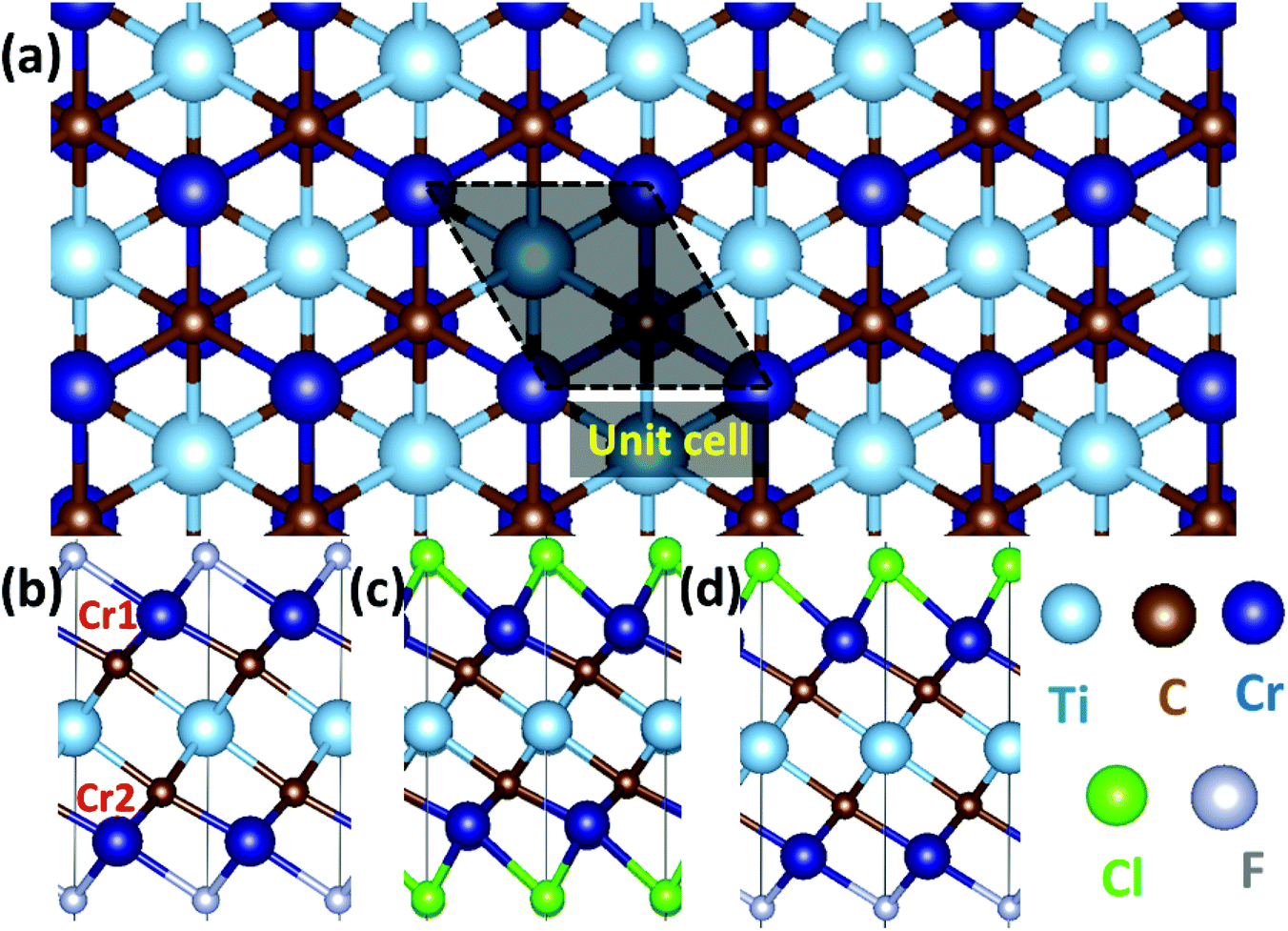
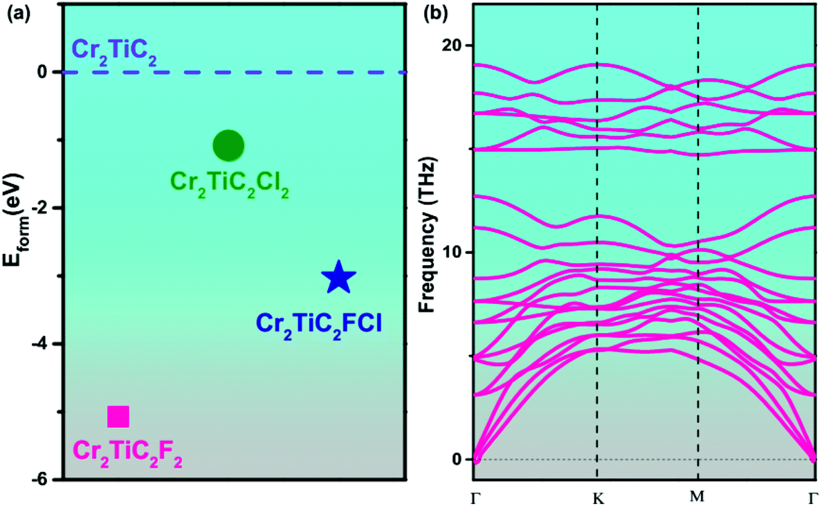
To explore this aforementioned concept further, we constructed Cr2TiC2FCl, as shown in Fig. 1d. The lattice constant of 2D Cr2TiC2FCl double MXenes is 3.10 Å, which is just between the lattice constants of the Cr2TiC2F2 and Cr2TiC2Cl2 monolayer. To evaluate the stability of Cr2TiCFCl monolayer, the formation energy, Eform, was calculated as follows:| | 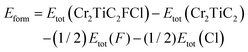 | (1) |
where Etot(Cr2TiC2) and Etot(Cr2TiC2FCl) stand for the total energies of pristine and functionalized MXenes, respectively. Energies of F2 and Cl2 in the gas phase were taken for the energies of Etot(F) and Etot (Cl), respectively. Similarly, the formation energy for the Cr2TiC2F2 and Cr2TiC2Cl2 monolayers also can be defined as follows:| | | Eform = Etot(Cr2TiC2T2) − Etot(Cr2TiC2) − Etot(T2) | (2) |
where T represents F/Cl atoms. The calculated formation energy for Cr2TiC2FCl, Cr2TiC2F2 and Cr2TiC2Cl2 are shown in Fig. 2a. It is clear that the formation energies for these structures are all negative and much lower than that of the pristine Cr2TiC2 monolayer, which indicates the formation of strong chemical bonds between the Cr atoms and F/Cl atoms. The formation energy for asymmetrically functionalized Cr2TiC2FCl is just in between the formation energies of the corresponding symmetrically functionalized Cr2TiC2F2 and Cr2TiC2Cl2. To confirm the dynamic stability of the Cr2TiC2FCl MXenes, we investigated the phonon spectra, as shown in Fig. 2b. We note that the phonon spectrum has quite small imaginary frequencies (∼0.12 THz) in the vicinity of the Γ point, suggesting that the monolayer Cr2TiC2FCl is unstable to long wavelength periodic distortions. A similar phenomenon is also observed in other 2D materials, such as the well-studied graphene.48,49 Such long-wavelength instability may induce ripples in the structure, but is not expected to significantly affect the overall structural stability of the 2D sheet.50,51 In principle, this instability can be suppressed by support from a proper substrate. These results indicate that the Cr2TiC2FCl MXenes monolayer is dynamically stable and can exist as a free-standing 2D monolayer.
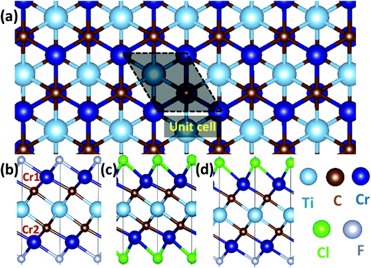 |
| | Fig. 1 (a) Top view for Cr2TiC2 double MXenes. The side view for (b) Cr2TiC2F2, (c) Cr2TiC2Cl2 and (d) Cr2TiC2FCl. The color scheme for Cr, C, Ti, F and Cl atoms is described in the figure. The Cr1 and Cr2 represent the Cl-bonded and F-bonded Cr atoms, respectively. | |
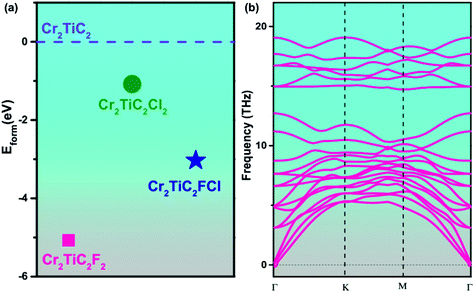 |
| | Fig. 2 (a) Formation energy (Eform) for symmetrical and asymmetrical double MXenes with respect to pristine Cr2TiC2. (b) Phonon dispersion curves for the Cr2TiC2FCl monolayer. | |
Next, we explored the electronic and magnetic properties of Cr2TiC2FCl. The FM states of the Cr2TiC2FCl monolayer have a total magnetic moment of 5.86μB (per unit cell), which is mainly contributed by Cr atoms. To determine the preferred magnetic ground state structures of the Cr2TiC2FCl sheets, the collinear FM, AFM-a, AFM-b and AFM-c states were considered, as shown in Fig. 3(a–d). It was found that the AFM-c magnetic configuration has the lowest energy, which was set as the reference energy. The FM, AFM-a, and AFM-b configurations have energies of 210 meV, 717 meV, 618 meV, respectively, with respect to the AFM-c configuration considering a 2 × 1 supercell. Moreover, including spin-orbital coupling, the non-collinear AFM (NCAFM) configuration with the 120° spin vectors and magnetic anisotropy were considered (see ESI†). These results clearly demonstrate that the AFM-c configuration of the Cr2TiC2FCl monolayer is the magnetic ground state with high magnetic stability. As shown in Fig. 3, the Cr layers in the upper-surface and lower-surface are separated by Ti2C with a vertical distance of 4.76 Å; therefore, the AFM-c ground state configuration has both intra-plane and inter-plane magnetic coupling.
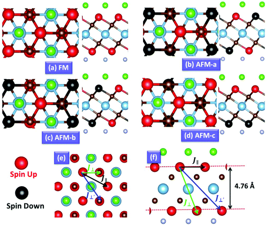 |
| | Fig. 3 The top and side views of possible magnetic configurations of the Cr2TiC2FCl MXene: FM (a), AFM-a (b), AFM-b (c), and AFM-c (d). Red and black balls represent Cr atoms with spin up and spin down electron configurations. The spin exchange parameter of the top view (e) and side view (f) for J‖, J⊥ and J⊥′ are also marked, respectively. | |
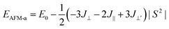
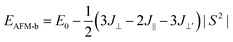
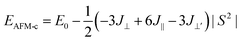
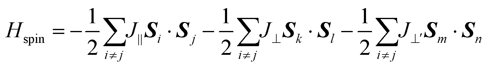
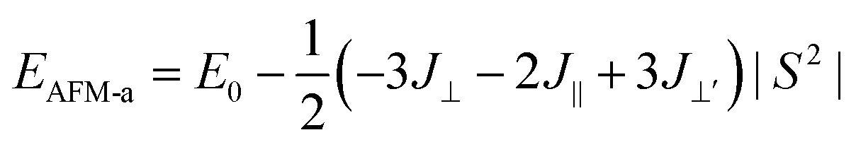
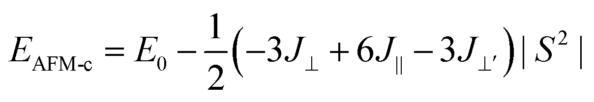
To describe quantitatively the magnetic properties of the Cr2TiC2FCl monolayer, the intra-plane magnetic exchange coupling constant (J||), and the inter-plane magnetic exchange coupling constant (J⊥ and J⊥′) were studied. The classical Heisenberg model with respect to J‖, J⊥ and J⊥′ exchange coupling parameters can be expressed as follows:
| |  | (3) |
where
S is the net magnetic moment (3
μB) at the Cr site i, and (
i,
j), (
k,
l) and (
m,
n) run over the nearest, next-nearest and next-next-nearest Cr atoms, respectively. By mapping the DFT total energies of the Cr
2TiC
2FCl of different magnetic structures (FM, AFM-a, AFM-b, and AFM-c) to the Heisenberg model, the exchange coupling parameters (
J‖,
J⊥ and
J⊥′) can be expressed by the following equations:
| |  | (4) |
| |  | (5) |
| |  | (6) |
| |  | (7) |
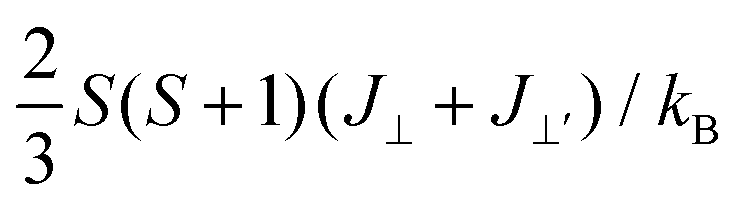
Thus, the magnetic exchange coupling parameters J‖, J⊥ and J⊥′ are 62.52 meV, −12.28 meV and −18.80 meV, respectively. These results demonstrate that the intra-plane coupling between the Cr atoms in the upper-surface and lower-surface has a strong ferromagnetic nature, while the inter-plane interaction maintains antiferromagnetic coupling. Furthermore, from the mean-field approximation, the Néel temperature can be evaluated as  ;52 thus, a high Néel temperature of 901 K is realized, suggesting potential applications for room-temperature spintronic devices.
3.3 Gate-controllable spin orientation
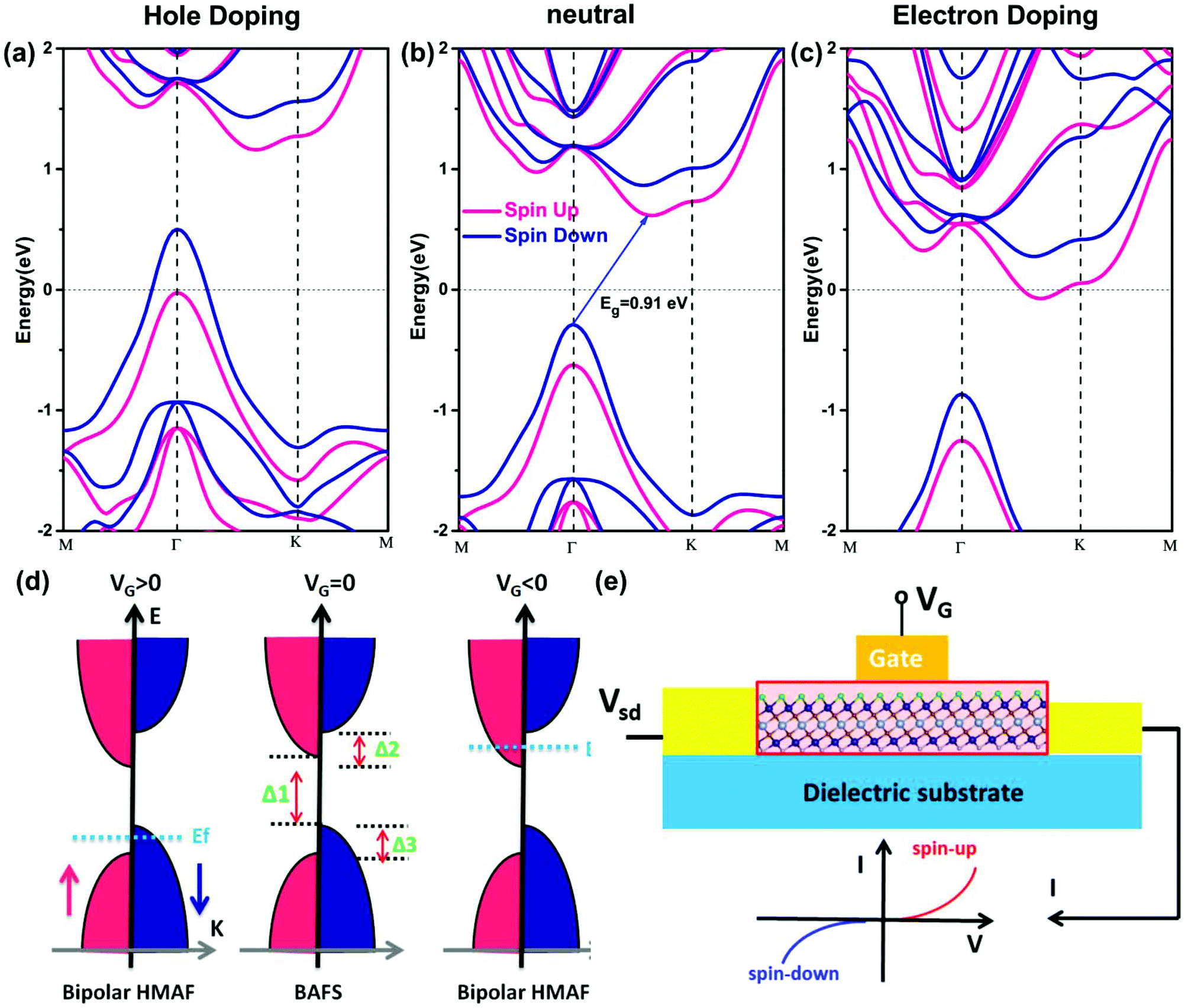
As AFM-c is the most stable magnetic state; in this section, we focus on its electronic and magnetic properties. The band structure of Cr2TiC2FCl shows that both the spin up and spin down states possess semiconducting features, with an indirect band gap of 0.91 eV, as shown in Fig. 4. Intriguingly, the valence band maximum (VBM) and the conduction band minimum (CBM) of Cr2TiC2FCl are derived from the opposite spin channels. Thus, the Cr2TiC2FCl sheet behaves as a novel bipolar antiferromagnetic semiconductor (BAFS). Unlike the bipolar magnetic semiconductor (BMS) proposed by Li et al.,53 Cr2TiC2FCl is a ferromagnetic material. Because of the opposite spin channels at the VBM and CBM, its spin-polarization direction can be controlled simply by applying a gate voltage. Recently, such gate-controllable magnetic states have been realized experimentally in few-layer Cr2Ge2Te6.54 Similar to the BMS materials, the BAFS feature of Cr2TiC2FCl also can be described by three energy gaps (Δ1, Δ2 and Δ3), as shown in Fig. 4d. The Δ1 gap is defined as a spin–flip gap with opposite spin polarization between the VBM and CBM, while (Δ1 + Δ2) and (Δ1 + Δ3) are defined as spin-conserved gaps. For practical applications of bipolar semiconductor, Δ1 should be small enough to moderately shift the Fermi level to spin-up/spin-down channels by the gate voltage. Moreover, Δ2 and Δ3 are expected to be large enough to guarantee the half-metallic gap. It is worth emphasizing that the values of Δ1, Δ2 and Δ3 are 0.91 eV, 0.31 eV, and 0.27 eV, respectively. These values fit the criteria of BMS very well, indicating that Cr2TiC2FCl sheet is a promising 2D material for AF spintronics applications.
 |
| | Fig. 4 Band structure for Cr2TiC2FCl double MXenes under gate voltage hole doping (a), neutral (b), and electron (c) with a carrier concentration of 0.1 electrons or holes per unit cell. The spin up and spin down channels are depicted in blue and pink, respectively. (d) The schematic plot of transformation between the bipolar HMAF and BAFS states under gate voltages of VG > 0, VG = 0, and VG < 0, respectively. Spin–flip gaps and spin-conserved gaps (Δ1, Δ2 and Δ3) are marked. (e) Schematic plot of antiferromagnetic spintronics device based on BAFS materials, together with the I–VG relationship under positive and negative gate voltage. The switching of the spin up and spin down current can be manipulated by the gate voltage. | |
As shown in Fig. 4a & c, there is a remarkable influence on the band structure of Cr2TiC2FCl for hole or electron doping. The doping electron and hole shift the Fermi level to different spin-polarized VBM and CBM regions, resulting in a tunable carrier spin orientation and transition from BAFS to HFAF. For low density electron doping, Cr2TiC2FCl changes from BMSAF to HMAF state with spin-down polarization, while a spin-up polarized HMAF state is obtained in the case of hole doping. Thus, completely spin-polarized currents with tunable spin orientation of the carriers and HMAF properties can be realized easily by a given doping type.
The novel BAFS materials combined with antiferromagnetic order and bipolar semiconducting character have potential applications for generating, manipulating, and detecting spin-polarized carriers in AF spintronics. Hence, in analogy to conventional semiconductor field effect transistors (FET), the gate voltage can switch the half-metallicity as well as control its spin polarized orientation. We briefly demonstrate a typical BAFS-based AF spin FET. As illustrated in Fig. 4(e), electron and hole doping was applied to tenably shift the Fermi level into the VB or CB in the BAFS materials. For instance, for hole doping, the Fermi level will shift into VB, resulting in a 100% spin-up polarized current (see Fig. 4e). Likewise, for electron doping, the Fermi level is conversely shifted into the CB; thus, a 100% spin-down polarized current is realized. Electron and hole doping can be realized experimentally by simply applying a gate voltage, as shown in Fig. 4d & e. The field-induced doping enables to control the spin polarized orientation and enhance the conductivity in BAFS materials, which will be promising for AF spintronics. Recently, gate-controllable electronic and magnetic properties in 2D magnets have been extensively reported.54–56 Particularly, the magnetic states of few-layer Cr2Ge2Te6 were controlled experimentally by gate voltage because of its bipolar magnetic semiconducting feature.54 When a practical gate voltage is applied, the electric field can induce charge transfer between 2D magnets and substrates, resulting in electron/hole doping. As shown in Fig. 4, the band structures were calculated by considering electron/hole doping. It is clear that doping shifts the Fermi level, and has a slight impact on the shape of the electronic band. However, for MXenes, the asymmetrical chemical adsorption induces a dipole in the z-direction. Our calculated dipole moment density is 0.034 eÅ (along z-axis direction) for monolayer Cr2TiC2FCl, which is comparable to that of other MXenes.57 When the real gate voltage is applied, it may enhance or suppress this dipole moment density and change the shape of the electronic band. To obtain a deeper understanding of the effects of the vertical gate voltage on the magnetic properties of MXenes, further comprehensive investigations are deserved.
3.4 The origin of BAFS
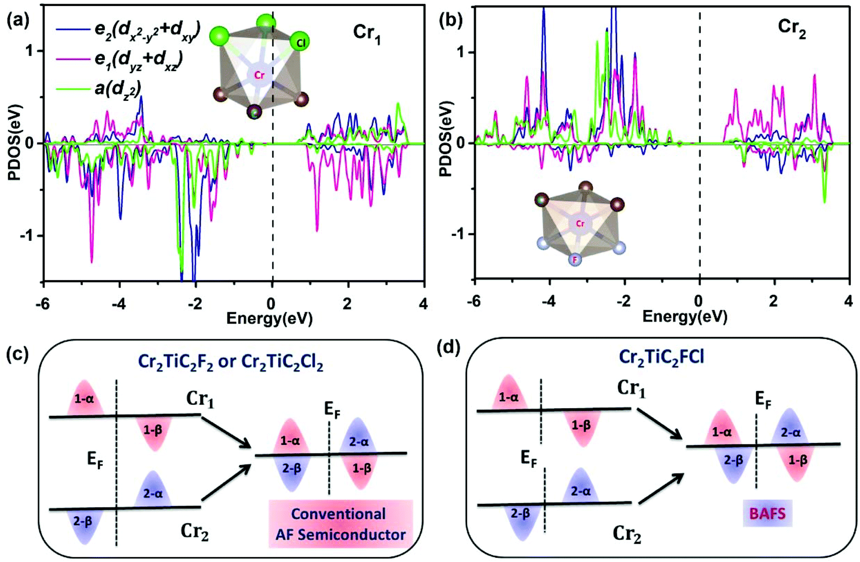
To gain insight into the fascinating electronic properties for Cr2TiC2FCl, the partial electronic density of states (PDOS) of the Cr1 (Cl-bonded Cr atom) and Cr2 (F-bonded Cr atom) atoms were recorded, as shown in Fig. 5. According to the D3d local symmetry of the crystal field on Cr1 and Cr2 atoms, the 3d orbitals split into a non-degenerate a (dz2) orbital and two 2-fold degenerate e1 (dxz/dyz) and e2 (dxy/dx2−y2) orbitals (the z axis is along the normal direction of the sheet). The VBM and CBM states of Cr2TiC2FCl are mainly derived from the Cr2-a and mixed Cr1-e1/Cr1-e2 states, respectively. According to Griffith's crystal field theory,58 the distribution of the d states of the TM ions reveal the crystal field splitting (Δcf) and exchange splitting (Δex) due to the crystal field interactions and on-site coulombic interaction, respectively.59,60 Clearly, the crystal field and exchange splitting of Cr1-d and Cr2-d are different, as shown in Fig. 5, because the Cr ions are located in a different chemical environment. Thus, the distinction of spin splitting between upper and lower Cr atoms is the dominant reason for the emergence of the BAFS feature in the Cr2TiC2FCl monolayer. Schematics of the Cr1 (upper Cr atoms) and Cr2 (lower Cr atom) spin exchange splitting in symmetrically and asymmetrically functionalized surfaces are shown in Fig. 5c & d. Although the individual Cr1 and Cr2 atoms are spin-polarized, they do not contribute to any net spin-polarization in the Cr2TiC2F2 and Cr2TiC2Cl2 system due to the equivalent chemical environment and the antiferromagnetic order. Nevertheless, for asymmetrical Cr2TiC2FCl MXenes, the different chemical environments in the upper and the lower surface induces a mismatch of d states for the Cr1 and Cr2 atoms, and consequently results in the BAFS feature.
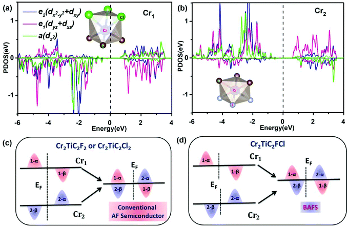 |
| | Fig. 5 PDOS of d states for Cl-bonded Cr1 (a) and F-bonded Cr2 (b) calculated for Cr2TiC2FCl. The insets show the local structure of the Cr atoms with F and Cl functionalization, respectively. The Fermi level is set to zero. Schematic diagrams of the Cr spin exchange splitting in symmetrically and asymmetrically functionalized surfaces are shown in (c) and (d), respectively. α and β represent the spin-up and spin down, respectively, and the Cr1 and Cr2 denote the upper and lower Cr atoms. | |
3.5 The mixed functionalization of double MXenes
The double MXenes Cr2TiC2FCl, with the perfectly asymmetrical F/Cl atom functionalization, is an ideal model. Generally, MXenes are obtained by exfoliation in a hydrogen fluoride solution where both surfaces have a mixed functionalization with H, OH and F atoms.61,62 It is therefore crucial to study the electronic properties for double MXenes with mixed functionalization. Next, we considered several typical mixed functionalization models (Cr2TiC2FxCl2−x, x = 0.25, 0.75, 1.25, 1.75) and calculated their magnetic and electronic properties, as shown in Fig. S3† and Fig. 6, respectively. These results show that the mixed functionalization double MXenes remain as a BAFS with interlayer AF ground states, as shown in Fig. 6. Thus, even an imperfect asymmetrical functionalization of Cr2TiC2 is sufficient to affect the chemical environment of the Cr atoms in the upper and lower surfaces to observe BAFS feature. In addition, the varying concentration of F/Cl on one of the surfaces provides an effective way to control the AF spin-polarization.
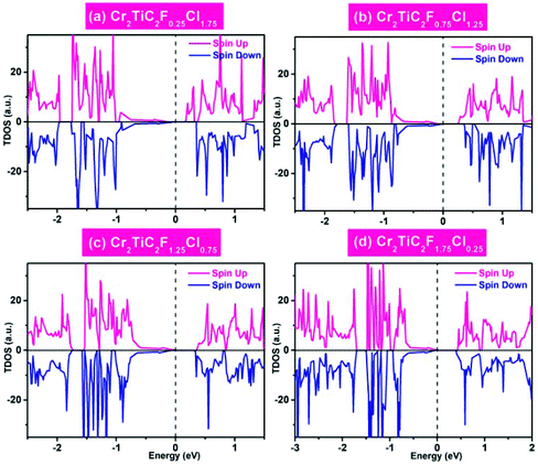 |
| | Fig. 6 DOS for various Cr2TiC2FxCl2−x systems, x = 0.25 (a), 0.75 (b), 1.25 (c), 1.75 (d). The pink and blue colors represent the spin up and spin down polarizations, respectively. The Fermi level is set to zero. | |
4. Summary
A new 2D bipolar antiferromagnetic semiconductor (BAFS) is reported for asymmetrical and mixed functionalization of Cr2TiC2 double MXenes using DFT at the HSE06 level. The valence and conduction bands in the BAFS materials are made up of opposite spin channels in a compensated AF order. We found that the application of electron and hole doping can easily manipulate the spin carrier orientation, leading to the transition from BAFS to half-metal antiferromagnets (HMAF), which could be realized experimentally via gate voltage. We also found that the BAFS characteristics are present even in Cr2TiC2FxCl2−x systems with mixed functionalization of the upper and lower surfaces. Our results presented herein open a new road for AF spintronics and the realization of AF spin field effect transistors.
Conflicts of interest
There are no conflicts to declare.
Acknowledgements
J. H., Q. D., and C. Z. acknowledge financial support provided by National Natural Science Foundation of China (Grant No. 11804041, 11804040 and 11804039).
References
- S. A. Wolf, D. D. Awschalom, R. A. Buhrman, J. M. Daughton, S. Von Molnar, M. L. Roukes, A. Y. Chtchelkanova and D. M. Treger, Science, 2001, 294, 1488–1495 CrossRef CAS PubMed.
- S. Yan, D. J. Choi, J. A. Burgess, S. Rolf-Pissarczyk and S. Loth, Nat. Nanotechnol., 2015, 10(1), 40–45 CrossRef CAS PubMed.
- L. Hu, H. Huang, Z. Wang, W. Jiang, X. Ni, Y. Zhou, V. Zielasek, M. G. Lagally, B. Huang and F. Liu, Phys. Rev. Lett., 2018, 121(6), 066401 CrossRef PubMed.
- W. B. Zhang, Q. Qu, P. Zhu and C. H. Lam, J. Mater. Chem. C, 2015, 3, 12457–12468 RSC.
- J. Liu, Q. Sun, Y. Kawazoe and P. Jena, Phys. Chem. Chem. Phys., 2016, 18, 8777–8784 RSC.
- J. He, S. Ma, P. Lyu and P. Nachtigall, J. Mater. Chem. C, 2016, 4, 2518–2526 RSC.
- J. He, X. Li, P. Lyu and P. Nachtigall, Nanoscale, 2017, 9(6), 2246–2252 RSC.
- C. Si, J. Zhou and Z. Sun, ACS Appl. Mater. Interfaces, 2015, 7, 17510–17515 CrossRef CAS PubMed.
- J. He, P. Lyu and P. Nachtigall, J. Mater. Chem. C, 2016, 4, 11143–11149 RSC.
- J. He, P. Lyu, L. Z. Sun, Á. M. García and P. Nachtigall, J. Mater. Chem. C, 2016, 4, 6500–6509 RSC.
- X. Li and J. Yang, J. Mater. Chem. C, 2014, 2, 7071–7076 RSC.
- H. L. Zhuang, Y. Xie, P. R. C. Kent and P. Ganesh, Phys. Rev. B: Condens. Matter Mater. Phys., 2015, 92, 035407 CrossRef.
- Q. Wu, Y. Zhang, Q. Zhou, J. Wang and X. C. Zeng, J. Phys. Chem. Lett., 2018, 9(15), 4260–4266 CrossRef CAS PubMed.
- J. He and S. Li, Comput. Mater. Sci., 2018, 152, 151–157 CrossRef CAS.
- B. Huang, G. Clark, E. Navarro-Moratalla, D. R. Klein, R. Cheng, K. L. Seyler, D. Zhong, E. Schmidgall, M. A. McGuire, D. H. Cobden, W. Yao, D. Xiao, P. Jarillo-Herrero and X. Xu, Nature, 2017, 546, 270 CrossRef CAS.
- C. Gong, L. Li, Z. Li, H. Ji, A. Stern, Y. Xia, T. Cao, W. Bao, C. Wang, Y. Wang and Z. Q. Qiu, Nature, 2017, 546, 265 CrossRef CAS PubMed.
- M. Bonilla, S. Kolekar, Y. Ma, H. C. Diaz, V. Kalappattil, R. Das, T. Eggers, H. R. Gutierrez, M. H. Phan and M. Batzill, Nat. Nanotechnol., 2018, 13, 289–293 CrossRef CAS PubMed.
- D. J. O'Hara, T. Zhu, A. H. Trout, A. S. Ahmed, Y. K. Luo, C. H. Lee, M. R. Brenner, S. Rajan, J. A. Gupta and D. W. McComb,
et al.
, Nano Lett., 2018, 18, 3125–3131 CrossRef PubMed.
- J. Liu, M. Shi, J. Lu and M. P. Anantram, Phys. Rev. B, 2018, 97, 054416 CrossRef.
- X. Li, X. Wu and J. Yang, J. Am. Chem. Soc., 2014, 136, 11065–11069 CrossRef CAS PubMed.
- S. Jiang, J. Shan and K. F. Mak, Nat. Mater., 2018, 17, 406–410 CrossRef CAS PubMed.
- S. Jiang, L. Li, Z. Wang, K. F. Mak and J. Shan, Nat. Nanotechnol., 2018, 13, 549–553 CrossRef CAS PubMed.
- P. Jiang, L. Li, Z. Liao, Y. X. Zhao and Z. Zhong, Nano Lett., 2018, 18(6), 3844–3849 CrossRef CAS PubMed.
- B. Huang, G. Clark, D. R. Klein, D. Mac Neill, E. Navarro-Moratalla, K. L. Seyler, N. Wilson, M. A. McGuire, D. H. Cobden, D. Xiao and W. Yao, Nat. Nanotechnol., 2018, 13, 544–548 CrossRef CAS PubMed.
- J. J. Zhang, L. Lin, Y. Zhang, M. Wu, B. I. Yakobson and S. Dong, J. Am. Chem. Soc., 2018, 140(30), 9768–9773 CrossRef CAS PubMed.
- C. Huang, Y. Du, H. Wu, H. Xiang, K. Deng and E. Kan, Phys. Rev. Lett., 2018, 120, 147601 CrossRef PubMed.
- D. Yang, W. Yao, Q. Chen, K. Peng, P. Jiang, X. Lu, C. Uher, T. Yang, G. Wang and X. Zhou, Chem. Mater., 2016, 28, 1611–1615 CrossRef CAS.
- D. Zhong,
et al.
, Sci. Adv., 2017, 3(5), e1603113 CrossRef PubMed.
- X. Hu, Adv. Mater., 2012, 24, 294–298 CrossRef CAS PubMed.
- T. Jungwirth, J. Sinova, A. Manchon, X. Marti, J. Wunderlich and C. Felser, Nat. Phys., 2018, 14, 200–203 Search PubMed.
- H. Van Leuken and R. A. De Groot, Phys. Rev. Lett., 1995, 74, 1171 CrossRef CAS PubMed.
- H. Kurt, K. Rode, P. Stamenov, M. Venkatesan, Y. C. Lau, E. Fonda and J. M. D. Coey, Phys. Rev. Lett., 2014, 112, 027201 CrossRef CAS PubMed.
- A. K. Nayak, M. Nicklas, S. Chadov, P. Khuntia, C. Shekhar, A. Kalache, M. Baenitz, Y. Skourski, V. K. Guduru, A. Puri and U. Zeitler, Nat. Mater., 2015, 14, 679–684 CrossRef CAS PubMed.
- H. Ai, X. Liu, B. Yang, X. Zhang and M. Zhao, J. Phys. Chem. C, 2018, 122(3), 1846–1851 CrossRef CAS.
- J. He, P. Zhou, N. Jiao, X. Chen, W. Lu and L. Z. Sun, RSC Adv., 2015, 5(58), 46640–46647 RSC.
- M. Naguib, M. Kurtoglu, V. Presser, J. Lu, J. Niu, M. Heon, L. Hultman, Y. Gogotsi and M. W. Barsoum, Adv. Mater., 2011, 23, 4248–4253 CrossRef CAS PubMed.
- M. Naguib, O. Mashtalir, J. Carle, V. Presser, J. Lu, L. Hultman, Y. Gogotsi and M. W. Barsoum, ACS Nano, 2012, 6, 1322–1331 CrossRef CAS.
- H. Kumar, N. C. Frey, L. Dong, B. Anasori, Y. Gogotsi and V. B. Shenoy, ACS Nano, 2017, 11, 7648–7655 CrossRef CAS PubMed.
- J. Yang, X. Zhou, X. Luo, S. Zhang and L. Chen, Appl. Phys. Lett., 2016, 109, 203109 CrossRef.
- G. Kresse and J. Hafner, Phys. Rev. B: Condens. Matter Mater. Phys., 1993, 47, 558 CrossRef CAS.
- G. Kresse and D. Joubert, Phys. Rev. B: Condens. Matter Mater. Phys., 1999, 59, 1758 CrossRef CAS.
- J. P. Perdew, K. Burke and M. Ernzerhof, Phys. Rev. Lett., 1996, 77, 3865 CrossRef CAS PubMed.
- S. L. Dudarev, G. A. Botton, S. Y. Savrasov, C. J. Humphreys and A. P. Sutton, Phys. Rev. B: Condens. Matter Mater. Phys., 1998, 57, 1505 CrossRef CAS.
- K. Parlinski, Z. Q. Li and Y. Kawazoe, Phys. Rev. Lett., 1997, 78, 4063 CrossRef CAS.
- A. Togo, F. Oba and I. Tanaka, Phys. Rev. B: Condens. Matter Mater. Phys., 2008, 78(13), 134106 CrossRef.
- F. Karlicky, K. Kumara Ramanatha Datta, M. Otyepka and R. Zboril, ACS Nano, 2013, 7, 6434–6464 CrossRef CAS PubMed.
- L. Zhang, J. Yu, M. Yang, Q. Xie, H. Peng and Z. Liu, Nat. Commun., 2013, 4, 1443 CrossRef PubMed.
- Z. W. Tan, J. S. Wang and C. K. Gan, Nano Lett., 2010, 11(1), 214–219 CrossRef PubMed.
- N. Mounet and N. Marzari, Phys. Rev. B: Condens. Matter Mater. Phys., 2005, 71(20), 205214 CrossRef.
- S. Cahangirov, M. Topsakal, E. Aktürk, H. Şahin and S. Ciraci, Phys. Rev. Lett., 2009, 102(23), 236804 CrossRef CAS PubMed.
- H. Şahin, S. Cahangirov, M. Topsakal, E. Bekaroglu, E. Akturk, R. T. Senger and S. Ciraci, Phys. Rev. B: Condens. Matter Mater. Phys., 2009, 80(15), 155453 CrossRef.
- M. Pajda, J. Kudrnovský, I. Turek, V. Drchal and P. Bruno, Phys. Rev. B: Condens. Matter Mater. Phys., 2001, 64, 174402 CrossRef.
- X. Li, X. Wu, Z. Li, J. Yang and J. G. Hou, Nanoscale, 2012, 4, 5680–5685 RSC.
- Z. Wang, T. Zhang, M. Ding, B. Dong, Y. Li, M. Chen, X. Li, J. Huang, H. Wang, X. Zhao and Y. Li, Nat. Nanotechnol., 2018, 13, 554–559 CrossRef CAS PubMed.
- Y. Deng,
et al.
, Nature, 2018, 563, 94–99 CrossRef CAS PubMed.
- B. Huang,
et al.
, Nat. Nanotechnol., 2018, 13, 544–548 CrossRef CAS PubMed.
- Y. Liu,
et al.
, J. Am. Chem. Soc., 2016, 138(49), 15853–15856 CrossRef CAS PubMed.
-
J. S. Griffith, Theory of transition-metal ions, Cambridge University Press, New York, 1961 Search PubMed.
- J. He, N. Jiao, C. Zhang, H. Xiao, X. Chen and L. Sun, J. Phys. Chem. C, 2014, 118(17), 8899–8906 CrossRef CAS.
- J. He, S. Y. Ma, P. Zhou, C. X. Zhang, C. He and L. Z. Sun, J. Phys. Chem. C, 2012, 116(50), 26313–26321 CrossRef CAS.
- X. Wang, X. Shen, Y. Gao, Z. Wang, R. Yu and L. Chen, J. Am. Chem. Soc., 2015, 137(7), 2715–2721 CrossRef CAS PubMed.
- M. A. Hope, A. C. Forse, K. J. Griffith, M. R. Lukatskaya, M. Ghidiu, Y. Gogotsi and C. P. Grey, Phys. Chem. Chem. Phys., 2016, 18, 5099 RSC.
Footnote |
| † Electronic supplementary information (ESI) available. See DOI: 10.1039/c8nr07692h |
|
| This journal is © The Royal Society of Chemistry 2019 |
Click here to see how this site uses Cookies. View our privacy policy here. 
 *ab,
Guangqian
Ding
*ab,
Guangqian
Ding


 ;52 thus, a high Néel temperature of 901 K is realized, suggesting potential applications for room-temperature spintronic devices.