
Transport and photogalvanic properties of covalent functionalized monolayer black phosphorus†
Cuicui
Sun
 ,
Yuxiu
Wang
,
Yingjie
Jiang
,
Zhao-Di
Yang
,
Guiling
Zhang
* and
Yangyang
Hu
*
,
Yuxiu
Wang
,
Yingjie
Jiang
,
Zhao-Di
Yang
,
Guiling
Zhang
* and
Yangyang
Hu
*
School of Materials Science and Engineering, Harbin University of Science and Technology, Harbin 150080, China. E-mail: guiling-002@163.com
First published on 21st November 2018
Abstract
Covalent functionalization is an efficient approach to modulate the nanoelectronic properties, advance the charge separation efficiency, and thus optimize the optoelectronic applications of nanomaterials. Here, the electronic structures, transport properties, and linear photogalvanic effects of two dimensional (2D) monolayer black phosphorus (MLBP) functionalized by PtCl2 groups, (PtCl2)n-MLBP (n = 1, 2, and 4) have been theoretically investigated using density functional theory (DFT), nonequilibrium Green's function (NEGF), and the Keldysh nonequilibrium Green's functions (KNEGF) methods. In the functionalized systems, the valence band maximum comes from the PtCl2 groups while the conduction band minimum originates from the MLBP. Such spatial charge separation hinders electron–hole recombination, suggesting MLBP-based 2D materials as promising candidates for solar cells. The MLBP-based device exhibits opposite responses for the transport properties and linear photogalvanic effects. The transport properties of MLBP along both the armchair and zigzag directions decrease after being grafted with PtCl2 groups. Moreover, the larger the grafting density n, the lower the conductivity. In comparison, the linear photogalvanic effects augment after functionalization, and this phenomenon is more significant with large n. Further, the photoresponse in the zigzag direction is larger by an order of magnitude than that in the armchair direction.
Introduction
Since the successful exfoliation of graphene in 2004,1 two dimensional (2D) nanomaterials have attracted intense research interest due to their unprecedented electronic and optical properties, such as large photoreactive contact area for optical absorption, tunable optoelectronic characteristics, relatively high carrier mobility and on–off current ratio, etc.2–4 Until now, various 2D nanomaterials have been obtained, but each possesses its own complement of favorable and unfavorable attributes. For instance, despite the high carrier mobility of graphene (reaches up to 106 cm2 V−1 s−1),5 the zero band gap6 limits its widespread application in optoelectronic devices. Theoretical calculation predicted that the electron and hole mobility of silicene is as high as 105![[thin space (1/6-em)]](https://www.rsc.org/images/entities/char_2009.gif) cm2 V−1 s−1 at room temperature,7 but preparation of silicene in experiments is relatively difficult,8–10 which greatly hinders its practical applications.11 In the case of MoS2, the on–off current ratio is large, the subthreshold swing is small and the band gap is extended,12–15 but the carrier mobility of MoS2 is relatively low.16 Therefore, searching for and designing new 2D materials with excellent photoelectric properties is still of great urgency in practical device research.
cm2 V−1 s−1 at room temperature,7 but preparation of silicene in experiments is relatively difficult,8–10 which greatly hinders its practical applications.11 In the case of MoS2, the on–off current ratio is large, the subthreshold swing is small and the band gap is extended,12–15 but the carrier mobility of MoS2 is relatively low.16 Therefore, searching for and designing new 2D materials with excellent photoelectric properties is still of great urgency in practical device research.
Monolayer black phosphorus (MLBP), an interesting and promising 2D elemental material,17,18 offers a major improvement in the performance of 2D nanomaterials. The device based on BP is promising as an electrophotonic detector from visible to infrared,19,20 even to the ultraviolet.21 A direct band gap makes it possible for MLBP to convert light and electricity directly without the participation of phonons under certain conditions, which is of great importance for improving the capability of devices such as solar cells.22–24 In addition to the characteristics mentioned above, MLBP possesses a high electron mobility of about 1000 cm2 V−1 s−1,25 and at the same time, its hole mobility reaches up to 105 cm2 V−1 s−1.26 All the above-mentioned features endow MLBP with fascinating properties and make it a competitor with other 2D nanomaterials, leading to it being a potential candidate for electronic devices and photovoltaic cell applications.27
In addition, functionalization is an effective way to further broaden the applications of 2D nanomaterials.28–30 To date, the photoelectric properties of MLBP can be modulated in a variety of ways, such as doping,31–33 stack layers,34,35 defect-modification,36 applying strain37 and external electric field,38etc. In particular, MLBP–metal interaction has drawn considerable attention in recent years on account of its relevance to the electrode-channel interface in MLBP-based nanoelectronic devices. It has been pointed out that the electronic structure and charge carrier type in MLBP can be tuned by metal adatoms forming strong interactions.39–43 Besides, functionalization can also enhance the structural stability of BP,30,44–47 which provides tremendous advantages over its 2D competitors.
Indeed, theoretical research shows that platinum (Pt) functionalization has been widely used to produce hybrid nanostructures with distinguishable photoelectric properties.31,39,43,48,49 Generally, Pt preferentially adopts planar four-coordination environments to form Pt[L2X2] complex (L and X = ligands),50–52 where Pt atoms lose valence electrons to the antibonding π* orbitals of the L and X ligands while L and X offer lone pair feedback to the empty orbitals of Pt.53–56 Experimentally, many Pt four-coordination complexes have been synthesized using various methods, such as Pt[P(C2H5)3]2C12,57–59 [Pt(NCNEt2)2(PPh3)2],60 PtX2(P(OMe)3)2 (X = Br, I),61 and Pt[C2H2(Ph)](SAr)(PPh3)2,62etc. Considering the enhanced performance that Pt brings to various nanomaterials, Pt-functionalized MLBP may present fascinating photoelectric properties for practical applications. Therefore, the transport and photogalvanic properties of the functionalized systems have been predicted in the present work, aiming to offer some clues for further efforts on the rational design of devices based on MLBP.
Results and discussions
Models and computational methods
Supercells containing 32 P atoms were constructed as 2 × 4 (x × y) by repeating the unit cell of MLBP twice along the x direction and four times along the y direction, as shown in Fig. 1. For the graft-functionalized systems, 1, 2, and 4 PtCl2 groups were selected to be grafted to the supercell to explore the effects of grafting density. Correspondingly, the functionalized structures studied are referred to as (PtCl2)n-MLBP (n = 1, 2, and 4) to simplify the description in the following discussions. The optimized supercell parameters of MLBP and (PtCl2)n-MLBP (n = 1, 2, and 4) are supplied in Table S1 of ESI.† For comparison, the electronic properties, transport properties, and linear photogalvanic effects of pure MLBP were also computed.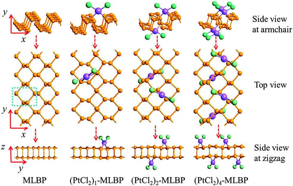 | ||
| Fig. 1 Optimized structures of infinite long MLBP and (PtCl2)n-MLBP (n = 1, 2, and 4). The structure in the blue dashed line represents a unit cell of MLBP. The yellow atom is P, the purple atom is Pt, and the green atom is Cl. | ||
To investigate the transport and linear photogalvanic effects, a two-probe device was constructed (as shown in Fig. 2). The left- and right-hand electrodes are Au with (100)-(9 × 3) surfaces which extend to a 25.95 Å × 8.65 Å plane. The distance of the interface between Au and MLBP has been optimized employing the Quasi-Newton method. The results show that the nearest P–Au distance is 2.33 Å, which is in the range of covalent interactions.63 The scatter region is composed of pure MLBP or (PtCl2)n-MLBP (n = 1, 2, and 4). Due to the existence of anisotropy in these systems, the scatter region was designed to be close to a square plane (26.05 Å (x direction) × 26.51 Å (y direction)). Such a scatter region was formed by repeating each optimized supercell 3 times in the armchair (x) direction and 2 times in the zigzag (y) direction. In this situation, we are able to investigate the transport and optical properties along the armchair, as well as the zigzag, direction only by rotating the scatter region by 90°, avoiding the impact of size. To facilitate description, the two-probe device using the armchair direction or zigzag direction as the transport direction is denoted as A-(PtCl2)n-MLBP or Z-(PtCl2)n-MLBP (n = 1, 2, and 4), respectively. Similarly, A-MLBP or Z-MLBP denotes the MLBP two-probe device. The scatter region is long enough to avoid electrode–electrode interaction. Transport current was computed by changing the applied bias voltage in steps of 0.2 V in the range −1.0 to 1.0 V.
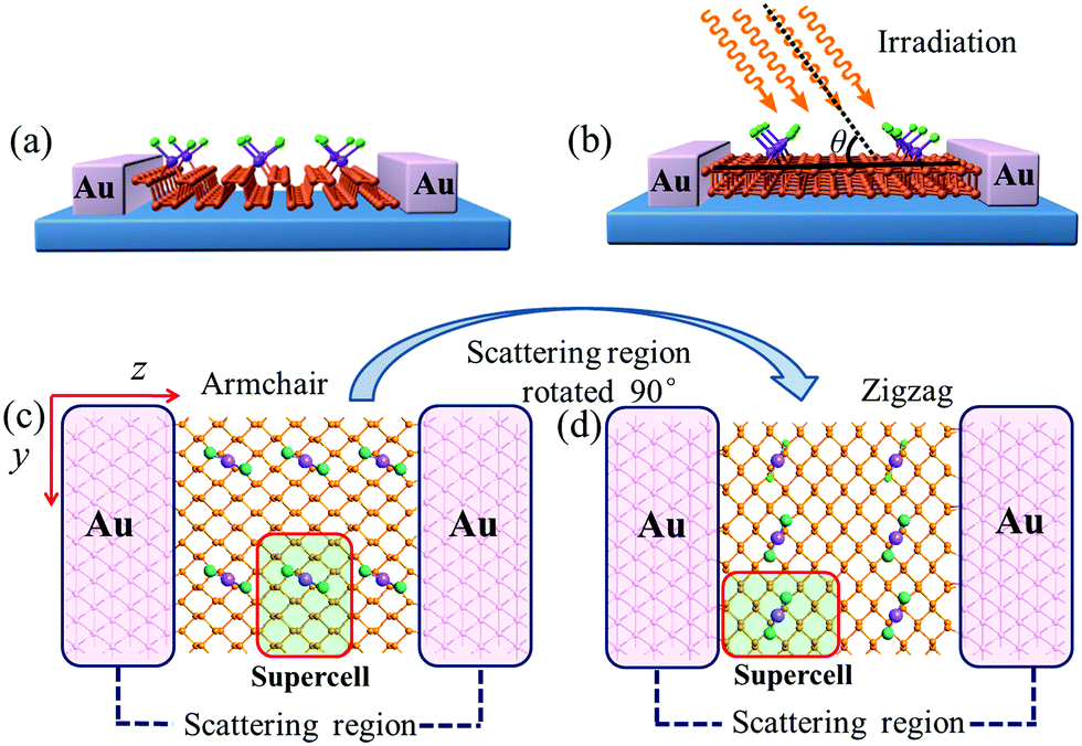 | ||
| Fig. 2 Exemplified two-probe devices by (PtCl2)1-MLBP. (a) Side view of A-(PtCl2)1-MLBP; (b) side view of Z-(PtCl2)1-MLBP; (c) top view of A-(PtCl2)1-MLBP; (d) top view of Z-(PtCl2)1-MLBP. Irradiation on the scatter regions of two-probe devices are schematically shown in (b). In order to investigate the grafting density effect on the transport properties, we replaced the supercell with the structure in Fig. 1. | ||
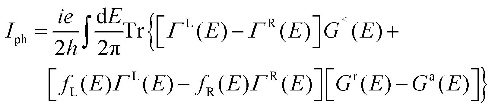
The computations for structural optimization of the infinitely large systems and the electrical transport properties of two-probe systems were implemented in the ab initio code package ATK64–66 on the basis of the combination of density functional theory (DFT) and the nonequilibrium Green's function (NEGF) methods. The exchange–correlation function was treated within the generalized gradient approximation (GGA).67 In addition, considering a non-zero magnetic moment may exist in our studied systems,53–56 the total density of states was calculated to make it clear. No obvious discrepancy between the spin up and the spin down states can be observed in our results, so we performed our calculations without polarization (see Fig. S1, ESI†). The on-site correlation effect among 5d electrons of the Pt atom was accounted for by using the SGGA+U scheme,66 where the parameter U–J was set to be 7.5 eV.68 A single-zeta (ζ) polarization (SZP) was used for all atoms. A (7 × 5 × 1) k-point in the Brillouin zone (x, y, z directions, respectively) was adopted and a 150 Ry cutoff energy was applied to describe the periodic wave function. The linear phase-coherent photocurrent was calculated with the Nanodcal69,70 package which carried out DFT within the Keldysh nonequilibrium Green's function (KNEGF). Standard norm-conserving nonlocal pseudopotentials were adopted to define the atomic cores, and a SZP linear combination of atomic orbital basis set was used to expand physical quantities. The photocurrent, Iph, could be obtained via the following formula71
 | (1) |
 | (2) |
Stability and geometry
In view of the puckered hexagonal structure of MLBP, there are 20 graft functionalized structures (see Table S2, ESI†): 2 for (PtCl2)1-MLBP, 10 for (PtCl2)2-MLBP, and 8 for (PtCl2)4-MLBP. All the considered structures were optimized and the values of total energies Etot are also listed in Table S2 (ESI†). For a given n, the functionalized structures with the largest absolute value of Etot are the most favorable ones. Therefore, we chose three of the most stable ones as the computational prototypes to investigate the electronic properties, transport properties, and linear photogalvanic effects (see Fig. 1). In addition, the adsorption energies, Ea, have been calculated for the selected systems. The Ea are defined as Ea = E(PtCl2)n–MLBP − EMLBP − nE(PtCl2), (n = 1, 2, and 4), where E(PtCl2)n–MLBP, EMLBP, and E(PtCl2) denote the total energies of the optimized functionalized systems, pristine MLBP, and PtCl2 in the unit cell, respectively. The Ea values of the three selected structures are −0.53, −1.06, and −2.55 eV for n = 1, 2, and 4, i.e., 0.53, 0.53, and 0.64 eV per PtCl2 group, respectively (as shown in Table 1). The relatively larger Ea means that there is a strong interaction between the PtCl2 group and MLBP. We also calculated the electron difference densities (the difference between the self-consistent valence charge density and the superposition of atomic valence density) for (PtCl2)n-MLBP (n = 1, 2, and 4) to visualize the interactions between MLBP and PtCl2, as shown in Fig. 3. Obvious charge transfers from the MLBP substrate to PtCl2 can be observed, indicating a strong coupling between them.| Species | E tot (eV) | E a (eV) | E exc (eV) | r outP–P (Å) | r inP–P (Å) | r Pt–P (Å) | r Pt–Cl (Å) | R Pt–Pt (Å) | R Cl–Cl (Å) |
|---|---|---|---|---|---|---|---|---|---|
| MLBP | −8449.61 | — | — | 2.244 | 2.224 | — | — | — | — |
| (PtCl2)1-MLBP | −10185.48 | −0.53 | 0.20 | 2.316 | 2.264 | 2.381 | 2.397 | — | — |
| (PtCl2)2-MLBP | −11921.35 | −1.06 | 0.17 | 2.335 | 2.265 | 2.388 | 2.399 | 6.314 | 7.917 |
| (PtCl2)4-MLBP | −15393.52 | −2.55 | 0.14 | 2.374 | 2.284 | 2.434 | 2.401 | 6.627 | 6.627 |
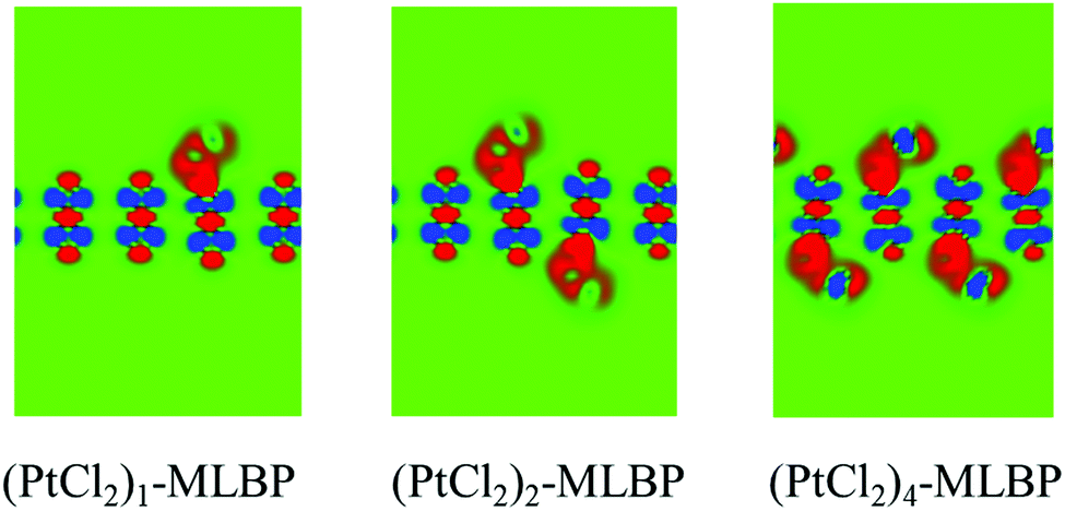 | ||
| Fig. 3 Computed electron difference densities of (PtCl2)1-MLBP, (PtCl2)2-MLBP, and (PtCl2)4-MLBP. The green region represents neutral and the red (blue) part represents obtaining (losing) electrons. | ||
MLBP has a layered structure consisting of double packed sublayers. Table 1 gives the geometric parameters of MLBP and (PtCl2)n-MLBP (n = 1, 2, and 4). From the data, each P atom is bound to three neighbouring atoms: one is out of the subplane at a distance of routP–P = 2.244 Å and the other two are in the subplane at a distance of rinP–P = 2.224 Å.72 The grafted PtCl2 groups prefer to locate over the furrow site rather than on the ridge position. A planar structure is formed in these (PtCl2)n-MLBP (n = 1, 2, and 4) complexes, a typical quadridentate structure for Pt. For (PtCl2)2-MLBP and (PtCl2)4-MLBP, the PtCl2 groups tend to distribute evenly on both surfaces of MLBP. The new-forming bonds of Pt–P weaken the neighboring P–P interactions, the routP–P and rinP–P are elongated to 2.316–2.374 Å and 2.264–2.284 Å, respectively. The Pt–P bond lengths rPt–P are 2.381–2.434 Å, in line with the general Pt–P chemical bond lengths (2.220–2.500 Å) reported in the literature.61,73 The values of Pt–Cl bond lengths rPt–Cl are in the range of 2.397–2.401 Å, also in accordance with literature reported values of 2.329–2.413 Å.74,75 The nearest Pt–Pt (RPt–Pt) and Cl–Cl (RCl–Cl) distances between two adjacent PtCl2 groups are up to 6.314–6.627 and 6.627–7.917 Å, respectively.
Bandstructure
First, we give the computed electronic properties based on pure MLBP for comparison (as shown in Fig. S2, ESI†). The valence band maximum (VBM, labeled as i, pink line) and the conduction band minimum (CBM, noted as ii, red line) of MLBP open a direct band gap about 0.85 eV at the Γ point closer to the 0.9 eV value reported before, showing a semi-conductive feature.26 After grafting of PtCl2 groups onto the MLBP surface, the properties of each isolated component may be preserved as well as new properties generated as a result of their combination.The band structures, projected density of states (PDOS), and the Kohn–Sham orbitals near the Fermi level (Ef) of the infinite large (PtCl2)n-MLBP (n = 1, 2, and 4) are shown in Fig. 4. In these functionalized systems, band i and band ii mainly preserve the VBM and CBM characteristics of the substrate MLBP, respectively. The i–ii band gaps are increased to 1.10, 1.09, and 1.18 eV for n = 1, 2, and 4, respectively, which is larger than that of pure MLBP (0.85 eV), indicating that grafting PtCl2 groups has a destructive effect on the conductivity of MLBP. We find that the PtCl2 groups introduce two kinds of impurity bands below the Ef: the higher one is close to the Ef and is composed of the Cl 3p states (green lines), while the lower one consists of the Pt 5d states (blue lines). The VBM i of MLBP is buried under the PtCl2 impurity bands and slightly hybridizes with Pt-5d/Cl-3p states. Moreover, with increasing the grafting density n, the VBM i of MLBP is shielded by more impurity bands due to the orbital interaction and reorganization. Usually, the Pt quadridentate compounds belong to inner-orbital complexes with a zero magnetic moment. However, the [Cl2P2] ligands generate an uneven ligand field, leading to a Jahn–Teller effect in (PtCl2)n-MLBP (n = 1, 2, and 4). Consequently, the degenerate orbitals are split, and thus the discrete feature of the PtCl2 impurity bands appears. The PtCl2 impurity bands show a localized and discrete character viewed from the combination of the band structure, PDOS, and Kohn–Sham orbitals. In this sense, the anchored PtCl2 behaves as a quantum-dot-like group. Clearly, (PtCl2)n-MLBP (n = 1, 2, and 4) systems bear spatially separated PtCl2 groups with localized and discrete features owing to the large separations between them, and electron tunneling through direct coupling of PtCl2 groups is minor.
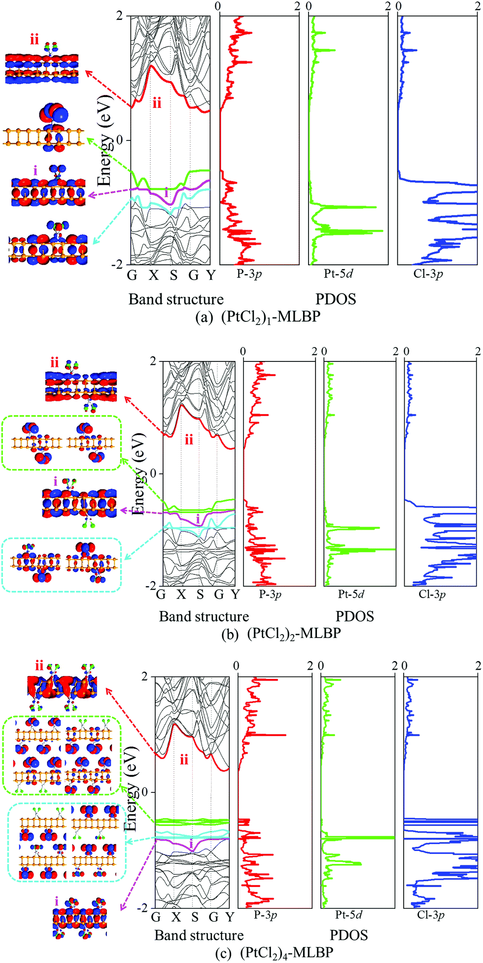 | ||
| Fig. 4 Computed band structures and PDOS for (a) (PtCl2)1-MLBP (b) (PtCl2)2-MLBP (c) (PtCl2)4-MLBP as well as the Kohn–Sham orbitals corresponding to the energy levels (highlighted with colored lines) near Ef at the G point. The iso-surface value is 0.02 (e Å−3). The coordination of each point was G(0, 0, 0), X(0.5, 0, 0), S(0.5, 0.5, 0), Y(0, 0.5, 0) and the Fermi level Ef is set to be zero. | ||
Notably, in the functionalized systems (PtCl2)n-MLBP (n = 1, 2, and 4), the impurity PtCl2 bands serve as the VBM while the MLBP ii band still behaves as the CBM, suggesting the possibility of a charge separation between the MLBP substrate and the PtCl2 groups. It is well known that spatial charge separation is a crucial phenomenon for solar energy conversion, as it lowers the probability of electron–hole recombination. The electron–hole interaction energies are around 0.2 eV, as shown by the calculated exciton binding energy Eexc of these functionalized systems (Table 1). In addition, the calculated absorption spectra indicate that they absorb light chiefly within the visible light range (Fig. S3 in ESI†). Therefore, the functionalized structures may find promising applications in solar cell design. Besides, the PtCl2 groups may have a two-fold effect on the transport property. On one hand, they offer extra valence electrons to be excited to the conduction bands to participate in transport, which is beneficial for enhancing the conductivity. On the other hand, the electron excitation of PtCl2 midgap levels leaves holes for trapping electrons from MLBP, that is, PtCl2 groups act as additional scattering centers which degrade the mobility of the charge carriers. From the analysis above, it is concluded that the PtCl2 groups exert an important effect on transport and optoelectronic properties, which will be further confirmed by the following discussions. It should be mentioned that the nearest distance between two adjacent PtCl2 in (PtCl2)2-MLBP is the RPt–Pt with the value of 6.314 Å and they locate on the top and bottom surfaces of MLBP, respectively, so the interactions between PtCl2 groups are negligible. For (PtCl2)4-MLBP, the nearest distance between two adjacent PtCl2 on the same surface is RPt–Pt or RCl–Cl with the value of 6.627 Å, the band structures and PDOS exhibit localized character of the PtCl2 groups suggesting their ignoring interactions.
Transport properties
To further investigate the effect of PtCl2 groups on the transport properties of (PtCl2)n-MLBP (n = 1, 2, and 4), we built two-probe devices by sandwiching a square scatter region of the studied system between two Au electrodes (as shown in Fig. 2). The transmissions along the armchair (A-(PtCl2)n-MLBP (n = 1, 2, and 4)) and zigzag (Z-(PtCl2)n-MLBP (n = 1, 2, and 4)) directions are both considered. The calculated current–voltage (I–V) curves for the two-probe systems are given in Fig. 5(a and b). Clearly, adding PtCl2 groups decreases the conductivity of the functionalized system regardless of the transport direction. When the bias voltage is over 0.6 V, the currents are ordered as MLBP > (PtCl2)1-MLBP > (PtCl2)2-MLBP > (PtCl2)4-MLBP, demonstrating that the trap effect of the PtCl2 groups plays a significant role in transporting electrons. However, the I–V curves showed that the currents for A-(PtCl2)1-MLBP at the [0.0 V, 0.6 V] window are higher than for pure A-MLBP. To explain this, we calculated the energy spectra for A-MLBP and A-(PtCl2)1-MLBP at a bias of 0.2, 0.4, 0.6, and 0.8 V, as shown in Fig. S4 (ESI†). Clearly, more energy levels appear in the bias window of A-(PtCl2)1-MLBP than of A-MLBP when the applied voltage is smaller than 0.6 V. However, the opposite is the case when the bias increases to 0.8 V, i.e., more energy levels are observed in the bias window of A-MLBP. This may be the main reason why the current of A-(PtCl2)1-MLBP is larger than that of pure MLBP when the voltage is smaller than 0.6 V. Additionally, the transport properties exhibit obvious anisotropy between the armchair and zigzag directions. The current in the armchair direction was larger than in the zigzag direction under a given voltage. For example, under −1.0 V bias voltage, A-(PtCl2)4-MLBP gives a current of −8.17 μA while Z-(PtCl2)4-MLBP presents a lower value of only −2.68 μA. | ||
| Fig. 5 Computed I–V curves for (a) A-MLBP and A-(PtCl2)n-MLBP (n = 1, 2, and 4), and (b) Z-MLBP and Z-(PtCl2)n-MLBP (n = 1, 2, and 4) two-probe devices. | ||
To give further insight into the transport properties upon grafting (PtCl2)n (n = 1, 2, and 4), the transmission spectra (TS) at 1.0 V were calculated (as given in Fig. 6). Usually, from the integral area of the bias window on the TS, the current at different bias can be obtained. The larger the integral area in the bias window, the higher the current. Here, the bias window refers to [−V/2, V/2]. Clearly, for both A-(PtCl2)n-MLBP and Z-(PtCl2)n-MLBP (n = 1, 2, and 4), the valence band resonant peaks in the bias window shrink gradually with increasing n. When n = 4, the valence band resonant peaks in the bias window almost disappear, confirming the trap effect of the PtCl2 groups. The conduction band resonant peaks in the bias window of A-(PtCl2)n-MLBP (n = 1, 2, and 4) are much larger than those of Z-(PtCl2)n-MLBP (n = 1, 2, and 4), and thereby the armchair direction gives a relatively higher conductivity than the zigzag direction, in line with the I–V curves. This feature can also be proved by the local density of state (LDOS) at Ef computed via the spectral density matrix ρ(E) = ρL(E) + ρR(E), where L/R denotes the contribution from the left/right electrode (see Fig. 7). The more states along the transport direction, the larger the conductance value. Obviously, the state of the scatter regions of both A-(PtCl2)n-MLBP (n = 1, 2, and 4) and Z-(PtCl2)n-MLBP (n = 1, 2, and 4) fade away when adding more PtCl2 groups, again indicating the blocking effect of PtCl2 groups on electron transport. Compared to A-(PtCl2)n-MLBP (n = 1, 2, and 4), the block phenomenon in Z-(PtCl2)n-MLBP (n = 1, 2, and 4) is more obvious, correlating well with the higher conductivity for the armchair direction than the zigzag direction.
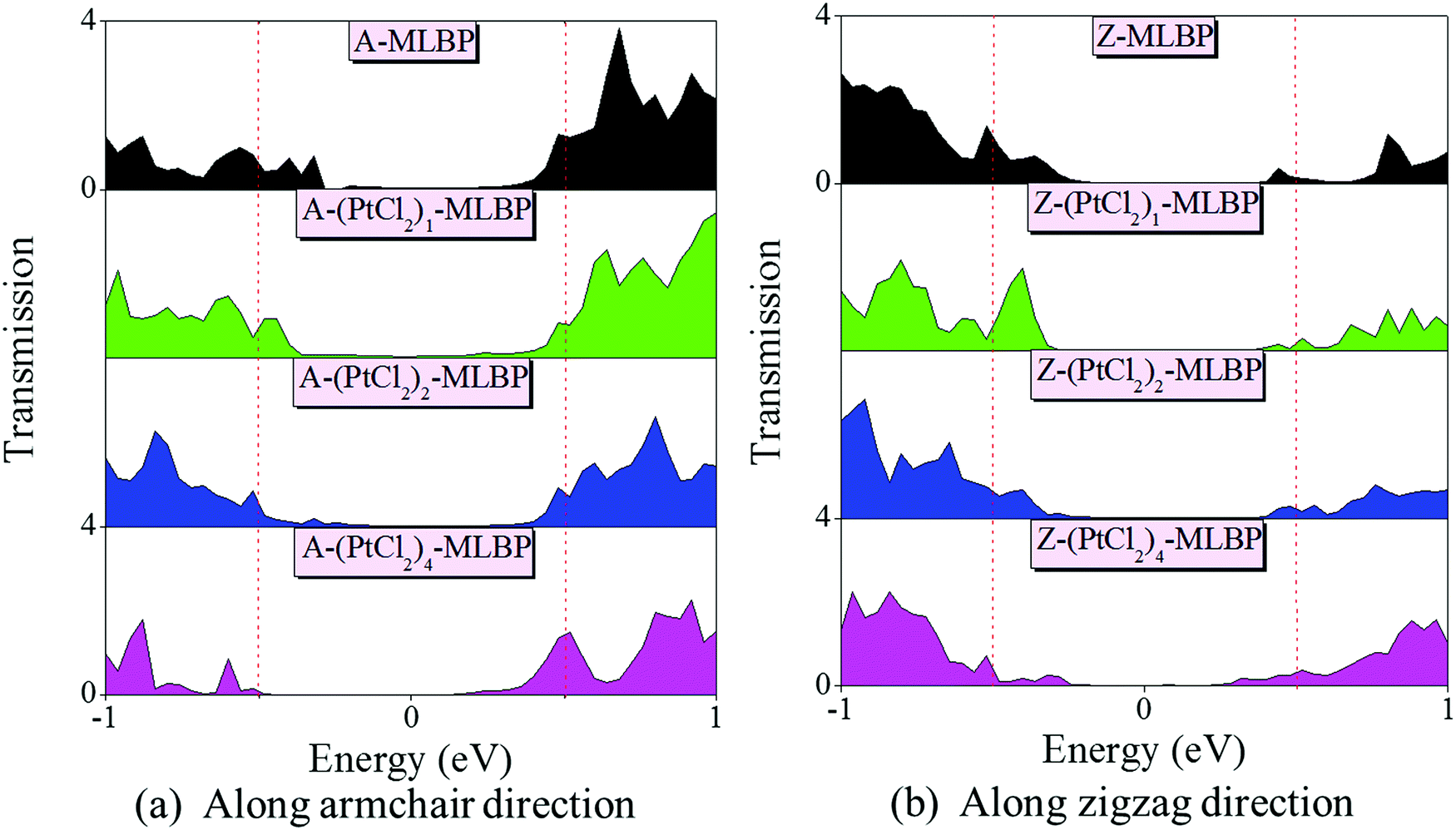 | ||
| Fig. 6 Transmission spectra of (a) A-MLBP and A-(PtCl2)n-MLBP (n = 1, 2, and 4), and (b) Z-MLBP and Z-(PtCl2)n-MLBP (n = 1, 2, and 4) two-probe devices at 1.0 V bias voltages. Red dashed lines indicate the bias window and the Fermi level Ef is set to be zero. | ||
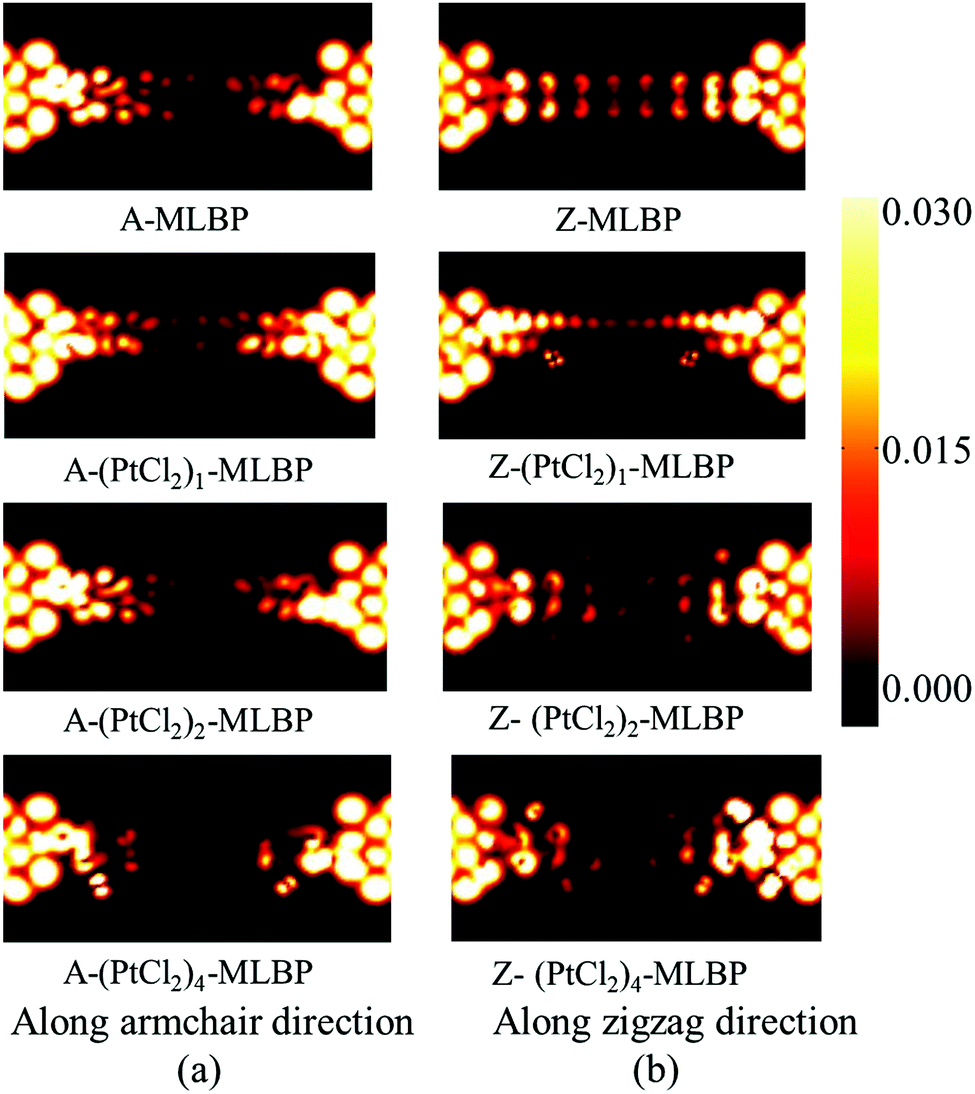 | ||
| Fig. 7 The LDOS at the Fermi energy Ef of (a) A-MLBP and A-(PtCl2)n-MLBP (n = 1, 2, and 4), and (b) Z-MLBP and Z-(PtCl2)n-MLBP (n = 1, 2, and 4) two-probe devices at 1.0 V bias voltages. | ||
Optoelectronic properties
For the purpose of investigating the linear photogalvanic effects of MLBP and (PtCl2)n-MLBP (n = 1, 2, and 4), we applied a linear polarized light on the whole scattering region based on the constructed two-probe devices (see Fig. 2(b)). The light is polarized in the y–z plane with the polarization vector forming an angle θ with respect to the z direction. The photocurrent along both the armchair and zigzag direction was calculated with respect to the anisotropy.76 Photoresponses were determined at different θ for photon energies ranging from 0 to 1.0 eV, with an interval of 0.1 eV.
Fig. 8 gives the photoresponses along both the armchair and zigzag directions of (PtCl2)n-MLBP (n = 1, 2, and 4) at photo energies of 0.7, 0.8, and 1.0 eV. The photoresponse curves exhibit sine or cosine shapes with θ since the photoresponses correlate directly to the sin2θ, cos2θ, and sin2θ components,77,78 which are determined by complicated factors such as the geometric symmetry and band structures. The sign of the photoresponse is determined by the summation of all activated electrons with different velocity distributions, so it varies with θ and applied photon energy. In other words, this should be attributed to the photo energy dependence of the Green's functions. It is noteworthy that the photoresponse is significantly enhanced by bonding PtCl2 groups. Regardless of whether in the armchair direction or the zigzag direction, the maximum photoresponses within the considered photon energies are sequenced as (PtCl2)4-MLBP > (PtCl2)2-MLBP > (PtCl2)1-MLBP > MLBP. This is in sharp contrast to the hindering effect of the PtCl2 groups in transporting electrons. Values for A-(PtCl2)4-MLBP and Z-(PtCl2)4-MLBP are up to 0.94 and 14.11 a02 per photon, respectively, 19 and 24 times larger than those of A-MLBP (0.05 a02 per photon) and Z-MLBP (0.58 a02 per photon), respectively. This is due to the fact that electrons can be excited easily by the light from the PtCl2 groups which can be demonstrated from the aforementioned band structures. Moreover, the photocurrent changes its sign with the polarization angle under illumination with linearly polarized light.
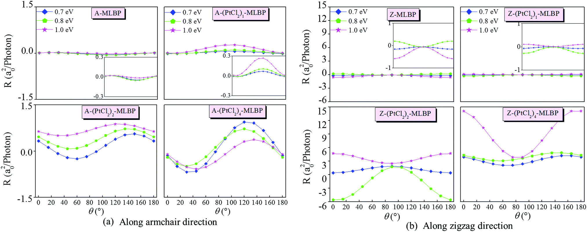 | ||
| Fig. 8 The calculated photoresponse for linear photogalvanic effects at different photon energies of (a) A-MLBP and A-(PtCl2)n-MLBP (n = 1, 2, and 4), and (b) Z-MLBP and Z-(PtCl2)n-MLBP (n = 1, 2, and 4). | ||
Fig. 9 shows the variation of maximum photoresponses with photo energies. Evidently, the (PtCl2)n-MLBP (n = 1, 2, and 4) composites give rise to photoresponse anisotropy: the zigzag direction (red) is about one order of magnitude larger than the armchair direction (black), contrary to the conductivity. All of these fascinating photoresponse properties make these new 2D materials especially attractive for optoelectronic devices.
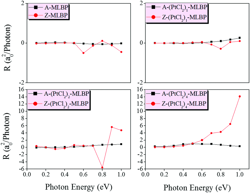 | ||
| Fig. 9 The calculated maximum photoresponse at the armchair and zigzag directions induced by linearly polarized light of MLBP and (PtCl2)n-MLBP (n = 1, 2, and 4). | ||
Conclusion
The electronic structures, transport properties, and linear photogalvanic effects of 2D MLBP-based nanomaterials, including (PtCl2)n-MLBP (n = 1, 2, and 4), are investigated employing DFT, NEGF, and KNEGF methods. Covalent functionalization of PtCl2 groups induces spatial charge separation between PtCl2 and MLBP, i.e., the VBM comes from the PtCl2 groups while the CBM originates from the MLBP. Such spatial charge separation hinders electron–hole recombination which is a crucial phenomenon for solar energy conversion. The PtCl2 groups can serve as energetically localized trap-states in the process of transporting electrons, which is the main reason for the decreasing conductivity of the functionalized systems (PtCl2)n-MLBP (n = 1, 2, and 4). The conductivity is ordered as (PtCl2)4-MLBP < (PtCl2)2-MLBP < (PtCl2)1-MLBP < MLBP. Electron transport is easier along the armchair direction than the zigzag direction. On the other hand, the photoresponse is significantly enhanced by bonding PtCl2 groups. The maximum photoresponses are sequenced as (PtCl2)4-MLBP > (PtCl2)2-MLBP > (PtCl2)1-MLBP > MLBP. The photoresponse in the zigzag direction is far superior to that in the armchair direction. All these features correlate well with the band structure predictions. These unique properties of (PtCl2)n-MLBP (n = 1, 2, and 4) make them especially attractive for both electronic and optoelectronic devices, in particular solar cell devices.Conflicts of interest
There are no conflicts to declare.Acknowledgements
This work was supported by National Natural Science Foundation of China (Grant No. 51473042), Nature Science Foundation of Heilongjiang Province of China (Grant No. B2018007), Harbin foundation for leaders of disciplines (Grant No. 2017RAXXJ002).Notes and references
- K. S. Novoselov, A. K. Geim, S. V. Morozov, D. Jiang, Y. Zhang, S. V. Dubonos, I. V. Grigorieva and A. A. Firsov, Science, 2004, 306, 666–669 CrossRef CAS PubMed.
- K. S. Novoselov, D. Jiang, F. Schedin, T. J. Booth, V. V. Khotkevich, S. V. Morozov and A. K. Geim, Proc. Natl. Acad. Sci. U. S. A., 2005, 102, 10451–10453 CrossRef CAS PubMed.
- M. Osada and T. Sasaki, Adv. Mater., 2012, 43, 210–228 CrossRef PubMed.
- C. Tan, X. Cao, X. J. Wu, Q. He, J. Yang, X. Zhang, J. Chen, W. Zhao, S. Han, G. H. Nam, M. Sindoro and H. Zhang, Chem. Rev., 2017, 117, 6225–6331 CrossRef CAS PubMed.
- A. K. Geim and K. S. Novoselov, Nat. Mater., 2007, 6, 183–191 CrossRef CAS PubMed.
- A. H. Castro Neto, F. Guinea, N. M. R. Peres, K. S. Novoselov and A. K. Geim, Rev. Mod. Phys., 2009, 81, 109–162 CrossRef CAS.
- Z. G. Shao, X. S. Ye, L. Yang and G. L. Wang, J. Appl. Phys., 2013, 114, 093712 CrossRef.
- L. Meng, Y. Wang, L. Zhang, S. Du, R. Wu, L. Li, Y. Zhang, G. Li, H. Zhou, W. A. Hofer and H. J. Gao, Nano Lett., 2013, 13, 685–690 CrossRef CAS PubMed.
- D. Chiappe, C. Grazianetti, G. Tallarida, M. Fanciulli and A. Molle, Adv. Mater., 2012, 24, 5088–5093 CrossRef CAS PubMed.
- C. L. Lin, R. Arafune, K. Kawahara, N. Tsukahara, E. Minamitani, Y. Kim, N. Takagi and M. Kawai, Appl. Phys. Express, 2012, 5, 045802 CrossRef.
- A. Molle, C. Grazianetti, D. Chiappe, E. Cinquanta, E. Cianci, G. Tallarida and M. Fanciulli, Adv. Funct. Mater., 2013, 23, 4340–4344 CrossRef CAS.
- B. Radisavljevic, A. Radenovic, J. Brivio, V. Giacometti and A. Kis, Nat. Nanotechnol., 2011, 6, 147–150 CrossRef CAS PubMed.
- G. Fiori, F. Bonaccorso, G. Iannaccone, T. Palacios, D. Neumaier, A. Seabaugh, S. K. Banerjee and L. Colombo, Nat. Nanotechnol., 2014, 9, 768–779 CrossRef CAS PubMed.
- G. Fiori, B. N. Szafranek, G. Iannaccone and D. Neumaier, Appl. Phys. Lett., 2013, 103, 233509 CrossRef.
- S. Kataria, S. Wagner, T. Cusati, A. Fortunelli, G. Iannaccone, H. Pandey, G. Fiori and M. C. Lemme, Adv. Mater. Interfaces, 2017, 4, 1700031 CrossRef.
- R. Fivaz and E. Mooser, Phys. Rev., 1967, 163, 743–755 CrossRef CAS.
- F. W. Han, W. Xu, L. L. Li, C. Zhang, H. M. Dong and F. M. Peeters, Phys. Rev. B: Condens. Matter Mater. Phys., 2017, 95, 115436 CrossRef.
- L. Li, Y. Yu, G. J. Ye, Q. Ge, X. Ou, H. Wu, D. Feng, X. H. Chen and Y. Zhang, Nat. Nanotechnol., 2014, 9, 372–378 CrossRef CAS PubMed.
- K. Wang, B. M. Szydłowska, G. Wang, X. Zhang, J. J. Wang, J. J. Magan, L. Zhang, J. N. Coleman, J. Wang and W. J. Blau, ACS Nano, 2016, 10, 6923–6932 CrossRef CAS PubMed.
- S. B. Lu, L. L. Miao, Z. N. Guo, X. Qi, H. Zhao, S. C. Wen, D. Y. Tang and D. Y. Fan, Opt. Express, 2015, 23, 11183–11194 CrossRef CAS PubMed.
- J. Wu, G. K. W. Koon, D. Xiang, C. Han, C. T. Toh, E. S. Kulkarni, I. Verzhbitskiy, A. Carvalho, A. S. Rodin, S. P. Koenig, G. Eda, W. Chen, A. H. Castro Neto and B. Özyilmaz, ACS Nano, 2015, 9, 8070–8077 CrossRef CAS PubMed.
- V. D. Ganesan, J. Linghu, C. Zhang, Y. P. Feng and L. Shen, Appl. Phys. Lett., 2016, 108, 122105 CrossRef.
- L. Bai, L. Sun, Y. Wang, Z. Liu, Q. Gao, H. Xiang, H. Xie and Y. Zhao, J. Mater. Chem. A, 2017, 5, 8280–8286 RSC.
- W. Hu, L. Lin, C. Yang, J. Dai and J. Yang, Nano Lett., 2016, 16, 1675–1682 CrossRef CAS PubMed.
- S. J. R. Tan, I. Abdelwahab, L. Chu, S. M. Poh, Y. Liu, J. Lu, W. Chen and K. P. Loh, Adv. Mater., 2018, 30, 1704619 CrossRef PubMed.
- H. Liu, A. T. Neal, Z. Zhu, D. Tomanec and P. D. Ye, ACS Nano, 2014, 8, 4033–4041 CrossRef CAS PubMed.
- P. Chen, N. Li, X. Chen, W. J. Ong and X. Zhao, 2D Mater., 2017, 5, 014002 CrossRef.
- Y. Guo and J. Robertson, Microelectron. Eng., 2017, 178, 108–111 CrossRef CAS.
- M. Xie, S. Zhang, B. Cai, Y. Huang, Y. Zou, B. Guo, Y. Gu and H. Zeng, Nano Energy, 2016, 28, 433–439 CrossRef CAS.
- Y. Zhao, H. Wang, H. Huang, Q. Xiao, Y. Xu, Z. Guo, H. Xie, J. Shao, Z. Sun, W. Han, X. F. Yu, P. Li and P. K. Chu, Angew. Chem., Int. Ed., 2016, 55, 5003–5007 CrossRef CAS PubMed.
- N. Suvansinpan, F. Hussain, G. Zhang, C. H. Chiu, Y. Cai and Y. Zhang, Nanotechnol., 2016, 27, 065708 CrossRef PubMed.
- I. Khan and J. Hong, New J. Phys., 2015, 17, 023056 CrossRef.
- G. Wang, R. Pandey and S. P. Karna, Appl. Phys. Lett., 2015, 106, 173104 CrossRef.
- J. Pang, A. Bachmatiuk, Y. Yin, T. Barbara, L. Zhao, L. Fu, R. G. Mendes, T. Gemming, Z. Liu and M. H. Rummeli, Adv. Energy Mater., 2018, 8, 1702093 CrossRef.
- J. Dai and X. C. Zeng, J. Phys. Chem. Lett., 2014, 5, 1289–1293 CrossRef CAS PubMed.
- M. U. Farooq, A. Hashmi and J. Hong, Sci. Rep., 2015, 5, 12482(1)–12482(11) Search PubMed.
- Z. Xie, L. Hui, J. Wang, G. Zhu, Z. Chen and C. Li, Comput. Mater. Sci., 2018, 144, 304–314 CrossRef CAS.
- S. P. Koenig, R. A. Doganov, H. Schmidt, A. H. Castro Neto and B. Oezyilmaz, Appl. Phys. Lett., 2014, 104, 10451(1)–10451(12) CrossRef.
- X. Wang, C. Tang, W. Zhu, X. Zhou, Q. Zhou and C. Chen, J. Phys. Chem. C, 2018, 122, 9654–9662 CrossRef CAS.
- A. Hashmi and J. Hong, J. Phys. Chem. C, 2015, 119, 9198–9204 CrossRef CAS.
- S. P. Koenig, R. A. Doganov, L. Seixas, A. Carvalho, J. Y. Tan, K. Watanabe, T. Taniguchi, N. Yakovlev, A. H. Castro Neto and B. Özyilmaz, Nano Lett., 2016, 16, 2145–2551 CrossRef CAS PubMed.
- X. Sun and Z. Wang, Appl. Surf. Sci., 2018, 427, 189–197 CrossRef CAS.
- P. Rastogi, S. Kumar, S. Bhowmick, A. Agarwal and Y. S. Chauhan, IETE J. Res., 2015, 63, 205–215 CrossRef.
- G. Abellán, V. Lloret, U. Mundloch, M. Marcia, C. Neiss, A. Görling, M. Varela, F. Hauke and A. Hirsch, Angew. Chem., 2016, 128, 14777–14782 CrossRef.
- C. R. Ryder, J. D. Wood, S. A. Wells, Y. Yang, D. Jariwala, T. J. Marks, G. C. Schatz and M. C. Hersam, Nat. Chem., 2016, 8, 597–602 CrossRef CAS PubMed.
- Z. Sofer, J. Luxa, D. Bouša, D. Sedmidubský, P. Lazar, T. Hartman, H. Hardtdegen and M. Pumera, Angew. Chem., 2017, 129, 10023–10028 CrossRef.
- Q. Li, Q. Zhou, X. Niu, Y. Zhao, Q. Chen and J. Wang, J. Phys. Chem. Lett., 2016, 7, 4540–4546 CrossRef CAS PubMed.
- S. Y. Cho, H. J. Koh, H. W. Yoo and H. Jung, Chem. Mater., 2017, 29, 7197–7205 CrossRef CAS.
- T. Hu and J. Hong, J. Phys. Chem. C, 2015, 119, 8199–8207 CrossRef CAS.
- Q. Laura de, B. B. Eike, M. Wolfgang, C. B. James, B. P. Thomas, M. M. A. José, H. Frank and A. G. John, J. Am. Chem. Soc., 2007, 129, 8296–8309 CrossRef PubMed.
- A. Arias, J. Forniés, C. Fortuño and A. Martin, Inorg. Chem., 2012, 51, 12682–12696 CrossRef CAS PubMed.
- A. Arias, J. Forniés, C. Fortuño, S. Ibanez and A. Martin, Inorg. Chem., 2013, 52, 11398–11408 CrossRef CAS PubMed.
- V. M. Miskowski, V. H. Houlding, C. M. Che and Y. Wang, Inorg. Chem., 1993, 32, 2518–2524 CrossRef CAS.
- D. S. Martin Jr, M. A. Tucker and A. J. Kassman, Inorg. Chem., 1965, 4, 1682–1689 CrossRef.
- L. G. Vanquickenborne and A. Ceulemans, Inorg. Chem., 1981, 20, 796–800 CrossRef CAS.
- S. S. Zumdahl and R. S. Drago, J. Am. Chem. Soc., 1968, 90, 6669–6675 CrossRef CAS.
- U. Belluco, M. Martelli and A. Orio, Inorg. Chem., 1966, 5, 582–586 CrossRef CAS.
- U. Belluco, P. Rigo, M. Graziani and R. Ettorre, Inorg. Chem., 1966, 5, 1125–1127 CrossRef CAS.
- G. G. Messmer and E. L. Amma, Inorg. Chem., 1966, 5, 1775–1781 CrossRef CAS.
- C. M. P. Ferreira, M. F. C. Guedes da Silva, J. J. R. Fraústo da Silva, A. J. L. Pombeiro, V. Y. Kukushkin and R. A. Michelin, Inorg. Chem., 2001, 40, 1134–1142 CrossRef CAS PubMed.
- P. G. Waddell, A. M. Slawin and J. D. Woollins, Dalton T., 2010, 39, 8620–8625 CAS.
- A. Ohtaka, H. Kuniyasu, M. Kinomoto and H. Kurosawa, J. Am. Chem. Soc., 2002, 124, 14324–14325 CrossRef CAS PubMed.
- R. E. Bachman and H. Schmidbaur, Inorg. Chem., 1996, 35, 1399–1401 CrossRef CAS PubMed.
- J. Taylor, H. Guo and J. Wang, Phys. Rev. B: Condens. Matter Mater. Phys., 2001, 63, 245407 CrossRef.
- M. Brandbyge, J. L. Mozos, P. Ordejon, J. Taylor and K. Stokbro, Phys. Rev. B: Condens. Matter Mater. Phys., 2002, 65, 165401 CrossRef.
- ATK, Version 13.8, atomistix a/s, 2013, http://www.quantumwise.com Search PubMed.
- J. P. Perdew, K. Burke and M. Ernzerhof, Phys. Rev. Lett., 1996, 77, 3865–3868 CrossRef CAS PubMed.
- Y. Yang, O. Sugino and T. Ohno, AIP Adv., 2012, 2, 022172 CrossRef.
- NanoDcal quantum transport package, http://nanoacademic.ca.
- D. Waldron, P. Haney, B. Larade, A. MacDonald and H. Guo, Phys. Rev. Lett., 2006, 96, 166804 CrossRef PubMed.
- J. Chen, Y. Hu and H. Guo, Phys. Rev. B: Condens. Matter Mater. Phys., 2012, 85, 155441 CrossRef.
- T. Takahashi, H. Tokailin, S. Suzuki, T. Sagawa and I. Shirotani, J. Phys. C: Solid State Phys., 1985, 18, 825–836 CrossRef CAS.
- N. Ainara, E. Stefan, A. J. Naseralla, N. P. Robin, A. M. Stuart, E. M. John and C. W. Adrian, J. Am. Chem. Soc., 2008, 130, 15499–15511 CrossRef PubMed.
- E. Alonso, J. Forniés, C. Fortuño, A. Lledós, A. Martín and A. Nova, Inorg. Chem., 2009, 48, 7679–7690 CrossRef CAS PubMed.
- P. Mastrorilli, C. F. Nobile, M. Latronico, V. Gallo, U. Englert, F. P. Fanizzi and O. Sciacovelli, Inorg. Chem., 2005, 44, 9097–9104 CrossRef CAS PubMed.
- T. Hong, B. Chamlagain, W. Lin, H. J. Chuang, M. Pan, Z. Zhou and Y. Q. Xu, Nanoscale, 2014, 6, 8978–8983 RSC.
- Y. Xie, L. Zhang, Y. Zhu, L. Liu and H. Guo, Nanotechnol., 2015, 26, 455202 CrossRef PubMed.
- S. Li, T. Wang, X. Chen, W. Lu, Y. Xie and Y. Hu, Nanoscale, 2018, 10, 7694–7701 RSC.
Footnote |
| † Electronic supplementary information (ESI) available. See DOI: 10.1039/c8nj04701d |
| This journal is © The Royal Society of Chemistry and the Centre National de la Recherche Scientifique 2019 |