
Surface-enhanced Raman scattering (SERS) as a probe for detection of charge-transfer between TiO2 and CdS nanoparticles†
Lin
Guo
,
Xiaolei
Zhang
,
Peng
Li
,
Rui
Han
,
Yawen
Liu
,
Xiaoxia
Han
 and
Bing
Zhao
*
and
Bing
Zhao
*
State Key Laboratory of Supramolecular Structure and Materials, Jilin University, Changchun 130012, People's Republic of China. E-mail: zhaob@mail.jlu.edu.cn; Fax: +86-431-85193421; Tel: +86-431-85168473
First published on 20th November 2018
Abstract
Charge-transfer processes of coupled semiconductor nanoparticles play an essential role in many application fields of semiconductors. It has been difficult to characterize the charge-transfer process between two semiconductor nanoparticles. Herein, we propose a new analytical tool with the chemical mechanism of Surface-Enhanced Raman Scattering (SERS) to provide information about the charge-transfer process in coupled semiconductor nanoparticle systems. In this work, two assemblies (namely, TiO2–MBA–CdS and CdS–MBA–TiO2) have been fabricated as models to explore the charge-transfer process between TiO2 and CdS nanoparticles by SERS. 4-MBA works as both the linker of these two semiconductors and the probe of SERS to reveal the charge-transfer process. Under excitations at 633 and 785 nm, which are far from the surface plasmon resonance of the CdS and TiO2 nanoparticles in the assemblies, there are some obvious changes in the peak intensities and peak shifts in the SERS spectra after introducing CdS to the TiO2/MBA system and TiO2 to the CdS/MBA system. The differences of the peak intensities in the TiO2–MBA–CdS and CdS–MBA–TiO2 assemblies show different charge-transfer processes. We have found that the dipole moment of a MBA molecule greatly influences the charge-transfer process between the TiO2 and CdS nanoparticles.
Introduction
Coupled semiconductor–semiconductor, and coupled semiconductor–molecule structures play important parts in solar cells1–3 and photocatalysis.4–6 Interparticle electron transfer between dissimilar semiconductor particles is an ongoing research topic. Part of the motivation for such studies is to enhance charge separation and an attempt to increase the lifetime of charge carriers, thereby improving the conversion efficiency of solar cells and the photocatalytic efficiency of various catalytic reactions. To enrich practical applications based on these coupled semiconductor–semiconductor and coupled semiconductor–molecule structures, many efforts have been made to study the feasible charge-transfer process involved. Hyun et al.7 reported the injection of photoexcited electrons from colloidal PbS into TiO2 nanoparticles for sensitizing solar cells. Bessekhouad et al.8 used CdS/TiO2 and Bi2S3/TiO2 to analyze the charge-transfer mechanism in the photocatalytic degradation of organic pollutants. Lee et al.9 investigated the electronic states that occur between N719 and TiO2 surfaces in dye-sensitized solar cells. However, it is difficult to observe the charge-transfer process between micro and nanoscale particles especially when the particles are less than 10 nm.It is a good choice that the process of photoelectric reaction reflected through the optical phenomenon or spectrum, and SERS provide such a way. The chemical enhancement mechanism (CM)10–13 of SERS involves a charge-transfer process between the substrate and the adsorbate. Typically, chemical enhancement is a resonance Raman-like process, which is sensitive to the polarizability change of probe molecules. Benefiting from the widespread research of the chemical mechanism (CM) of SERS, new approaches for observing the charge-transfer process between different kinds of materials have been developed by detecting the Raman spectra of molecules assembled on them. According to the CM mechanism, the charge-transfer between absorbed molecules and a substrate can lead to selective enhancement of some characteristic peaks. In recent years, numerous experimental approaches have been developed to understand the charge-transfer process between a metal and a semiconductor by the SERS technique. The structures of metal nanoparticles coupled with a semiconductor by a bridge molecule were formed to investigate the charge-transfer process between metal nanoparticles and semiconductors. It has been reported in the literature that a group of silver-deposited TiO2 nanoparticles with a series of Ag contents have been prepared to validate the charge-transfer process that occurs in the Ag–TiO2 nanoparticles.14 TiO2–MBA–Ag(Au) and Ag(Au)–MBA–TiO2 sandwich nanostructured assemblies have been synthesized by a self-assembly method to explore the direction of the charge-transfer between metal nanoparticles and semiconductors.15 Furthermore, three different kinds of nanostructures (ZnO–PATP–Ag, Au–ZnO–PATP–Ag, and Cu–ZnO–PATP–Ag) fabricated by self-assembly methods were used to investigate the photo-induced charge-transfer process in metal–semiconductor contacts by the SERS technique.16 The charge-transfer processes in Ag/N719/TiO217 and TiO2/N3/Ag18 dye-sensitized solar cell models have also been studied with SERS spectra.
Due to the existence of metal nanoparticles in the systems mentioned above, the SERS intensity of the bridge molecules absorbed between the metal and semiconductor nanoparticles is greatly enhanced by localized surface plasma resonance (LSPR).19,20 In these systems, we can easily obtain the charge-transfer process information among the metals, molecules and semiconductors because of the largely enhanced Raman signal of the bridge molecules. However, it is difficult to obtain the Raman signal of the molecule on a semiconductor which only comes from the CM, especially on coupled semiconductors, unless the structure, size, or calcination temperature of the semiconductor is adjusted. To obtain more details about the charge-transfer process between coupled semiconductors, a system without metal nanoparticles must be designed.
In response to the important position of coupled wide band gap semiconductors and narrow band gap semiconductors in solar energy utilization,21–24 the coupling of two semiconductor particles may offer an opportunity to sensitize a wide band gap semiconductor material by another one with a narrower gap.25 Indeed, interparticle electron transfer has been demonstrated in a large number of combinations, including CdS to ZnO,26 CdS → Ag2S,27 CdS → AgI,28 ZnS → AgI, ZnS → Ag2S,29 ZnS → Cd3P2, ZnS → TiO2, and ZnS → ZnO.26 The charge-transfer from CdS to TiO2 particles has been investigated more widely than in any of the other systems. The conduction band of CdS lies above that of TiO2, and therefore, electron transfer from the former to TiO2 particles is energetically allowed. It should be pointed out that, only appropriate sizes of the two coupled semiconductors will produce strong SERS signals. According to a previous study of the relationship between semiconductor size and SERS intensity,30,31 appropriate sizes of TiO2 (about 8 nm) and CdS (about 5 nm) were chosen to study the charge transfer process between them.
Since the –SH group of the MBA molecule has the ability to combine with semiconductors,32,33 it is possible to assemble different ordered semiconductor–MBA–semiconductor systems by adding different kinds of semiconductors. MBA is a polar molecule that greatly influences the photo-induced charge-transfer process by polarization direction, and it is advantageous to discuss the charge-transfer between coupled semiconductors. Herein, CdS–MBA–TiO2 and TiO2–MBA–CdS systems were fabricated by a self-assembly method, and SERS spectra were measured with different excitation wavelengths. We deduced the direction of charge-transfer through the energy band locations and work functions of the two semiconductors and compared the intensity of the characteristic peak (b2/a1) from the SERS spectra of MBA between the two systems. Through the analysis of the SERS spectra, we determined the charge-transfer between TiO2 and CdS nanoparticles coupled with MBA molecules, showing the utilization of SERS in the field of semiconductor materials.
Experimental section
Chemicals
4-Mercaptobenzoic acid (MBA) and titanium(IV) butoxide were purchased from Sigma-Aldrich and used without further purification. All other chemicals (anhydrous ethanol and nitric acid were obtained from Beijing Chemical Works, and cadmium nitrate and sodium sulfide were obtained from Tianjin Guangfu Fine Chemical Research Institute) were employed without further purification. Distilled and deionized water from a Milli-Q-plus system with a resistivity of >18.0 MΩ were used in aqueous solution.Synthesis of TiO2 NPs
In this work, the preparation method for titanium dioxide nanoparticles is the same as that described in the previous literature,34,35 which employed a sol-hydrothermal method. First, 5 ml titanium(IV) butoxide was mixed with 5 ml anhydrous ethanol, and then this mixed solution was added dropwise to another mixed solution (20 ml anhydrous ethanol, 5 ml ionized water and 1 ml 70% nitric acid) under rough stirring at room temperature. After stirring for two hours, the hydrolyzed titanium(IV) butoxide changed to a light yellow transparent solution. Second, the as-prepared sol was kept at 160 °C for 6 h in a stainless-steel vessel and then cooled to room temperature. The sol-hydrothermal product was dried at 60 °C for 24 h. Finally, TiO2 NPs were obtained by calcining the product at 450 °C for 2 h.Synthesis of CdS NPs
The synthesis of cadmium sulfide nanoparticles was followed by a method reported in the previous literature,30 and sodium sulfide was slowly added dropwise to an aqueous solution of nitric acid at room temperature. After thorough mixing, the samples were stirred for 2 h at room temperature. The obtained CdS microcluster solution was centrifuged, and the precipitate was rinsed with distilled water once more.Preparation of TiO2/MBA and CdS/MBA systems
The TiO2/MBA system was prepared by the following steps. Briefly, 20 mg of the prepared TiO2 NPs was dispersed in an MBA ethanol solution (10−3 M) and the mixture was stirred for 7 h. Subsequently, the product was centrifuged and rinsed with anhydrous ethanol once more. After drying the system, TiO2/MBA powder was obtained. The method for the preparation of the CdS/MBA system was the same as that of the TiO2/MBA system; 20 mg of the prepared CdS NPs was dispersed in an MBA ethanol solution (10−3 M) and the mixture was stirred for 7 h. Subsequently, the product was centrifuged and rinsed with anhydrous ethanol once more. After drying, CdS/MBA powder was obtained.Preparation of TiO2/MBA/CdS and CdS/MBA/TiO2 systems
The method for the preparation of the TiO2/MBA/CdS system is as follows: 20 mg of the above-mentioned TiO2/MBA powder was dispersed in 20 ml ethanol solution, and then the solution was added to 20 mg of the as-prepared CdS NPs and the mixture was stirred for 7 h. After this, the product was centrifuged and rinsed with anhydrous ethanol once more. We obtained the TiO2/MBA/CdS powder when the system was dried completely. The method for the preparation of CdS/MBA/TiO2 was similar to that of the TiO2/MBA/CdS system, except for the order in which the semiconductors were added. The schematic of the whole assembly process of the two systems (TiO2–CdS and CdS–TiO2) is shown in Fig. 1.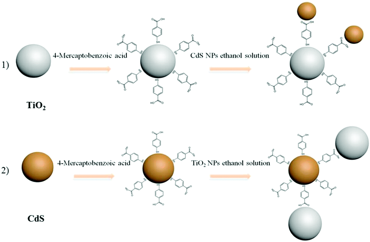 | ||
| Fig. 1 Schematic diagram of the preparation process of the two systems. (1) TiO2/MBA/CdS and (2) CdS/MBA/TiO2. | ||
Instrumentation
The crystal structures of the TiO2 and CdS samples were determined by X-ray diffraction (XRD) using a Siemens D5005 X-ray powder diffractometer with a Cu Kα radiation source at 40 kV and 30 mA. The surface morphologies of the samples were examined using a JEM-2100 transmission electron microscope (TEM) operating at an accelerating voltage of 200 kV. UV-Vis diffuse reflectance spectra (UV-Vis DRS) were recorded on a Hitachi UV-4100 UV-Vis spectrophotometer. Raman spectra were obtained by using a Horiba-Jobin Yvon LabRAM ARAMIS system with a resolution of ca. 4 cm−1. Radiation wavelengths of 633 and 785 nm from an air-cooled HeNe narrow bandwidth laser were used as the excitation source. Data acquisition was the result of the signal 60 s accumulations for the MBA molecules in different assemblies at ambient temperature.Results and discussion
Measurement of TEM and UV-Vis DRS spectra
Fig. 2 shows typical TEM images of TiO2 NPs, TiO2/MBA, TiO2/MBA/CdS, CdS NPs, CdS/MBA, and CdS/MBA/TiO2. Fig. 2a shows that the diameter of the TiO2 NPs is 8 ± 0.51 nm, and the crystal type is an anatase phase (as shown in Fig. S1, ESI†), which is consistent with the literature;32 the observed lattice spacing of 0.351 nm in Fig. 2a corresponds to the (101) plane of anatase (JPCDS 21-1272). After the adsorption of the 4-MBA molecules, no remarkable change is observed. It can be seen from Fig. 2d that the size of the CdS NPs is 5 ± 0.38 nm, and that the lattice spacing of 0.328 nm matches the (111) spacing of the cubic lattice (as shown in Fig. S2, ESI†).36 The sandwich structures, which are assembled between two semiconductors, exhibit strong interactions between the 4-MBA molecules and semiconductor nanoparticles. The 4-MBA molecules are combined with the TiO2 nanoparticles by the thiol group in the TiO2/MBA system.32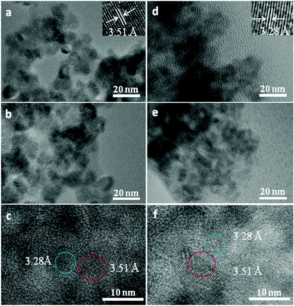 | ||
| Fig. 2 TEM images of (a) TiO2 NPs, (b) TiO2/MBA, (c) TiO2/MBA/CdS, (d) CdS NPs, (e) CdS/MBA, and (f) CdS/MBA/TiO2. | ||
Therefore, in the TiO2/MBA/CdS sandwich system, connective 4-MBA molecules should combine with TiO2 NPs through the thiol group of the molecules due to the formation of Ti–S bonds, which can result in the blue shift of the photoabsorption threshold from the TiO2 band–band transition (as shown in Fig. 3) when connected to the CdS NPs by carboxyl groups. However, the case is the opposite for the CdS/MBA/TiO2 system (i.e., connective 4-MBA molecules combine with CdS NPs through the thiol group of the molecules due to the formation of Cd–S chemical bonds when connected to the TiO2 NPs by carboxyl groups).37
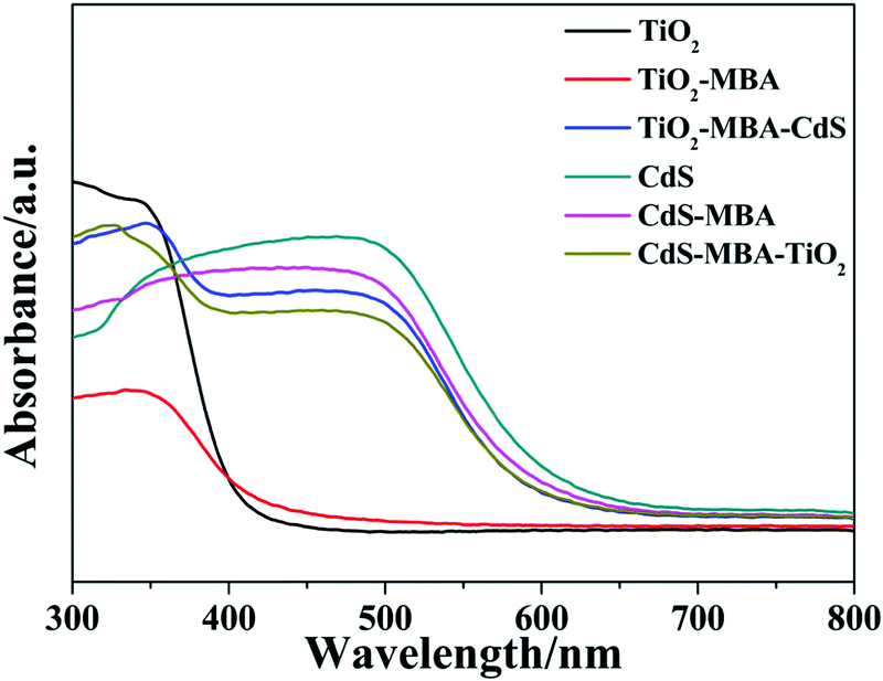 | ||
| Fig. 3 UV-Vis DRS spectra of the TiO2 NPs, CdS NPs and different assemblies. | ||
Fig. 3 shows the UV-Vis DRS spectra of the TiO2 NPs, CdS NPs and different assemblies. The samples (TiO2, TiO2–MBA and TiO2–MBA–CdS) exhibit a wide optical absorption below 400 nm, which is due to the band–band electron transition of TiO2 NPs in accordance with their band gap at ca. 3.2 eV. A long tail from 400–500 nm matches the optical absorption related to the surface state of TiO2 NPs. When TiO2/MBA is compared with pure TiO2 NPs, the optical absorption threshold of the TiO2 band–band transition of the TiO2/MBA sample shows a slight blue shift, and the photoabsorption (approximately 400–500 nm), which is consistent with the surface state of TiO2, is also enhanced. In addition, its optical response is extended to approximately 570 nm. These changes can be ascribed to the interaction between the adsorbed molecules and the TiO2 substrate because of the formation of a charge-transfer complex by the Ti–S bond.32 Similar changes in photoabsorption have been previously reported by Rajh et al.38 in the charge-transfer complexes of enediol molecules with TiO2 NPs. After introducing CdS, the system shows an obvious absorption in the region of 390–490 nm because of the existence of CdS. Moreover, we can also see the wide optical absorption of pure CdS in the region of 390–490 nm. The changes in the absorption peaks in the UV-Vis DRS and X-ray photoelectron spectra (XPS) of the charge-transfer systems (as shown in Fig. S3, ESI†) show that the TiO2–MBA–CdS coupled semiconductor system had been fabricated.
From Fig. 3, the band edge absorption of pure CdS is approximately 510 nm (2.4 eV), which is close to the reported value.39 After modification of the MBA molecules, the photoabsorption threshold of CdS shows a slight blue shift, which can be attributed to the influence of the molecules adsorbed on CdS NPs. After introducing TiO2, the photoabsorption threshold continues to blue shift, and the peak at 290 nm is similar to that of pure TiO2. Therefore, we can draw a conclusion from the changes of the absorption peaks of the UV-Vis DRS and the XPS spectra of the charge-transfer systems (as shown in Fig. S4, ESI†) that the CdS–MBA–TiO2 system is formed.
SERS spectra of 4-MBA in charge-transfer assemblies
To avoid error from the laser power in this experiment (excited at 633 and 785 nm), we normalized all the SERS spectra using the intensity ratio of each peak to the highest peak (1592 cm−1).The SERS spectra measurements of the TiO2/MBA and TiO2/MBA/CdS CdS/MBA and CdS/MBA/TiO2 systems with excitation at 633 nm are shown in Fig. 4a. In addition, the Raman shift and the assignment of the bands are listed in Table 1. For the TiO2/MBA assembly, two strong peaks at approximately 1592 and 1075 cm−1 are assigned to the aromatic totally symmetric stretching mode ν(CC) and the in-plane ring breathing mode coupled with ν(C–S). However, the peak assigned to the in-plane ring breathing mode shifted to 1080 cm−1 in the CdS/MBA assembly. Other weak bands are also observed at approximately 1147 (ν15, b2) and 1182 cm−1 (ν9, a1) in the TiO2/MBA assembly, which are attributed to the C–H deformation modes. In the CdS/MBA assembly, however, we identify a band at 1142 cm−1 (ν15, b2), which is attributed to the C–H deformation modes. Meanwhile, there is a relatively strong peak at 1411 cm−1 due to the COO− symmetric stretching mode in the TiO2/MBA assembly, which can be observed at 1406 cm−1 in the CdS/MBA assembly.
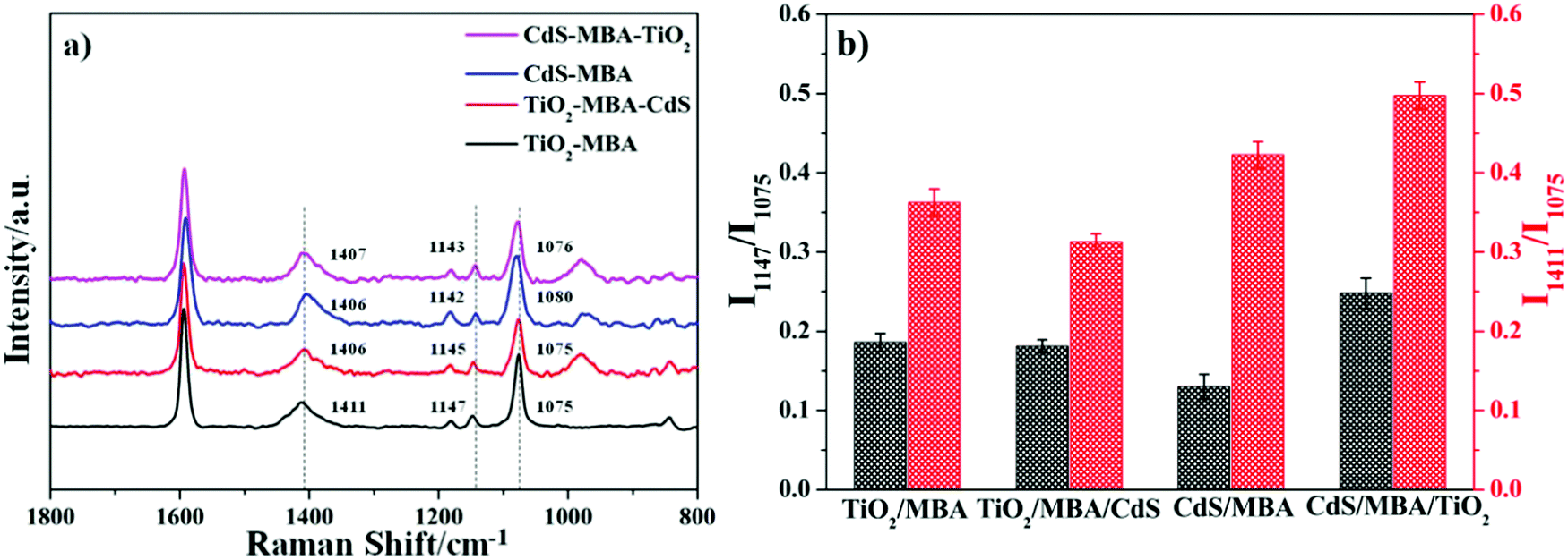 | ||
| Fig. 4 (a) SERS spectra of the TiO2/MBA, TiO2/MBA/CdS, CdS/MBA and CdS/MBA/TiO2 systems at 633 nm excitation; (b) the SERS intensity ratio of the peaks at 1147 and 1075 cm−1 as well as 1411 and 1075 cm−1 in the four systems. | ||
| Wavenumbers (cm−1) | Band assignments | |
|---|---|---|
| On TiO2 | On CdS | |
| a ν, stretching; for ring vibrations, the corresponding vibrational modes of benzene and the symmetry species under C2v symmetry are indicated. | ||
| 1075 | 1080 | In-plane ring breathing + ν(C–S) a1 |
| 1147 | 1142 | C–H deformation modes ν15, b2 |
| 1182 | 1182 | C–H deformation modes ν9, a1 |
| 1411 | 1406 | b(O–H) + ν(C-ph) + 19a + ν(CO2), b2 |
| 1592 | 1592 | Totally symmetric ν(CC), a1 |
After introducing CdS into the TiO2–MBA assembly (from Fig. 4a red line), the Raman band at 1411 cm−1, the characteristic vibration of 4-MBA, visibly shifts to approximately 1406 cm−1, and the peak at 1147 cm−1 (ν15, b2) slightly shifts to approximately 1145 cm−1. Meanwhile, the Raman band at 1080 cm−1 (C–S, a1) obviously moves to 1076 cm−1, and the bands at 1142 cm−1 (ν15, b2) and 1406 cm−1 (ascribed to the COO− symmetric stretching mode) move to 1143 cm−1 and 1047 cm−1 after the introduction of TiO2 into the CdS/MBA assembly, respectively. These peak shifts can be attributed to the interaction between TiO2 and CdS. Interestingly, the peak intensity at 1147 cm−1 (ν15, b2) is not distinctly changed after introducing CdS into the TiO2/MBA assembly. However, the peak at 1142 cm−1 (ν15, b2) in the CdS/MBA assembly became obviously enhanced after the introduction of TiO2.15
According to the charge-transfer model of Lombardi,13 only the totally symmetric vibrational modes of probe molecules are expected to be enhanced via the Franck–Condon contribution, and the Herzberg–Teller effect can enhance both totally and non-totally symmetric vibrational signatures in the SERS spectra. That is, non-totally symmetric vibrational signatures can only be enhanced by the CT mechanism through the Herzberg–Teller contribution. The intensity ratios of the peaks at the b2 mode and the a1 mode can directly identify the charge-transfer progress between the molecules and semiconductor nanoparticles.40,41 In this work, we choose two peaks at 1147 cm−1 (the b2 mode) and 1075 cm−1 (the a1 mode) as the reference peaks for comparison, and we plot the intensity ratio of these two peaks in Fig. 4b. From Fig. 4b (black line), it is clear that the ratio of the b2 and a1 modes in TiO2/MBA/CdS slightly decreases compared to that of the TiO2/MBA assembly. Nevertheless, the intensity ratios of the peaks at 1147 cm−1 and 1075 cm−1 in CdS/MBA/TiO2 obviously increase compared to the CdS/MBA assembly. Furthermore, the non-totally symmetric vibrational signatures in the CdS/MBA/TiO2 assembly, which can be efficiently enhanced by the charge-transfer process, are obviously stronger than those of the TiO2/MBA/CdS assembly.
To confirm the phenomenon, we also plot the intensity ratio of the two peaks at 1411 cm−1 (the b2 mode) and 1075 cm−1 (the a1 mode), as shown in Fig. 4b (red line), and the same conclusion is obtained. These results demonstrate that the assembly sequence method largely influences the charge-transfer degree, which means that the assembly direction of the MBA molecules directly controls the charge-transfer process. The same phenomenon can be seen in the Raman spectra under excitation at 785 nm; the Raman spectra and the intensity ratio of the peaks at 1147 cm−1 and 1075 cm−1, and 1411 cm−1 and 1075 cm−1 are shown in Fig. S5 (ESI†). It can be seen that the COO− group shows excitation wavelength dependence in the four systems as shown in Fig. 4b and Fig. S5b (ESI†), which is more obvious in the CdS–MBA system.
Notably, the ratio of I1411 and I1075 in CdS–MBA is greatly larger compared to I1147 and I1075. The COO− group, which gives a band at 1411 cm−1, possesses a strong electron attraction capability. When the molecules get absorbed on the CdS, the strong electronegativity of COO− caused an increase in the electron cloud around the carboxyl group, which is obviously larger than that of the C–H (peak at 1147 cm−1). The apparent charge-transfer degree of the COO− group is larger than that in the C–H group, which causes a larger ratio of I1411 and I1075 in the CdS–MBA than the ratio of I1147 and I1075. At the same time, the electronegativity of TiO2 is dramatically larger than that of CdS. In the CdS–MBA assembly, the electron cloud around the carboxyl group is much stronger than that in the TiO2–MBA and TiO2–MBA–CdS assemblies. The ratio of I1411 and I1075 in CdS–MBA is much larger than those in TiO2–MBA and TiO2–MBA–CdS, which provides the importance of the assembly direction of the MBA molecules between the two kinds of semiconductors.
CT mechanism of MBA in semiconductor–semiconductor systems
In this experiment, we formed semiconductor–molecule–semiconductor sandwich structures with two kinds of semiconductor nanoparticles; they are CdS, with the valence band (VB) at 6.23 eV and the conduction band (CB) at 3.98 eV, and TiO2 with the VB at 7.4 eV and the CB at 4.2 eV as shown in Scheme 1.2 The molecule connecting these two semiconductor nanoparticles is MBA, with its highest occupied molecular orbital (HOMO) at 8.48 eV and its lowest unoccupied molecular orbital (LUMO) at 3.85 eV.42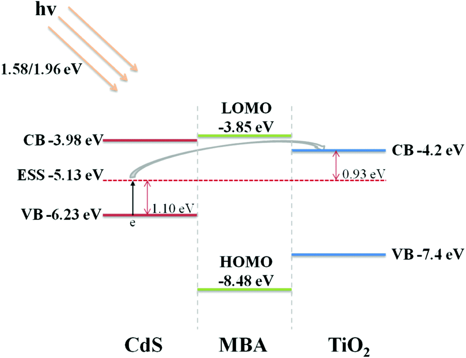 | ||
| Scheme 1 Energy levels of TiO2, 4-MBA and CdS. | ||
To further confirm the charge-transfer process in these sandwich structures, the work functions of the semiconductors were compared. According to the previous literature, the work function of CdS is 4.5 eV, which is lower than that of TiO2, whose work function is 4.7 eV,43,44 meaning that, when these two semiconductors form a charge conduction system, the electrons must flow from the smaller work function material to the larger work function material, and in these two systems, the flow occurs in the direction from CdS to TiO2.
Additionally, the surface-state energy level (ESS) of CdS is 5.13 eV,45 which is 1.1 eV higher than the VB level of CdS and 0.93 eV lower than the CB level of TiO2. The ESS level of CdS forms a bridge from the VB of CdS to the CB of TiO2. In our experiment, the laser wavelengths used here are 633 nm and 785 nm, and the corresponding energies of the photons are 1.96 eV and 1.58 eV, respectively. Obviously, the energy of the laser photons is larger than the band gap from the VB of CdS to the ESS of CdS, or the ESS of CdS to the CB of TiO2. When these sandwich structures are excited by the laser, electrons in the VB of CdS could be excited into the ESS of CdS, and then, jump to a higher level, e.g., the CB of TiO2. In these assemblies, meanwhile, the MBA molecules function as a bridge between the semiconductors and play an important role as a transmitter. From the intensity ratio of the peaks attributed to the b2 mode and peaks attributed to the a1 mode of these two sandwich assemblies, the assembly direction of MBA between these two semiconductors deeply influences the charge-transfer process. That is, the thiol group of MBA tends to preferentially connect with the surface of the semiconductors. When the order of the assembly process is TiO2–MBA–CdS, the thiol group of MBA attached to the TiO2 nanoparticles, while the carboxyl group of MBA attached to the CdS nanoparticles. The strong electronegativity of the carboxyl group in the MBA molecule forms a negative center, when electrons transfer from CdS to TiO2, and the negative center of MBA hinders the transmission process of the electrons and causes a weaker selective enhancement of the b2 mode. In contrast, when the assembly order is CdS–MBA–TiO2, the thiol group of MBA attached to the CdS nanoparticles, and meanwhile, the thiol group of the MBA molecule forms a positive center and promotes the electron transfer from CdS to TiO2 due to a stronger selective enhancement of the b2 mode.
Conclusion
In this work, two systems (TiO2/MBA/CdS and CdS/MBA/TiO2) have been fabricated to explore the charge-transfer process at the interface between TiO2 and CdS nanoparticles by the SERS technique. According to the energy levels and work function of TiO2 and CdS, the charge-transfer direction of the TiO2–MBA–CdS and CdS–MBA–TiO2 systems is from CdS to TiO2 under laser excitation wavelengths at 633 and 785 nm. The inner polarity of the molecule (4-MBA here) can dramatically influence the charge-transfer process when it is assembled at the interface between two kinds of semiconductors. By changing the assembly direction of the 4-MBA molecules, we formed two different kinds of sandwich assemblies. According to the analysis of the SERS spectra of these systems under excitation wavelengths at 633 and 785 nm, the peak assigned to the b2 mode was significantly enhanced in the CdS–MBA–TiO2 system, but in the TiO2–MBA–CdS system, it was barely enhanced because the dipole direction of the MBA molecules hindered the charge-transfer process from CdS to TiO2, and the charge-transfer process was slightly weaker in TiO2–MBA–CdS assemblies. These results provide details about the charge-transfer process at the interface of the semiconductor nanoparticles, and also prove that the SERS technique has surprising application prospects in the field of nanomaterials.Conflicts of interest
The authors declare no competing financial interest.Acknowledgements
The research was supported by the National Natural Science Foundation (Grants 21773080, 21711540292, and 21773079) of the People's Republic of China.References
- I. Robel, V. Subramanian, M. Kuno and P. V. Kamat, Quantum dot solar cells. Harvesting light energy with CdSe nanocrystals molecularly linked to mesoscopic TiO2 films, J. Am. Chem. Soc., 2006, 128, 2385–2393 CrossRef CAS PubMed.
- H. Lee, H. C. Leventis, S. J. Moon, P. Chen, S. Ito, S. A. Haque, T. Torres, F. Nüesch, T. Geiger, S. M. Zakeeruddin, M. Grätzel and M. K. Nazeeruddin, PbS and CdS quantum dot-sensitized solid-state solar cells: “Old concepts, new results”, Adv. Funct. Mater., 2009, 19, 2735–2742 CrossRef CAS.
- R. W. Crisp, D. M. Kroupa, A. R. Marshall, E. M. Miller, J. Zhang, M. C. Beard and J. M. Luther, Metal halide solid-state surface treatment for high efficiency PbS and PbSe QD solar cells, Sci. Rep., 2015, 5, 9945 CrossRef CAS PubMed.
- M. A. Zhukovskiy, A. L. Stroyuk, V. V. Shvalagin, N. P. Smirnova, O. S. Lytvyn and A. M. Eremenko, Photocatalytic growth of CdS, PbS, and CuxS nanoparticles on the nanocrystalline TiO2 films, J. Photochem. Photobiol., A, 2009, 203, 137–144 CrossRef CAS.
- S. Qian, C. Wang, W. Liu, Y. Zhu, W. Yao and X. Lu, An enhanced CdS/TiO2 photocatalyst with high stability and activity: effect of mesoporous substrate and bifunctional linking molecule, J. Mater. Chem., 2011, 21, 4945 RSC.
- R. S. Dibbell, G. R. Soja, R. M. Hoth and D. F. Watson, Photocatalytic patterning of monolayers for the site-selective deposition of quantum dots onto TiO2 surfaces, Langmuir, 2007, 23, 3432–3439 CrossRef CAS PubMed.
- B. R. Hyun, Y. W. Zhong, A. C. Bartnik, L. Sun, H. D. Abruna, F. W. Wise, J. D. Goodreau, J. R. Matthews, T. M. Leslie and N. F. Borrelli, Electron injection from colloidal PbS quantum dots into titanium dioxide nanoparticles, ACS Nano, 2008, 2, 2206–2212 CrossRef CAS PubMed.
- Y. Bessekhouad, D. Robert and J. V. Weber, Bi2S3/TiO2 and CdS/TiO2 heterojunctions as an available configuration for photocatalytic degradation of organic pollutant, J. Photochem. Photobiol., A, 2004, 163, 569–580 CrossRef CAS.
- K. E. Lee, M. A. Gomez, T. Regier, Y. Hu and G. P. Demopoulos, Further understanding of the electronic interactions between N719 sensitizer and anatase TiO2 films: a combined X-ray absorption and X-ray photoelectron spectroscopic study, J. Phys. Chem. C, 2011, 115, 5692–5707 CrossRef CAS.
- W. E. Doering and S. Nie, Single-molecule and single-nanoparticle SERS: examining the roles of surface active sites and chemical enhancement, J. Phys. Chem. B, 2002, 106, 311–317 CrossRef CAS.
- A. Otto, The ‘chemical’ (electronic) contribution to surface-enhanced Raman scattering, J. Raman Spectrosc., 2005, 36, 497–509 CrossRef CAS.
- J. R. Lombardi and R. L. Birke, A Unified View of Surface-Enhanced Raman Scattering, Acc. Chem. Res., 2009, 42, 734–742 CrossRef CAS PubMed.
- J. R. Lombardi and R. L. Birke, A Unified Approach to Surface-Enhanced Raman Spectroscopy, J. Phys. Chem. C, 2008, 112, 5605–5617 CrossRef CAS.
- L. Yang, X. Jiang, W. Ruan, J. Yang, B. Zhao, W. Xu and J. R. Lombardi, Charge-transfer-induced surface-enhanced Raman scattering on Ag−TiO2 nanocomposites, J. Phys. Chem. C, 2009, 113, 16226–16231 CrossRef CAS.
- X. Jiang, X. Li, X. Jia, G. Li, X. Wang, G. Wang, Z. Li, L. Yang and B. Zhao, Surface-enhanced Raman scattering from synergistic contribution of metal and semiconductor in TiO2/MBA/Ag(Au) and Ag(Au)/MBA/TiO2 assemblies, J. Phys. Chem. C, 2012, 116, 14650–14655 CrossRef CAS.
- Z. Mao, W. Song, X. Xue, W. Ji, Z. Li, L. Chen, H. Mao, H. Lv, X. Wang, J. R. Lombardi and B. Zhao, Interfacial charge-transfer effects in semiconductor–molecule–metal structures: influence of contact variation, J. Phys. Chem. C, 2012, 116, 14701–14710 CrossRef CAS.
- X. Wang, Y. Wang, H. Sui, X. Zhang, H. Su, W. Cheng, X. X. Han and B. Zhao, Investigation of charge transfer in Ag/N719/TiO2 interface by surface-enhanced Raman spectroscopy, J. Phys. Chem. C, 2016, 120, 13078–13086 CrossRef CAS.
- X. Wang, B. Zhao, P. Li, X. X. Han and Y. Ozaki, Charge transfer at the TiO2/N3/Ag interface monitored by surface-enhanced Raman spectroscopy, J. Phys. Chem. C, 2017, 121, 5145–5153 CrossRef CAS.
- E. Hutter and J. H. Fendler, Exploitation of localized surface plasmon resonance, Adv. Mater., 2004, 16, 1685–1706 CrossRef CAS.
- R. Himstedt, P. Rusch, D. Hinrichs, T. Kodanek, J. Lauth, S. Kinge, L. D. A. Siebbeles and D. Dorfs, Localized surface plasmon resonances of various nickel sulfide nanostructures and Au–Ni3S2 core–shell nanoparticles, Chem. Mater., 2017, 29, 7371–7377 CrossRef CAS.
- T.-L. Li, Y.-L. Lee and H. Teng, High-performance quantum dot-sensitized solar cells based on sensitization with CuInS2 quantum dots/CdS heterostructure, Energy Environ. Sci., 2012, 5, 5315–5324 RSC.
- Z. Yang, C. Y. Chen, C. W. Liu and H. T. Chang, Electrocatalytic sulfur electrodes for CdS/CdSe quantum dot-sensitized solar cells, Chem. Commun., 2010, 46, 5485–5487 RSC.
- Z. Yang, C.-Y. Chen, C.-W. Liu, C.-L. Li and H.-T. Chang, Quantum dot-sensitized solar cells featuring CuS/CoS electrodes provide 4.1% efficiency, Adv. Energy Mater., 2011, 1, 259–264 CrossRef CAS.
- G. Zhu, T. Xu, T. Lv, L. Pan, Q. Zhao and Z. Sun, Graphene-incorporated nanocrystalline TiO2 films for CdS quantum dot-sensitized solar cells, J. Electroanal. Chem., 2011, 650, 248–251 CrossRef CAS.
- M. L. Brongersma, N. J. Halas and P. Nordlander, Plasmon-induced hot carrier science and technology, Nat. Nanotechnol., 2015, 10, 25–34 CrossRef CAS PubMed.
- N. Serpone, P. Pichat, J. M. Herrmann, E. PelizzettiM, L. Brongersma, N. J. Halas and P. Nordlander, Inter-particle electron transfer in semiconductor dispersions: a new strategy in photocatalysis, J. Am. Chem. Soc., 1987, 109, 6632 CrossRef.
- L. Spanhel, H. Weller, A. Fojtik and A. Henglein, Photochemistry of semiconductor colloids. Part 17. Strong luminescing CdS and CdS-Ag2S particles, ChemInform, 1987, 18, 88–94 Search PubMed.
- K. R. Gopidas, M. Bohorquez and P. V. Kamat, Photoelectrochemistry in semiconductor particulate systems. Part 16. Photophysical and photochemical aspects of coupled semiconductor, ChemInform, 1990, 21, 9045 CrossRef.
- R. G. Chaudhuri and S. PariaJ, Optical properties of double-shell hollow ZnS-Ag2S nanoparticles, J. Phys. Chem. C, 2013, 117, 23385–23390 CrossRef.
- Y. Wang, Z. Sun, Y. Wang, H. Hu, B. Zhao, W. Xu and J. R. Lombardi, Surface-Enhanced Raman Scattering on mercaptopyridine-capped CdS microclusters, Spectrochim. Acta, Part A, 2007, 66, 1199–1203 CrossRef PubMed.
- X. Xue, W. Ji, Z. Mao, Z. Li, W. Ruan, B. Zhao and J. R. Lombardi, Effects of Mn doping on surface enhanced Raman scattering properties of TiO2 nanoparticles, Spectrochim. Acta, Part A, 2012, 95, 213–217 CrossRef CAS PubMed.
- L. Yang, X. Jiang, W. Ruan, B. Zhao, W. Xu and J. R. Lombardi, Observation of enhanced Raman scattering for molecules adsorbed on TiO2 nanoparticles: charge-transfer contribution, J. Phys. Chem. C, 2008, 112, 20095–20098 CrossRef CAS.
- X. Xue, W. Ji, Z. Mao, H. Mao, Y. Wang, X. Wang, W. Ruan, B. Zhao and J. R. Lombardi, Raman investigation of nanosized TiO2: effect of crystallite size and quantum confinement, J. Phys. Chem. C, 2012, 116, 8792–8797 CrossRef CAS.
- L. Yang, X. Jiang, W. Ruan, B. Zhao, W. Xu and J. R. Lombardi, Adsorption study of 4-MBA on TiO2 nanoparticles by surface-enhanced Raman spectroscopy, J. Raman Spectrosc., 2009, 40, 2004–2008 CrossRef CAS.
- W. Baiqi, J. Liqiang, Q. Yichun, L. Shudan, J. Baojiang, Y. Libin, X. Baifu and F. Honggang, Enhancement of the photocatalytic activity of TiO2 nanoparticles by surface-capping DBS groups, Appl. Surf. Sci., 2006, 252, 2817–2825 CrossRef.
- P. C. Dey and R. Das, Photoluminescence quenching in ligand free CdS nanocrystals due to silver doping along with two high energy surface states emission, J. Lumin., 2017, 183, 368–376 CrossRef CAS.
- R. S. Das and Y. K. Agrawal, Raman spectroscopy: recent advancements, techniques and applications, Vib. Spectrosc., 2011, 57, 163–176 CrossRef CAS.
- T. Rajh, L. X. Chen, K. Lukas, T. Liu, M. C. Thurnauer and D. M. Tiede, Surface restructuring of nanoparticles: an efficient route for ligand–metal oxide crosstalk, J. Phys. Chem. B, 2002, 106, 10543–10552 CrossRef CAS.
- W. E. Mahmoud, Synthesis and characterization of 2A-3SHPA decorated ZnS@CdS core–shell heterostructure nanowires as a fluorescence probe for antimony ions detection, Sens. Actuators, B, 2017, 238, 1001–1007 CrossRef CAS.
- X. Zhang, H. Sui, X. Wang, H. Su, W. Cheng, X. Wang and B. Zhao, Charge transfer process at the Ag/MPH/TiO2 interface by SERS: alignment of the Fermi level, Phys. Chem. Chem. Phys., 2016, 18, 30053–30060 RSC.
- R. Han, W. Song, X. Wang, Z. Mao, X. X. Han and B. Zhao, Investigation of charge transfer at the TiO2-MBA-Au interface based on surface-enhanced Raman scattering: SPR contribution, Phys. Chem. Chem. Phys., 2018, 20, 5666–5673 RSC.
- X. Xue, W. Ji, Z. Mao, C. Zhao, B. Zhao and J. R. Lombardi, Simultaneous enhancement of phonons modes with molecular vibrations due to Mg doping of a TiO2 substrate, RSC Adv., 2013, 3, 20891 RSC.
- K. P. Bhandari, P. J. Roland, H. Mahabaduge, N. O. Haugen, C. R. Grice, S. Jeong, T. Dykstra, J. Gao and R. J. Ellingson, Thin film solar cells based on the heterojunction of colloidal PbS quantum dots with CdS, Sol. Energy Mater. Sol. Cells, 2013, 117, 476–482 CrossRef CAS.
- A. R. Kumarasinghe, W. R. Flavell, A. G. Thomas, A. K. Mallick, D. Tsoutsou, C. Chatwin, S. Rayner, P. Kirkham, S. Warren, S. Patel, P. Christian, P. O'Brien, M. Gratzel and R. Hengerer, Electronic properties of the interface between p-CuI and anatase-phase n-TiO2 single crystal and nanoparticulate surfaces: a photoemission study, J. Chem. Phys., 2007, 127, 114703 CrossRef CAS PubMed.
- J. L. a. H. C. G. C. L. Balestra, Determination of surface state energy positions by surface photovoltage spectrometry: CdS, Surf. Sci., 1971, 26, 317–320 CrossRef.
Footnote |
| † Electronic supplementary information (ESI) available. See DOI: 10.1039/c8nj04003f |
| This journal is © The Royal Society of Chemistry and the Centre National de la Recherche Scientifique 2019 |