
High-adhesion vertically aligned gold nanowire stretchable electrodes via a thin-layer soft nailing strategy†
Yunzhi
Ling
ab,
Keying
Guo
bc,
Bowen
Zhu
ab,
Beatriz
Prieto-Simon
bc,
Nicolas H.
Voelcker
 bc and
Wenlong
Cheng
*ab
bc and
Wenlong
Cheng
*ab
aDepartment of Chemical Engineering, Monash University Clayton, Victoria 3800, Australia. E-mail: wenlong.cheng@monash.edu
bMelbourne Centre for Nanofabrication, Victorian Node of the Australian National Fabrication Facility, Clayton, Victoria 3168, Australia
cDrug Delivery, Disposition and Dynamics, Monash Institute of Pharmaceutical Sciences, Monash University, Parkville, Victoria 3052, Australia
First published on 29th May 2019
Abstract
A stretchable electrode is a crucial component in future elastronics (i.e. stretchable electronics) with implications in soft actuators, healthcare monitoring, and robotics to name a few. The performance of the stretchable electrode is generally evaluated in terms of three key aspects: sensitivity, stretchability, and durability. While encouraging progress has been made in the first two aspects, long-term stability remains a challenge because of failure at the soft/hard materials interface between active materials and elastomeric substrates. Here, we propose a new microsphere lithography-based strategy to pattern vertically aligned gold nanowires (v-AuNWs) with quasi-ordered pinholes, allowing ‘nailing’ of PDMS into the pinholes. This enabled substantially enhanced interfacial adhesion of 24 times greater than that without microsphere lithography. Moreover, the pinhole size in the v-AuNW film could be tuned from an average diameter of 0.4 to 2.8 μm. Both experimental and simulation results demonstrate that the sensitivity increased as the pinhole size increased. Our strategy represents a novel route to fabricate robust elastronic electrodes for potential applications in next-generation wearable and implantable devices.
New conceptsDurability is one of the critical factors to estimate the performance of stretchable electrodes. However, the durability still remains a challenge because the huge Young's modulus difference between inorganic filler materials and elastomeric substrates always leads to delamination under repeated mechanical deformation. Here we report a robust high-adhesion stretchable electrode by embedding vertically aligned standing gold nanowires (v-AuNWs) into PDMS through a microsphere lithography technique. Through controlling the Au seed distribution, we successfully synthesized a v-AuNW film consisting of quasi-hexagonal lattice pinholes. Inspired by the construction material nails, which are commonly used for connecting two separated parts by hammering them together, we cast liquid PDMS into pinholes in a v-AuNW film, serving as PDMS nails to achieve a high-adhesion v-AuNW stretchable electrode. Compared with the counterpart without PDMS nails, the v-AuNWs with PDMS nails increase 17.3 fold in adhesive strength. Besides, the obtained PDMS nails also redistribute strain energy by focusing stress in-between the PDMS nails, with a 3.1 fold increase in the strain sensitivity of the v-AuNW stretchable electrode. The novel metal/polymer interface design may offer an effective strategy for robust stretchable electrodes with high adhesion for future elastronics. |
Introduction
Stretchable electrodes have been considered as an extremely important component in the next-generation stretchable electronics, namely elastronics,1 which can have numerous applications including soft robotics,2,3 wearable electronics,4 implantable bioelectronics5,6 and internet of things.7,8 These stretchable electrodes or sensors are classified into resistive,9–12 capacitance,13,14 piezoelectric and triboelectric,15–18 based on their signal transduction mechanisms. Generally speaking, a stretchable electrode is composed of active conductive materials (e.g., carbon and metals) and an elastic substrate (e.g., polydimethylsiloxane (PDMS), Ecoflex and polyurethane).12 One critical challenge is the weak adhesion between inorganic conductive materials and the organic substrate, due to the mismatch in mechanical properties by orders of magnitude differences in Young's moduli.19 Hence, conductive materials are prone to delaminate from the elastic substrate under repeating mechanical loads, and the situation is especially serious when the stretchable electrode is designed for long-term on-body or in-body uses where device durability is a must.Until now, several methods have been proposed to realize better adhesion between active materials and an elastic substrate. Two strategies in particular are usually considered: one is based on construction of an embedding structure, and another one is to introduce an adhesive layer on the elastomer surface.20,21 The former one is to embed part of the conductive materials into the substrate, like the root structure of a tree, which stands firmly by stretching its roots into the soil. For example, a high-adhesion gold stretchable electrode was obtained by embedding a fraction of gold into a PDMS substrate, which led to 10.4 fold enhancement in adhesive strength compared with a non-embedded counterpart.22 The latter strategy focuses on surface modification of a substrate in order to produce bonding. A binder of poly(dopamine) coated on PDMS is commonly used to induce intimate contact between silver nanowires and PDMS, enhancing both the adhesion and durability of the resulting stretchable electrode.23 Besides, 3-aminopropyltrimethoxysilane (APTMS) is an excellent molecular glue for gold. A layer of APTMS molecules containing organosilanes and amine groups is designed to interact strongly both with the hydroxyl-modified substrate and the gold surfaces, thereby promoting surface adhesion.24,25
Here, we report on a new strategy for enhancing interfacial bonding by patterning vertically aligned gold nanowires (v-AuNWs) with quasi-ordered pinholes, followed by ‘nailing’ with PDMS. We have recently discovered Janus material properties and superior stretchability of v-AuNW-bonded elastomers, demonstrating applications in pressure, strain and biological sensing.25–27 In comparison to the printing nanowires which usually form percolation networks on an elastomeric substrate, v-AuNWs are chemically bonded to elastomers via an amine-Au bonding interaction,25,26 as illustrated in the ESI,† Fig. S1. Besides, our v-AuNW-based strategy may offer the following attributes: high stretchability due to an accordion fan-like deformation process;25 high conductivity due to closely-packed nanowire structures;26 direct solution-based growth allowing for conformal coating to virtually any topological complex surfaces including human hair, fish lines, smooth or rough surfaces or multiple layered structures;26 high surface area in conjunction with high conductivity enabling their application as electrochemical electrodes which are not yet easily achieved with printing nanowires27–29
In this work, we further demonstrate facile interface control for designing well-defined cylinder pinhole interfaces to promote interfacial adhesion. Remarkably, we now show that the v-AuNW growth is compatible with the known microsphere lithography, allowing for patterning of quasi-hexagonal lattice pinholes. Inspired by the construction material nails, which are commonly used for connecting two separated parts by hammering them together, we cast liquid PDMS into the pinholes, serving as PDMS nails to achieve the high-adhesion electrode. Compared with the counterpart without PDMS nails, the v-AuNWs with PDMS nails achieved a ∼17.3 fold increase in the adhesive strength. Moreover, we also found that the obtained PDMS nails played a role in redistributing the strain energy by focusing stress in-between the PDMS nails, leading to ∼3.1 fold increase in strain sensitivity.
Results and discussion
Fig. 1a illustrates the typical fabrication process of the pinhole v-AuNW film. A monolayer of polystyrene (PS) microspheres (with an average diameter of 4.5 μm) was firstly fabricated by means of colloidal convective assembly on a piranha-pretreated silicon wafer. As a thermoplastic polymer, PS begins to flow if the heating temperature is set above its glass transition temperature (95 °C–100 °C).30,31 Under an annealing temperature of 110 °C, the crystallized PS microspheres were partially melted and adhered to the wafer substrate. After silanization with APTMS vapor inside a vacuum desiccator overnight, the wafer with deformed PS microspheres was dipped into Au seed solution to complete the seed deposition through electrostatic self-assembly.26,32,33 Since the Au seeds only assembled in the area where PS microspheres were absent, the Au seed pattern with pinholes were developed after removal of PS microspheres in toluene. Finally, patterned pinhole v-AuNW films were obtained after their immersion into the growth solution containing gold precursor, ligand and reducing agent. Details of the fabrication process are described in the Experimental section.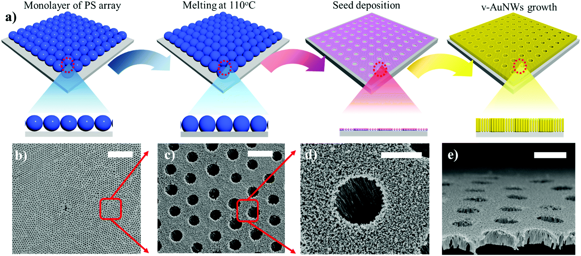 | ||
| Fig. 1 Design of the pinhole v-AuNW stretchable electrode. (a) Schematic illustration of the fabrication of the pinhole v-AuNW film by means of the microsphere lithography technique; (b) SEM images of the pinhole v-AuNW film on a large scale. Scale bar: 50 μm. (c and d) Enlarged views of panel (b), scale bars for c and d are 5 μm and 2 μm, respectively; (e) cross-sectional view of the pinhole v-AuNW film, scale bar: 3 μm. | ||
Fig. 1b shows the SEM images of the pinhole v-AuNW film, with pinholes quasi-hexagonally arranged. From its enlarged views (Fig. 1c and d), we can clearly see that each pinhole is of circular circumference. The cross-sectional view (Fig. 1e) illustrates that v-AuNWs are vertically aligned and each hole is of a cylindrical shape.
It is expected that the size of the melted PS microspheres will determine the pinhole size in the v-AuNW film. To prove this, we further investigated the influence of melting duration on the pinhole size, as shown by the detailed scanning electron microscopy (SEM) characterizations in the ESI,† Fig. S2, with the corresponding measurement summarized in the ESI,† Table S1. From the top views (ESI,† Fig. S3a–g), one can clearly see that all the PS microspheres are closely-packed. Since the heat transferred from the hotplate to the underneath of the PS microsphere arrays, the bottom parts severely melted while the top parts remain intact because of the surrounding ambient cool air. However, fusion occurred when the heating durations exceeded ∼60 s. The cross-sectional views (ESI,† Fig. S3h–n) show the contact area between the melted PS microspheres and silicon wafer increasing gradually with the increasing durations from 0 s to 120 s. Typically, for 0 s heating, the PS substrate contact cross-sectional size was 0.3 ± 0.1 μm, which increased 3.1 ± 0.4 μm for 30 s heating. The resulting pinhole sizes of v-AuNWs film were consistent with the melted area of the PS microspheres, which was verified by SEM images of the pinhole v-AuNW film (ESI,† Fig. S3o–u) and ESI,† Table S1. It should be noted that continuous and percolating v-AuNWs could not be formed when the heating duration exceeded 60 s because excessive heating caused the melting between the neighboring PS microspheres.
In the woodworking and construction industry, nails are the most commonly used material for joining two separate pieces by hammering them together. Inspired by this, we cast liquid PDMS into the pinholes of the v-AuNW film to be “PDMS nails” after being cured. Similar to woodworking nails, these PDMS nails were able to tightly connect the v-AuNWs film and the PDMS substrate so as to achieve a high-adhesion stretchable electrode. The dimensions of the AuNW array before and after PDMS casting were characterized by atomic force microscopy (AFM) (ESI,† Fig. S3). The pinholes can be clearly observed in the ESI,† Fig. S3a, while the surface became smoother after those pinholes were filled with PDMS (ESI,† Fig. S3b).
Remarkably, our thin-layer nailing fabrication strategy was compatible with conventional photolithography, enabling facile patterning structures. To demonstrate this, a patterned photoresist was fabricated on a silicon wafer by a 300 μm microelectrode photomask, as shown in the ESI,† Fig. S4a. Then PS microspheres were assembled onto the patterned structures, which was followed by deposition of gold seeds and polystyrene removal. This enabled site-specific AuNW growth to where gold seeds were deposited. Upon PDMS infiltration, a patterned pinhole stretchable microelectrode could be obtained (ESI,† Fig. S4b). Such patternability may be important for future integration for applications in soft actuators, healthcare monitoring, and robotics, etc.
A Scotch tape test was performed to investigate the adhesion between v-AuNWs and the PDMS (Fig. 2a and d). For v-AuNWs/PDMS without a nail structure, the v-AuNWs were easily peeled off, whereas no peeled v-AuNWs were observed for the pinhole v-AuNWs/PDMS electrode. Fig. 2b and e show the top-view SEM images of v-AuNWs/PDMS electrodes with and without pinhole structures, respectively. The blurring domains in Fig. 2e might come from the charging effects of PDMS “nails”, which had an average diameter of ∼3.1 μm. To visualize further soft/hard interface structures with/without embedding, we utilized focused ion beam (FIB) to mill the v-AuNWs/PDMS stretchable electrode. As shown in Fig. 2c, v-AuNWs were closely-packed rendering it difficult for viscous PDMS to permeate into the interstices. In contrast, liquid PDMS could spread into the micrometer-sized pinholes as shown in Fig. 2f. Therefore, the presence of pinholes essentially led to a “curved interlocking interface”, substantially increasing the soft/hard contact area. This rendered it difficult to debond during mechanical deformation as supported by finite elemental modelling shown in Fig. 2g and Supplemental Video 1, ESI.† When the same pulling force was applied, the stress required for a pinhole structure (Fig. 2g bottom) was much larger than that of a planar interface (Fig. 2g top). This was because the “nail-like” interlocking interface required greater resistance to be overcome for debonding.
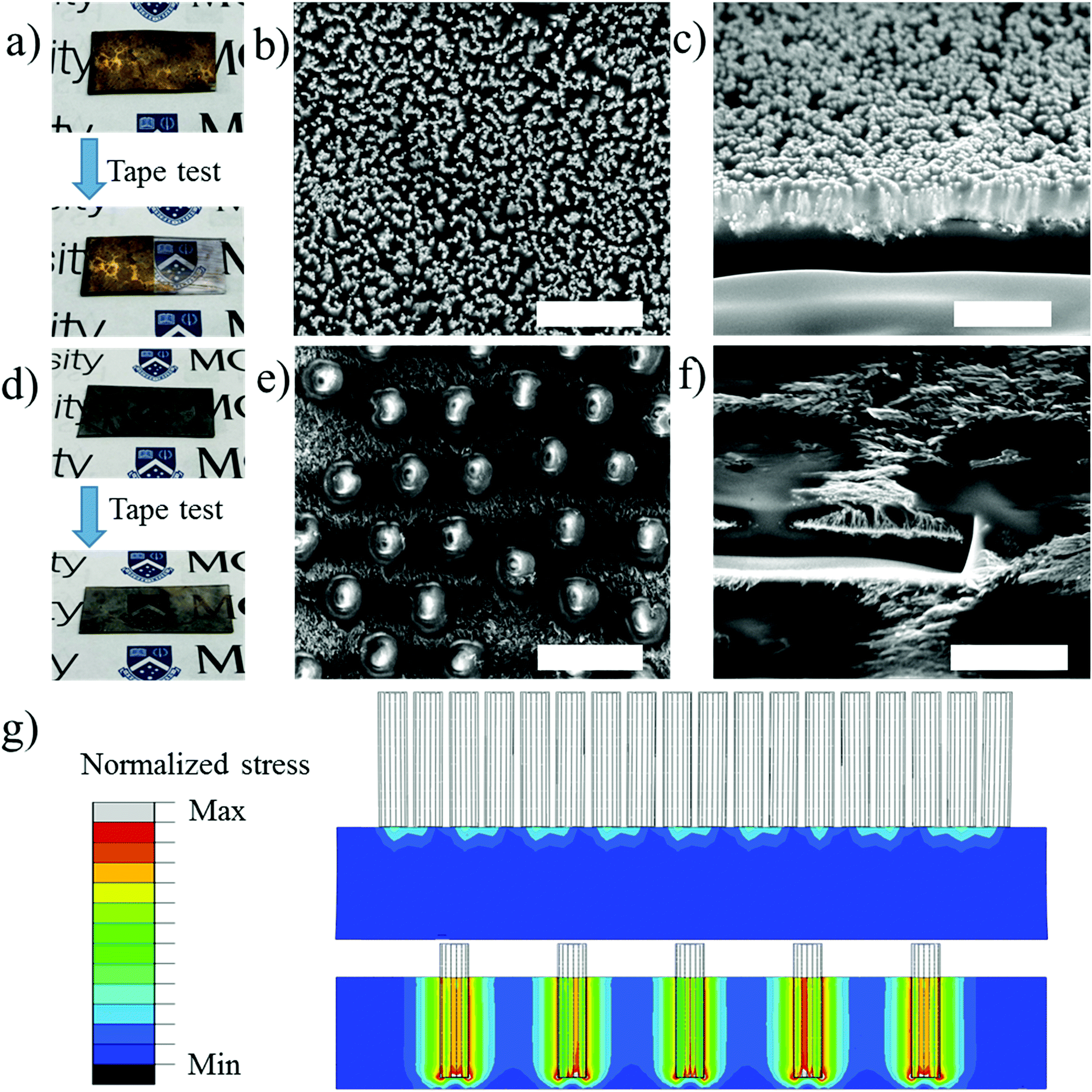 | ||
| Fig. 2 The mechanism of adhesive enhancement for the pinhole v-AuNW stretchable electrode. (a) Tape peeling test of v-AuNWs on PDMS; (b) top-view and (c) cross-section SEM image of v-AuNWs on PDMS, scale bars: 1 μm. (d) Tape peeling test of v-AuNWs with the PDMS nail structure; (e) top-view and (f) cross-section SEM image of v-AuNWs with the PDMS nail structure, scale bars: 1 μm. (g) Finite element analysis of stress distribution of v-AuNWs on PDMS (top) and v-AuNWs with PDMS nails (bottom) when a vertical pulling force is applied. | ||
Furthermore, to quantify the adhesion strength, a commonly-used standard peeling test was performed that involves a rigid stick with epoxy resin glue.22,34 The adhesive strength of the pinhole v-AuNWs/PDMS electrode (the average diameter of pinhole (2R) was 1.1 μm) was measured to be 0.75 ± 0.12 MPa, which is 7.5 fold higher than that of v-AuNWs on PDMS, shown in Fig. 3b. A similar enhancement was observed for other heating times. For 30 s heating (2R was 2.8 μm), the adhesive strength reached a value of 2.64 ± 0.32 MPa. Clearly, larger-sized pinholes led to greater interfacial adhesion. This may be because the larger diameter pinhole had a larger interfacial surface between v-AuNWs and the PDMS substrate, which caused a greater friction force. We also found that the height of v-AuNWs could be tuned by adjusting the incubation time in the growth solution, shown in the ESI,† Fig. S5, e.g. ∼200 nm for 30 s and ∼1200 nm for 180 s. This allowed us to investigate how the height of v-AuNWs influenced the adhesive strength (Fig. 3c). The results indicate that the taller v-AuNWs led to a larger adhesive strength.
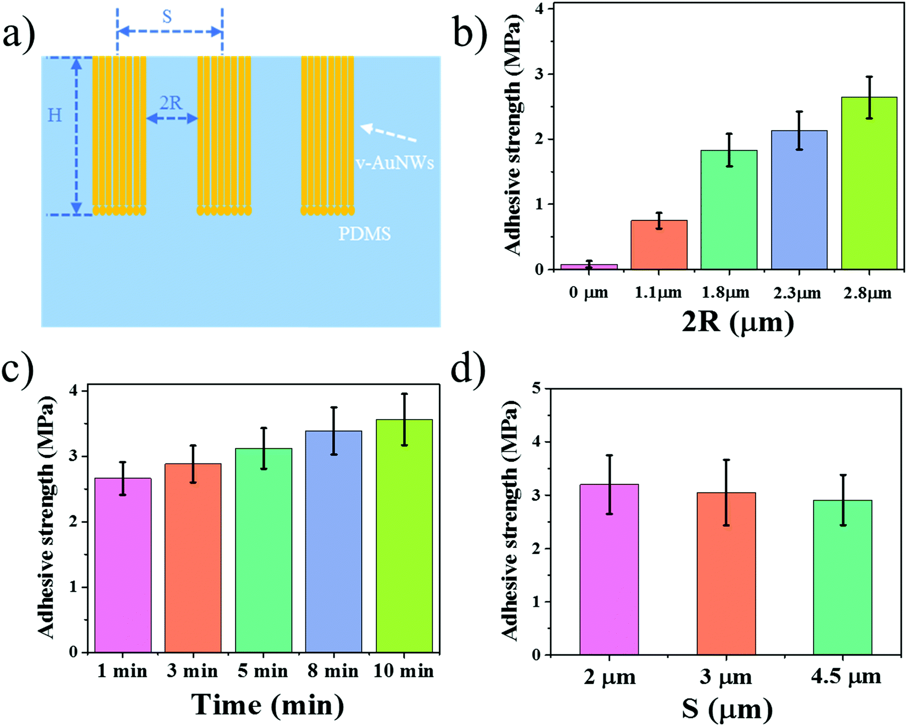 | ||
| Fig. 3 The adhesive strength of the pinhole v-AuNW stretchable electrode. (a) Schematic illustration of the pinhole v-AuNW stretchable electrode with specific parameters including the height of the v-AuNWs (H), the diameter of the pinhole (2R) and the distance of two adjunct pinholes (S). (b) adhesive strengths of v-AuNWs on PDMS, and electrodes with different pinhole sizes; adhesive strengths of the pinhole v-AuNW stretchable electrode. (c) The v-AuNWs were grown for different times, the height of the v-AuNWs was proportional to the growth time. (d) The distance between two adjunct pinholes. | ||
Moreover, we investigated how PS sphere diameter influenced the adhesive strength (Fig. 3d). It was known that heating duration would influence the pinhole sizes due to the heating-induced micromelting. Therefore, we applied 10 s heating for the three different PS microspheres (diameter: 2 μm, 3 μm and 4.5 μm). This led to comparable pinhole dimensions but with different pitch sizes (ESI,† Fig. S6). The results indicated that adhesive strength with 2 μm PS microspheres reached the highest value at 3.2 ± 0.55 MPa. This was attributed to higher number density of pinholes, hence, with more interfacial contact area between v-AuNWs and the PDMS substrate. Consequently, more friction had to be overcome in order to debond.
Since the pinholes in v-AuNWs promoted the overall film transparency (Fig. 2d and e), the relationship between the sheet resistance and the optical transmittance (wavelength of 550 nm) as a function of pinhole size were compared as shown in the ESI,† Fig. S7. The sheet resistance of the pinhole v-AuNWs/PDMS electrode with the pinhole diameter of 0.4 μm resulted in the lowest value of 5.2 Ω sq−1. When the pinhole diameter increased, both the sheet resistance and the optical transmittance increased, consistent with the expectation for enhanced transmission and reduced conductivity due to the lower material coverage.
Beyond the interfacial strength, we observed that the PDMS nails could also function as a means to tune the sensitivity of the stretchable electrode. In order to demonstrate this capability, we carried out a finite element analysis simulation by comparing a flat PDMS film, a small PDMS nail film and a large PDMS nail film. We found that the stress was redistributed if a suitable design was applied. As shown in Fig. 4a, stress was uniformly distributed among the entire PDMS film for flat PDMS under 20% strain. In contrast, the stress began to focus between two adjunct PDMS nails in a small PDMS nail film under the same strain. When the PDMS nail size was increased, more stress was further concentrated between two adjacent PDMS nails. SEM images in Fig. 4b and c also prove that nanocracks occurred in the small PDMS nail film while microcracks were developed in the large PDMS nail film because the large PDMS nails concentrated more stress compared with the small PDMS nails. To estimate the stretchable limit, pinhole v-AuNWs/PDMS electrodes with various pinhole sizes were stretched at a moving speed of 1 mm s−1 until conductivity was lost, as shown in Fig. 4d. v-AuNWs on PDMS could be stretched with a strain up to ∼70% before losing conductivity; in comparison, 2.8 μm pinhole v-AuNWs/PDMS electrode could only tolerate a strain up to ∼50%. The SEM images of dynamic stretching from 0% to 40% were used to investigate the interface between the v-AuNWs and substrate. As shown in the ESI,† Fig. S8 a to c, cracks formed and propagated along with the increasing strain and disappeared upon the release of strain. The cross-section view (ESI,† Fig. S8d) clearly demonstrated the interface where v-AuNWs were embedded in the PDMS substrate under a stretched state. The further durability test supported the high reproducibility of our stretchable electrode. There was no obvious deterioration in electrical responses under a 40% strain for 1000 stretching–releasing cycles, as shown in the ESI,† Fig. S9.
 | ||
| Fig. 4 (a) Stress distribution of PDMS film under 20% strain. Upper: Flat PDMS film; Middle: PDMS film with small nails; Bottom: PDMS film with large nails. SEM of the pinhole AuNWs/PDMS electrode with (b) small PDMS nails and (c) large PDMS nails under 20% strain. (d) Strain limitations and (e) dynamic stretching performances for a variety of pinhole v-AuNWs/PDMS stretchable electrodes. (f) Sensitivity of the pinhole v-AuNWs/PDMS stretchable electrode with various diameters of PDMS nails. (g) Radial pulse waves measured by D = 0 μm and D = 2.8 μm pinhole v-AuNWs/PDMS stretchable electrodes. | ||
Moreover, the stretchable electrode became more sensitive to external strains when pinhole structures were introduced. Fig. 4e shows that the 2.8 μm pinhole v-AuNWs/PDMS electrode exhibited the lowest stretchability but with the highest sensitivity. The gauge factor (GF) is defined as GF = ΔR/R0/Δε, where ΔR is the resistance change, R0 is the initial resistance and ε is the applied strain. A constant GF value of 28.6 was obtained for the 2.8 μm pinhole v-AuNWs/PDMS electrode, which was higher than the GFs for the 1.1 μm pinhole v-AuNWs/PDMS electrode (GF of 12.7) and for v-AuNWs grown on flat PDMS (GF of 10.2). The increasing trend of sensitivity with the increase of the pinhole size is evident as shown in Fig. 4f. This may be attributed to the decrease of the space between two adjacent PDMS nails, leading to stress concentration. The 2.8 μm pinhole v-AuNWs/PDMS electrode was sensitive enough to detect pulse waves, as shown in Fig. 4g. In comparison with v-AuNWs on PDMS, the 2.8 μm pinhole v-AuNWs/PDMS electrode yielded a ∼4 times enhanced amplitude, with each pulse showing more detailed physiological information including a systolic peak, diastolic peak and notch peak.16,35
It has to be noted that defects were unavoidable for self-assembling microsphere lithography. Nevertheless, the quality of microsphere arrays can be improved. We employed the reported unidirectional rubbing approach36,37 and obtained highly unformed assemblies (ESI,† Fig. S10). For an area of 5 cm × 6 cm, well-defined diffraction patterns formed by a commercial laser demonstrated the single-crystal domain on the PDMS surface.36 This may allow further improvement of the thin-layer nailing strategy reported here.
Conclusions
In summary, a woodwork nail-inspired microsphere lithography design was demonstrated for enhancing interfacial bonding between vertically aligned gold nanowires and elastomeric PDMS. By virtue of this design, we were able to enhance the adhesive strength up to about 24 times. Finite element modelling supported the stress-focusing effect of PDMS nails that was responsible for the higher sensitivity compared to the corresponding flat nanowire films. Microsphere lithography enabled efficient control over pinhole size, and hence, over the sensitivity of the resulting stretchable electrode. Using the microsphere lithography design, we were able to detect tiny biometric signals such as artery pulses. We believe that our fabrication strategy may open up a new route to design robust yet sensitive stretchable electrodes for applications in next-generation elastronics.Experimental
Materials and methods
![[thin space (1/6-em)]](https://www.rsc.org/images/entities/char_2009.gif) :7) for 30 min and then rinsed with DI water. 1 mL PS microsphere aqueous suspension (2.5% w/v) was centrifuged and 900 μL of supernatant was removed. A convective assembly setup was carried out to generate a PS microsphere array by coating 50 μL concentrated PS suspension on the pre-cleaned silicon wafer at a speed of 70 μm s−1. Note that it is difficult to assemble a perfect monolayer of PS microspheres over an area more than 2 × 2 cm2. However, double layers or multilayers of PS microspheres do not influence the quality and uniformity of the pinhole array, because the pinhole array only depends on the melted surface of the bottom PS microspheres. We also adopted the method of rubbing to fabricate monolayer PS microspheres, with reference to the previous ref. 36 and 37. The wafer with a PS microsphere array was then placed on a 110 °C hotplate for various durations in order to regulate the melting area between the silicon wafer and PS microspheres.
:1 by weight. After stirring, liquid PDMS was poured onto the as-prepared pinhole v-AuNWs wafer surface. To ensure successful transfer of v-AuNWs, the wafer was placed into a vacuum desiccator for 60 min to eliminate air bubbles. After heating at 60 °C for 2 h in an oven, the PDMS substrate was carefully peeled off. For the sample of v-AuNWs on PDMS, all the procedures are the same as for the pinhole v-AuNWs/PDMS stretchable electrode, except that the v-AuNW film was replaced with no pinhole structure.
:7) for 30 min and then rinsed with DI water. 1 mL PS microsphere aqueous suspension (2.5% w/v) was centrifuged and 900 μL of supernatant was removed. A convective assembly setup was carried out to generate a PS microsphere array by coating 50 μL concentrated PS suspension on the pre-cleaned silicon wafer at a speed of 70 μm s−1. Note that it is difficult to assemble a perfect monolayer of PS microspheres over an area more than 2 × 2 cm2. However, double layers or multilayers of PS microspheres do not influence the quality and uniformity of the pinhole array, because the pinhole array only depends on the melted surface of the bottom PS microspheres. We also adopted the method of rubbing to fabricate monolayer PS microspheres, with reference to the previous ref. 36 and 37. The wafer with a PS microsphere array was then placed on a 110 °C hotplate for various durations in order to regulate the melting area between the silicon wafer and PS microspheres.
:1 by weight. After stirring, liquid PDMS was poured onto the as-prepared pinhole v-AuNWs wafer surface. To ensure successful transfer of v-AuNWs, the wafer was placed into a vacuum desiccator for 60 min to eliminate air bubbles. After heating at 60 °C for 2 h in an oven, the PDMS substrate was carefully peeled off. For the sample of v-AuNWs on PDMS, all the procedures are the same as for the pinhole v-AuNWs/PDMS stretchable electrode, except that the v-AuNW film was replaced with no pinhole structure.
Conflicts of interest
There are no conflicts to declare.Acknowledgements
We acknowledge financial support from Australian Research Council via Discovery Grant scheme DP180101715 and Linkage Project LP160100521. This work was performed in part at the Melbourne Centre for Nanofabrication (MCN) in the Victorian Node of the Australian National Fabrication Facility (ANFF). Y. Ling thanks the financial aid from the Chinese Scholarship Council (CSC).Notes and references
- B. Zhu, S. Gong and W. Cheng, Chem. Soc. Rev., 2019, 48, 1668–1711 RSC.
- H. Kim, H. Lee, I. Ha, J. Jung, P. Won, H. Cho, J. Yeo, S. Hong, S. Han, J. Kwon, K. J. Cho and S. H. Ko, Adv. Funct. Mater., 2018, 28, 1801847 CrossRef.
- P. N. Chen, Y. F. Xu, S. S. He, X. M. Sun, S. W. Pan, J. Deng, D. Y. Chen and H. S. Peng, Nat. Nanotechnol., 2015, 10, 1077–1083 CrossRef CAS PubMed.
- S. Gong, W. Schwalb, Y. Wang, Y. Chen, Y. Tang, J. Si, B. Shirinzadeh and W. Cheng, Nat. Commun., 2014, 5, 3132 CrossRef PubMed.
- S. Choi, S. I. Han, D. Jung, H. J. Hwang, C. Lim, S. Bae, O. K. Park, C. M. Tschabrunn, M. Lee and S. Y. Bae, Nat. Nanotechnol., 2018, 13, 1048–1056 CrossRef CAS PubMed.
- Y. Qiang, P. Artoni, K. J. Seo, S. Culaclii, V. Hogan, X. Zhao, Y. Zhong, X. Han, P. M. Wang, Y. K. Lo, Y. Li, H. A. Patel, Y. Huang, A. Sambangi, J. S. V. Chu, W. Liu, M. Fagiolini and H. Fang, Sci. Adv., 2018, 4, eaat0626 CrossRef PubMed.
- Y. Q. Zhan, Y. F. Mei and L. R. Zheng, J. Mater. Chem. C, 2014, 2, 1220–1232 RSC.
- Z. Ma, P. Chen, W. Cheng, K. Yan, L. J. Pan, Y. Shi and G. H. Yu, Nano Lett., 2018, 18, 4570–4575 CrossRef CAS PubMed.
- J. Zhao, G. L. Wang, R. Yang, X. B. Lu, M. Cheng, C. L. He, G. B. Xie, J. L. Meng, D. X. Shi and G. Y. Zhang, ACS Nano, 2015, 9, 1622–1629 CrossRef CAS PubMed.
- H. H. Chou, A. Nguyen, A. Chortos, J. W. F. To, C. Lu, J. G. Mei, T. Kurosawa, W. G. Bae, J. B. H. Tok and Z. A. Bao, Nat. Commun., 2015, 6, 8011 CrossRef CAS PubMed.
- C. Y. Yan, W. B. Kang, J. X. Wang, M. Q. Cui, X. Wang, C. Y. Foo, K. J. Chee and P. S. Lee, ACS Nano, 2014, 8, 316–322 CrossRef CAS PubMed.
- N. N. Jason, M. D. Ho and W. L. Cheng, J. Mater. Chem. C, 2017, 5, 5845–5866 RSC.
- Z. F. He, W. J. Chen, B. H. Liang, C. Y. Liu, L. L. Yang, D. W. Lu, Z. C. Mo, H. Zhu, Z. K. Tang and X. C. Gui, ACS Appl. Mater. Interfaces., 2018, 10, 12816–12823 CrossRef CAS PubMed.
- S. C. B. Mannsfeld, B. C. K. Tee, R. M. Stoltenberg, C. V. H. H. Chen, S. Barman, B. V. O. Muir, A. N. Sokolov, C. Reese and Z. N. Bao, Nat. Mater., 2010, 9, 859–864 CrossRef CAS PubMed.
- Y. Q. Liu, K. He, G. Chen, W. R. Leow and X. D. Chen, Chem. Rev., 2017, 117, 12893–12941 CrossRef CAS PubMed.
- C. Dagdeviren, Y. W. Su, P. Joe, R. Yona, Y. H. Liu, Y. S. Kim, Y. A. Huang, A. R. Damadoran, J. Xia, L. W. Martin, Y. G. Huang and J. A. Rogers, Nat. Commun., 2014, 5, 4496 CrossRef CAS PubMed.
- X. Xiao, L. Y. Yuan, J. W. Zhong, T. P. Ding, Y. Liu, Z. X. Cai, Y. G. Rong, H. W. Han, J. Zhou and Z. L. Wang, Adv. Mater., 2011, 23, 5440–5444 CrossRef CAS PubMed.
- H. Ouyang, J. Tian, G. Sun, Y. Zou, Z. Liu, H. Li, L. Zhao, B. Shi, Y. Fan, Y. Fan, Z. L. Wang and Z. Li, Adv. Mater., 2017, 29, 1703456 CrossRef PubMed.
- S. Wagner and S. Bauer, MRS Bull., 2012, 37, 207–217 CrossRef.
- S. R. Ye, A. R. Rathmell, Z. F. Chen, I. E. Stewart and B. J. Wiley, Adv. Mater., 2014, 26, 6670–6687 CrossRef CAS PubMed.
- M. L. Hammock, A. Chortos, B. C. K. Tee, J. B. H. Tok and Z. A. Bao, Adv. Mater., 2013, 25, 5997–6037 CrossRef CAS PubMed.
- Z. Y. Liu, X. T. Wang, D. P. Qi, C. Xu, J. C. Yu, Y. Q. Liu, Y. Jiang, B. Liedberg and X. D. Chen, Adv. Mater., 2017, 29, 1603382 CrossRef PubMed.
- Y. X. Jin, D. Y. Deng, Y. R. Cheng, L. Q. Kong and F. Xiao, Nanoscale, 2014, 6, 4812–4818 RSC.
- H. M. Stec, R. J. Williams, T. S. Jones and R. A. Hatton, Adv. Funct. Mater., 2011, 21, 1709–1716 CrossRef CAS.
- Y. Wang, S. Gong, S. J. Wang, X. Y. Yang, Y. Z. Ling, L. W. Yap, D. S. Dong, G. P. Simon and W. L. Cheng, ACS Nano, 2018, 12, 9742–9749 CrossRef CAS PubMed.
- Y. Wang, S. Gong, D. Gomez, Y. Z. Ling, L. W. Yap, G. P. Simon and W. L. Cheng, ACS Nano, 2018, 12, 8717–8722 CrossRef CAS PubMed.
- Q. Zhai, Y. Wang, S. Gong, Y. Ling, L. W. Yap, Y. Liu, J. Wang, G. P. Simon and W. Cheng, Anal. Chem., 2018, 90, 13498–13505 CrossRef CAS PubMed.
- Y. Zhao, Q. Zhai, D. Dong, T. An, S. Gong, Q. Shi and W. Cheng, Anal. Chem., 2019, 91(10), 6569–6576 CAS.
- T. C. An, Y. Z. Ling, S. Gong, B. W. Zhu, Y. M. Zhao, D. S. Dong, L. W. Yap, Y. Wang and W. L. Cheng, Adv. Mater. Technol., 2019, 4, 1800473 CrossRef.
- D. F. Liu, Y. J. Xiang, X. C. Wu, Z. X. Zhang, L. F. Liu, L. Song, X. W. Zhao, S. D. Luo, W. J. Ma, J. Shen, W. Y. Zhou, G. Wang, C. Y. Wang and S. S. Xie, Nano Lett., 2006, 6, 2375–2378 CrossRef CAS PubMed.
- H. F. Tseng, M. H. Cheng, K. S. Jeng, J. W. Li and J. T. Chen, Macromol. Rapid Commun., 2016, 37, 1825–1831 CrossRef CAS PubMed.
- Y. W. Wang, J. T. He, S. Z. Yu and H. Y. Chen, Small, 2016, 12, 930–938 CrossRef CAS PubMed.
- J. T. He, Y. W. Wang, Y. H. Feng, X. Y. Qi, Z. Zeng, Q. Liu, W. S. Teo, C. L. Gan, H. Zhang and H. Y. Chen, ACS Nano, 2013, 7, 2733–2740 CrossRef CAS PubMed.
- D. P. Qi, Z. Y. Liu, Y. Liu, Y. Jiang, W. R. Leow, M. Pal, S. W. Pan, H. Yang, Y. Wang, X. Q. Zhang, J. C. Yu, B. Li, Z. Yu, W. Wang and X. D. Chen, Adv. Mater., 2017, 29, 1702800 CrossRef PubMed.
- Y. Park, J. Shim, S. Jeong, G. R. Yi, H. Chae, J. W. Bae, S. O. Kim and C. Pang, Adv. Mater., 2017, 29, 1606453 CrossRef PubMed.
- C. Park, T. Lee, Y. N. Xia, T. J. Shin, J. Myoung and U. Jeong, Adv. Mater., 2014, 26, 4633–4638 CrossRef CAS PubMed.
- K. Koh, H. Hwang, C. Park, J. Y. Lee, T. Y. Jeon, S. H. Kim, J. K. Kin and U. Jeong, ACS Appl. Mater. Interfaces, 2016, 8, 28149–28158 CrossRef CAS PubMed.
Footnote |
| † Electronic supplementary information (ESI) available: Supplementary figures, AFM, SEM images and tables. See DOI: 10.1039/c9nh00336c |
| This journal is © The Royal Society of Chemistry 2019 |