
Submillimeter and lead-free Cs3Sb2Br9 perovskite nanoflakes: inverse temperature crystallization growth and application for ultrasensitive photodetectors†
Zhi
Zheng‡
 a,
Qingsong
Hu‡
b,
Hongzhi
Zhou‡
c,
Peng
Luo
a,
Anmin
Nie
d,
Haiming
Zhu
c,
Lin
Gan
a,
Fuwei
Zhuge
a,
Ying
Ma
a,
Haisheng
Song
b and
Tianyou
Zhai
*a
a,
Qingsong
Hu‡
b,
Hongzhi
Zhou‡
c,
Peng
Luo
a,
Anmin
Nie
d,
Haiming
Zhu
c,
Lin
Gan
a,
Fuwei
Zhuge
a,
Ying
Ma
a,
Haisheng
Song
b and
Tianyou
Zhai
*a
aState Key Laboratory of Material Processing and Die & Mould Technology, School of Materials Science and Engineering, Huazhong University of Science and Technology (HUST), Wuhan 430074, Hubei, P. R. China. E-mail: zhaity@hust.edu.cn
bWuhan National Laboratory for Optoelectronics (WNLO) and School of Optical and Electronic Information, Huazhong University of Science and Technology (HUST), Wuhan 430074, Hubei, P. R. China
cCentre for Chemistry of High-Performance and Novel Materials, Department of Chemistry and State Key Laboratory of Modern Optical Instrumentation, Zhejiang University, Hangzhou 310027, Zhejiang, P. R. China
dCenter for High Pressure Science, State Key Laboratory of Metastable Materials Science and Technology, Yanshan Unversity, Qinhuangdao 066004, Hebei, P. R. China
First published on 29th July 2019
Abstract
Lead-free Cs3Sb2Br9 perovskites demonstrate wide applications in photodetectors owing to their remarkable optical properties and nontoxicity. Herein, we utilized an inverse temperature crystallization strategy to synthesize submillimeter Cs3Sb2Br9 perovskite nanoflakes. The carrier relaxation dynamics was investigated. Moreover, the Cs3Sb2Br9 perovskite nanoflake device exhibits fast response speed, high responsivity and excellent detectivity.
New conceptsLead halide perovskites with remarkable optical and electrical properties are widely applied in optoelectronics. However, lead is poisonous to the environment and humans, which hinders their further applications. Herein, we utilize antimony (Sb3+) substitution of lead (Pb2+) to synthesize submillimeter Cs3Sb2Br9 perovskite nanoflakes. A substrate-independent inverse temperature crystallization method was demonstrated to grow submillimeter level (>100 μm) and monocrystalline Cs3Sb2Br9 perovskite nanoflakes. The in-plane size can be controlled by adjusting the evaporating temperature and solute concentration. The band edge carrier relaxation processes including carrier trapping, electron–hole radiative recombination and Auger recombination based on Cs3Sb2Br9 perovskite nanoflakes were investigated. The fabricated Cs3Sb2Br9 nanoflake photodetector demonstrated high performance including fast response speed (24/48 ms), high responsivity (3.8 A W−1) and excellent detectivity (2.6 × 10¹² Jones). The developed submillimeter and lead-free Cs3Sb2Br9 perovskite nanoflakes promise great potential for fabricating high-performance optoelectronic devices. |
APbX3 (A: Cs, CH3NH3, X: Cl, Br, I) based all-inorganic perovskites demonstrate excellent optoelectronic properties including long carrier diffusion length, high carrier mobility and chemical stability.1–8 However, Pb compounds are toxic to humans and the environment.9 They may cause brain-related symptoms such as memory problems when accumulating in the human body; owning to their high solubility in water, they could also threaten the local biological system at a high risk.10 It is therefore highly desirable to replace Pb with a less toxic metal before advancing for commercialization of perovskites.
Lead-free halide perovskites based on lead substitution, such as Sb(III), and Bi(III), showed much lower toxicity.11–17 In particular, Cs3Sb2Br9 perovskites with the Sb(III) substitution of Pb(II), demonstrated a high absorption coefficient (>105 cm−1), small effective masses (me: 0.34, mh: 0.42), and direct band gap (2.4 eV).18 At present, QDs, bulk crystals or polycrystalline thin films based on lead-free halide perovskites have been reported through common synthesis methods such as liquid reprecipitation, co-evaporation or spin-coating.19–24 However, QDs or bulk crystals involve further complex device fabrication processes, leading to the high-cost of large-size assembly; polycrystalline thin films have high density of grain boundary defects, which are not beneficial to boost device performance. Large-size monocrystalline thin films are compatible with device integration. Moreover, they have lower bulk defects and longer carrier lifetime, and the high purities and superior carrier transport behaviors allow for the excited carriers to drift the device directly and quickly.25,26 Therefore, developing an efficient approach to synthesize large-size monocrystalline and lead-free halide perovskite thin films is highly desirable but remains a tremendous challenge.
Herein, we present an inverse temperature crystallization (ITC) method for synthesizing submillimeter-size monocrystalline lead-free Cs3Sb2Br9 perovskite nanoflakes (CPN). By tuning the evaporation temperatures and solute concentrations, we are able to control the morphology of the lead-free nanoflakes. In addition, the low-temperature photoluminescent (PL) and carrier dynamic process are revealed. The CPN device exhibits outstanding photodetecting performances such as high responsivity and detectivity.
Fig. 1 depicts the ITC synthesis process for CPN. Firstly, cesium bromide (CsBr) and antimony bromide (SbBr3) were dissolved in hybrid hydro bromic (HBr/H2O) at 403 K. Then, a drop of precursor solution was dripped onto the quartz substrate when the solution displayed a transparent and yellow color (Fig. 1a). The CPN were obtained via evaporating HBr hybrid solution at 413 K. This crystallization process is schematically illustrated in Fig. 1b. In hybrid HBr solution, dissociative Br atoms of CsBr attached to the extended SbBr3 octahedral network as terminal groups, allowing the formation of a typical hexagonal cell structure as the reaction proceeded. As the corner-sharing (Sb2Br9)3− network extended, CPN were formed. The unit cell crystal structure of CPN is similar to a traditional APbX3 crystal structure as schematically described in Fig. 1c. Cs3Sb2Br9 perovskites were made up of distorted and corner-sharing (SbBr6)3− octahedra, ten Cs cations encircled the dioctahedron (Sb2Br9)3− clusters.19 For the growth of CPN in HBr hybrid solution, two factors determine the growth rate: (1) the deposition rate of CsBr and SbBr3 solute molecules from solution onto the Cs3Sb2Br9 crystal surface; (2) the diffusion rate of CsBr and SbBr3 solute molecules from the crystal's surface into HBr hybrid solution.27 The diffusion rate shows an exponential increase as the temperature increases according to eqn (1):
 | (1) |
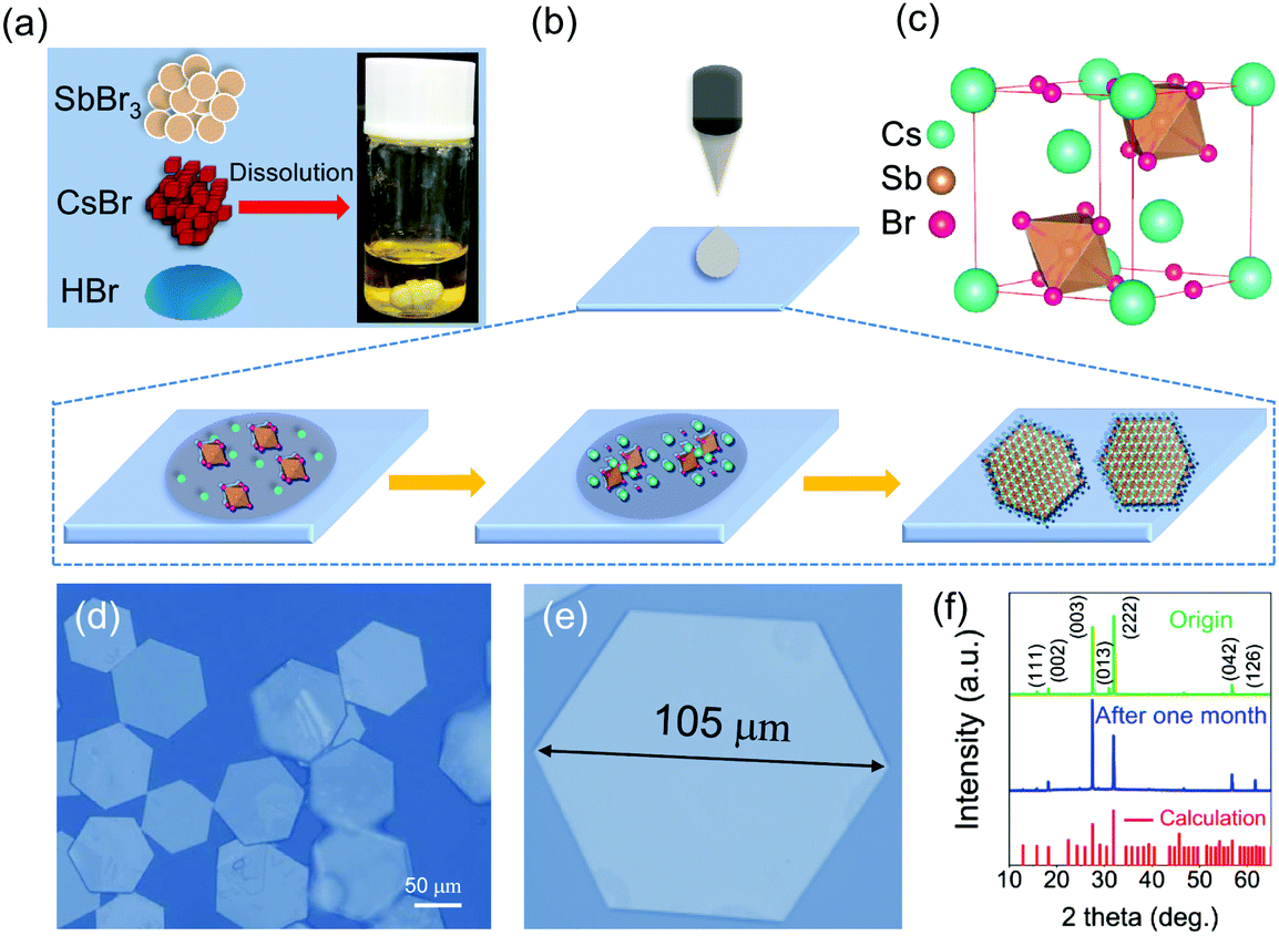 | ||
| Fig. 1 (a) Schematically illustrated dissolution process. (b) Schematically illustrated growth process of CPN. (c) The crystal structure of CPN. (d and e) Optical images for CPN grown on quartz substrates. (f) XRD patterns for freshly prepared CPN and after storage in moist air for one month. The bottom red lines are calculated patterns using CIF card (ICSD#39824). | ||
The importance of HBr for synthesis of CPN was also investigated as shown in Fig. S2 (ESI†). Only random CsBr particles were obtained in the pure water solution (without adding HBr) (Fig. S2a and d, ESI†). This result demonstrates that HBr facilitates the nucleation of Cs3Sb2Br9 clusters.28 Other polar solvents, such as dimethyl formamide (DMF) and dimethylsulfoxide (DMSO), were also used to synthesize CPN. However, they were not as effective as HBr in morphology control, and large particles (Fig. S2b and c, ESI†) with impurity peaks appeared in the final products (Fig. S2e and f, ESI†). The in-plane size and thickness of the pre-synthesized flakes were first characterized through optical microscope (OM) and atomic force microscope (AFM). The in-plane size of a typical nanoflake was around 105 μm (Fig. 1e and Fig. S3 (ESI†)), and its thickness was 90 nm (Fig. S4 (ESI†)). In addition, the obtained CPN exhibit hexagonal P![[3 with combining macron]](https://www.rsc.org/images/entities/char_0033_0304.gif) m1 symmetry referring to the calculated patterns using the CIF card of Cs3Sb2Br9 single crystals through vesta software (Fig. 1f). The main strong peaks of the (222) plane show that this was the preferred growth orientation. This conclusion corresponds to a hexagonal perovskite structure. In order to investigate the stability measurement of CPN, we stored the sample in a constant humidity (50%, 298 K) for one month. The XRD of the stored sample is similar to the fresh one and maintains the main crystal planes including (003) and (222) as shown in Fig. 1f, demonstrating the high water-resistant stability of these CPN.
m1 symmetry referring to the calculated patterns using the CIF card of Cs3Sb2Br9 single crystals through vesta software (Fig. 1f). The main strong peaks of the (222) plane show that this was the preferred growth orientation. This conclusion corresponds to a hexagonal perovskite structure. In order to investigate the stability measurement of CPN, we stored the sample in a constant humidity (50%, 298 K) for one month. The XRD of the stored sample is similar to the fresh one and maintains the main crystal planes including (003) and (222) as shown in Fig. 1f, demonstrating the high water-resistant stability of these CPN.
Importantly, submillimeter CPN can also be obtained on other substrates such as glass (100 μm, Fig. S5a (ESI†)) or PET (90 μm, Fig. S5b (ESI†)), indicating an excellent repeatability and convenience through this ITC strategy. Moreover, lead-free Cs3Bi2Br9 nanoflakes were also successfully synthesized through this strategy. The in-plane size and thickness of a typical nanoflake are about 50 μm and 150 nm, respectively (Fig. S6, ESI†), demonstrating a universality of this strategy.
The possible growth mechanism of submillimeter nanoflakes is explained as follows.29 Anions such as Br− and (Sb2Br9)3− in the droplet adsorb on the substrate surface to form an adlayer, serving as seed crystals as well as lowering the nucleation activation energy for Cs3Sb2Br9 growth. As HBr evaporates, the solution reaches the critical nucleation supersaturation. Cs3Sb2Br9 clusters nuclei on the substrate, leading to the decrease of the solute concentration at the solid–liquid interface. A driving force is established owning to this concentration gradient, leading to the diffusion of Cs+, Br− or (Sb2Br9)3− across the diffusion layers.30 The influence of solute concentration on the in-plane size was then investigated via supplementary experiments as shown in Fig. S7 (ESI†). The in-plane size of CPN increases as the CsBr solute concentration varies from 0.04 mmol L−1 to 0.08 mmol L−1 (Fig. S7a and b (ESI†)). Owning to the continuous supply of solute source, larger in-plane size of CPN was synthesized at higher concentration. However, an exorbitant concentration of CsBr and SbBr3 solute was not beneficial to obtain larger size of CPN.31
We measure the thickness of these nanoflakes under different evaporating temperatures and solute concentrations. The statistical result is shown in Fig. S8 (ESI†). The thickness of these nanoflakes decreases primarily as temperature and concentration increase, then increases as temperature and concentration continue to increase. This growth law of thickness is inverse to the variation of size, which was determined by the in-plane growth rate and vertical growth rate.32 For the synthesis at 0.08 mmol L−1 solute concentration, the thickness of CPN decreases as the temperature increases from 393 K to 413 K because the in-plane growth rate increases faster than the vertical growth rate. However, too high temperature will lead to growth along the vertical direction.33 It is reasonable that the thickness decreases as the solute concentration increases from 0.08 mmol L−1 to 0.12 mmol L−1 when synthesizing the CPN at 413 K, because the increase of concentration benefits the growth of nanoflakes both in-plane and in the vertical direction;34 the thickness of CPN increases when the concentration decreases from 0.08 mmol L−1 to 0.04 mmol L−1, which may result from the increase of in-plane growth rate.35
The key to realize high-performance photodetectors is to synthesize CPN with high crystalline quality. The hexagonal morphology of the low-magnification transmission electron microscopy (TEM) image is in accordance with its crystal structure while viewing from the [111] orientation (Fig. 2a). The 0.198 nm lattice distance is corresponding to the (02![[2 with combining macron]](https://www.rsc.org/images/entities/char_0032_0304.gif) 0) interplanar spacing of hexagonal Cs3Sb2Br9 (Fig. 2b). The related selected-area electron diffraction (SAED) pattern of CPN is shown in Fig. 2c. In a hexagonal crystal system, (020), (200) and (200) planes are equal to a (111) plane in a 4-axis coordinate system. The sharp edge and clear lattice fringe demonstrate a high-quality crystalline characteristic of CPN. Moreover, the detected Cs, Sb and Br counts in the energy dispersive X-ray spectroscopy (EDS) in Fig. S9 (ESI†) confirm the composition of the CPN, and their uniform distributions were demonstrated by the EDS mapping images (Fig. 2d–f).
0) interplanar spacing of hexagonal Cs3Sb2Br9 (Fig. 2b). The related selected-area electron diffraction (SAED) pattern of CPN is shown in Fig. 2c. In a hexagonal crystal system, (020), (200) and (200) planes are equal to a (111) plane in a 4-axis coordinate system. The sharp edge and clear lattice fringe demonstrate a high-quality crystalline characteristic of CPN. Moreover, the detected Cs, Sb and Br counts in the energy dispersive X-ray spectroscopy (EDS) in Fig. S9 (ESI†) confirm the composition of the CPN, and their uniform distributions were demonstrated by the EDS mapping images (Fig. 2d–f).
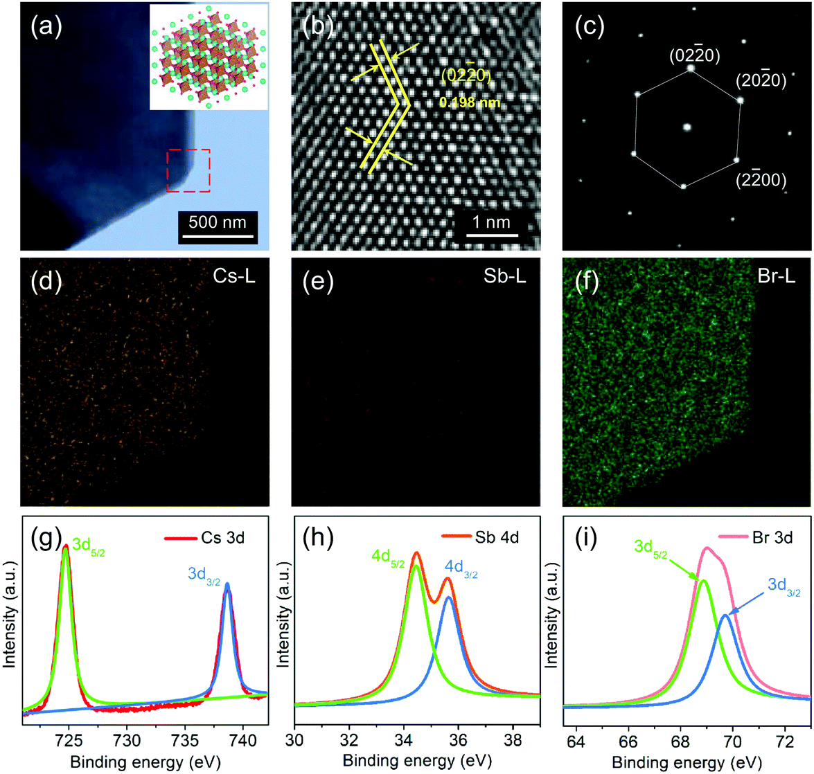 | ||
| Fig. 2 (a) TEM image of CPN. Inset is the crystal structure of CPN viewed from the [111] orientation. (b) HRTEM image of CPN. (c) SAED pattern of CPN. (d–f) EDS mapping of Cs, Sb, and Br, respectively. (g–i) XPS of Cs, Sb, and Br, respectively. | ||
To investigate the valence state and component of this CPN, the X-ray photoelectron spectroscopy (XPS) of single Cs3d, Sb4d and Br3d was collected as shown in Fig. 2g–i, respectively. The strong peaks at around 724.5 eV and 738.5 eV are from Cs3d5/2 and Cs3d3/2, respectively. While the couple peaks located at 34.5 eV and 35.6 eV are attributed to Sb4d5/2 and Sb4d3/2. For Br3d5/2 and Br3d3/2 of Br3d, the prominent peaks are located at around 68.9 eV and 69.7 eV, respectively. These peak positions of Cs3d, Sb4d and Br3d are verified by the reported values of Cs3Sb2Br9 QDs.19 According to the analytical results of OM, AFM, XRD, HRTEM and XPS, large size and highly crystalline CPN were successfully synthesized through the ITC growth strategy.
To investigate the optical properties of the CPN, the photoluminescence (PL) and UV-vis absorption properties were recorded as shown in Fig. 3. As the incident wavelength sweeps from 450 nm to 700 nm, the reflectance curve shows a sharp rising step from 450 nm to 515 nm, and displays a stable horizontal line when the incident light is longer than 515 nm (Fig. 3a). This increase of reflectance results from the increased light absorption coinciding with the band-gap of Cs3Sb2Br9. The optical band-gap can be investigated by the Kubelka–Munk equation as follows:
| αhν = A(hν − Eg)n | (2) |
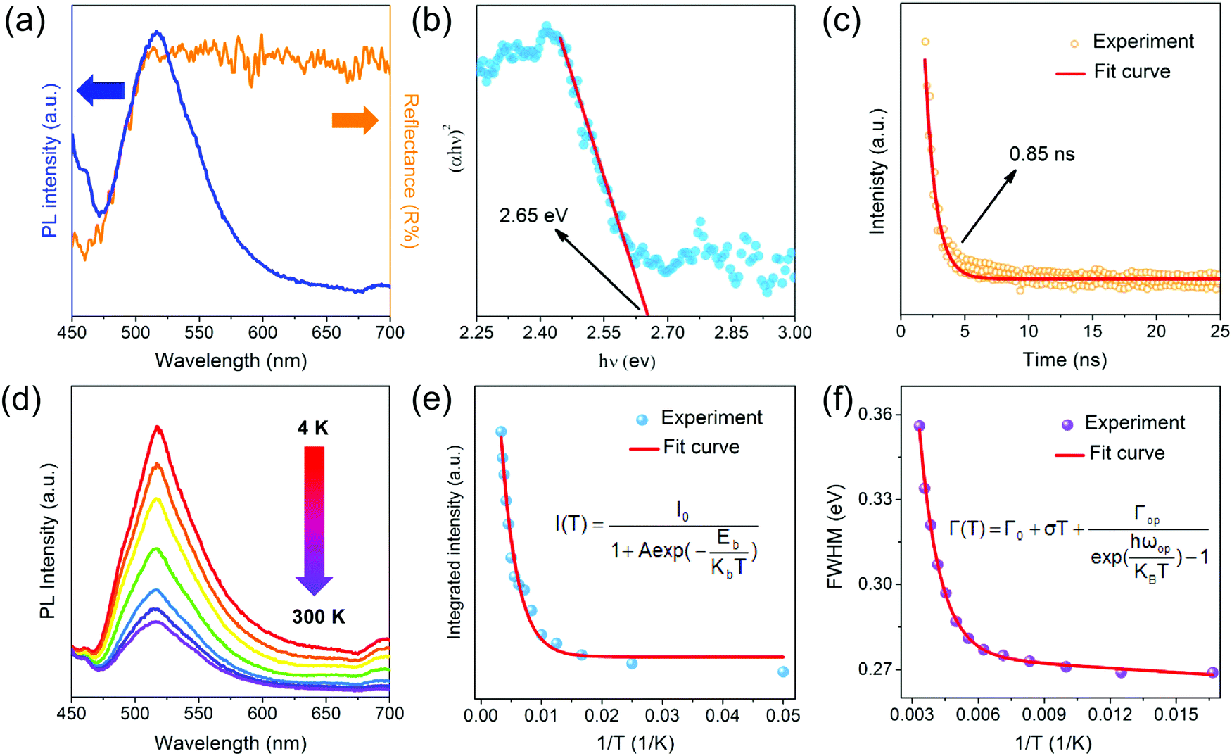 | ||
| Fig. 3 (a) PL spectrum and UV-vis diffuse reflectance spectrum of CPN. (b) The plot of (αhν)2 and hν. (c) Lifetime curve of CPN. (d) Measured PL spectra of CPN when increasing the temperature from 4 K to 300 K. (e–f) Temperature dependent integrated PL intensity and FWHM curves, respectively. The solid lines are fitted curves. | ||
Detailed information about both carrier relaxation processes and rate constants in the CPN was investigated through ultrafast transient reflection (TR) measurements. In the TR experiment, we focused both a 450 nm pump pulse and white light probe pulse on a single CPN using a microscope objective. We tested the sample by above the gap excitation and measured the reflectance change of broadband white light after a certain time delay (Fig. 4a). Fig. 4b shows the pseudo-color plot of representative TR spectra of a CPN with a few selected TR spectra at indicated delay times shown in Fig. 4c. The TR spectra showed a derivative-like spectral shape with a node at ∼545 nm, which can be ascribed to the carrier occupation induced band filling and associated reflectance change, similar to previous reported TR spectra of lead bromide single crystals.42 The TR signal reflects the photoexcited carrier population and its decay kinetics directly yielding the carrier recombination process in CPN. The TR kinetics of a single CPN at different photoexcited densities, (1.8–9.0) × 1018 cm−3, are shown in Fig. 4d. The TR signal decays faster with increasing carrier density and can be described by the following equation43
| dn/dt = −k1n − k2n2 − k3n3 | (3) |
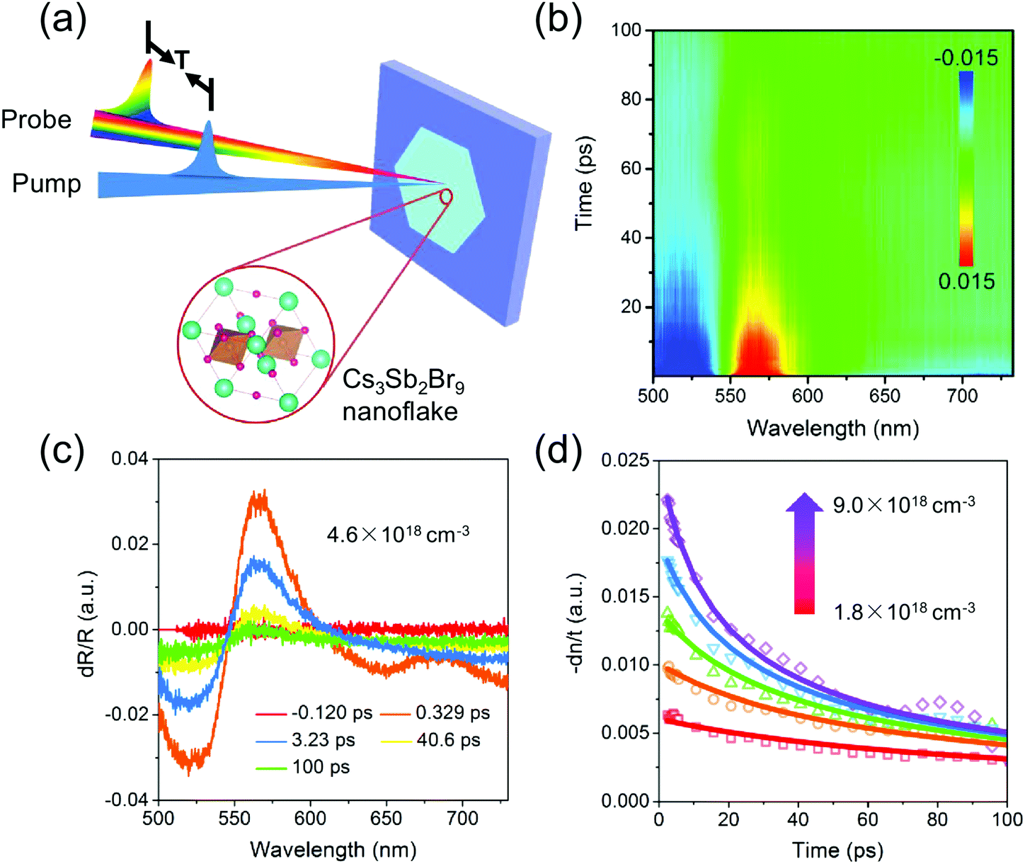 | ||
| Fig. 4 (a) The schematic diagram of TR measurements. (b) Pseudo color TR plot of CPN pumped by 450 nm pulse light with 4.6 × 1018 cm−3 photoexcited density. (c) TR spectra at the indicated delay time from −0.12 ps to 790 ps. (d) TR kinetics at various photoexcited densities, (1.8–9.0) × 1018 cm−3. Solid lines represent fits with a 1st, 2nd- and 3rd-order decay function described in the main text. | ||
To systematically explore the photodetecting properties of CPN, we fabricate the CPN device through a dry transfer strategy as described in the experimental section.48 The device illuminated under monochromatic light is shown in Fig. 5a. The width and length of the device channel are about 5 μm and 20 μm, respectively (Fig. S11 (ESI†)). The photoresponse of the device in the dark and under illumination of wavelengths ranging from 300 to 600 nm was first studied. Every single current–voltage (I–V) curve exhibits straight shape, suggesting a good Ohmic contact of the device. Moreover, the device undergoing on–off illumination of the above wavelengths is shown in Fig. 5b. A photocurrent can be clearly observed when the device was excited by the light wavelength shorter than 600 nm. The photocurrent of the device increases as the light wavelengths increase from 300 nm to 450 nm, then decreases as the light wavelength goes on increasing to 600 nm. The photocurrent reaches the largest value (3.0 nA) under 450 nm light illumination, consistent with the UV-vis diffuse reflectance curve shown in Fig. 3a. Fig. 5c demonstrates the switching stability of a photoresponse under 450 nm light illumination in CPN devices. After 5 cycles of a switching test, the device still shows unfailing photoresponse current and speed, confirming the excellent stability of the device. The detailed response process of the device was investigated by extracting a single on/off cycle. The response and decay time of CPN could be calculated as about 48 ms and 24 ms, respectively. Moreover, the photoresponse under irradiation at 450 nm light upon various powers is shown in Fig. 5d. The relationship between photocurrent and incident light power can be fitted with a power law (Fig. 5e). The θ can be calculated as 0.52, corresponding to the generation, separation, trapping and recombination processes of photo-generated electron–holes in the CPN.49 As shown in Fig. 5f, the responsivity of the device ranges from 3.8 A W−1 to 1.1 A W−1 as the light power increases from 0.289 mW cm−2 to 2.79 mW cm−2. The detectivity (D*) shows a similar decreased regularity from 2.6 × 10¹² Jones to 7.4 × 10¹¹ Jones as the light power increases from 0.289 mW cm−2 to 2.79 mW cm−2.50 Compared to the performance of other devices based on perovskite nanoplates in Table S1 (ESI†), the lead-free CPN device demonstrates a comparable high responsivity and excellent weak light detecting ability.
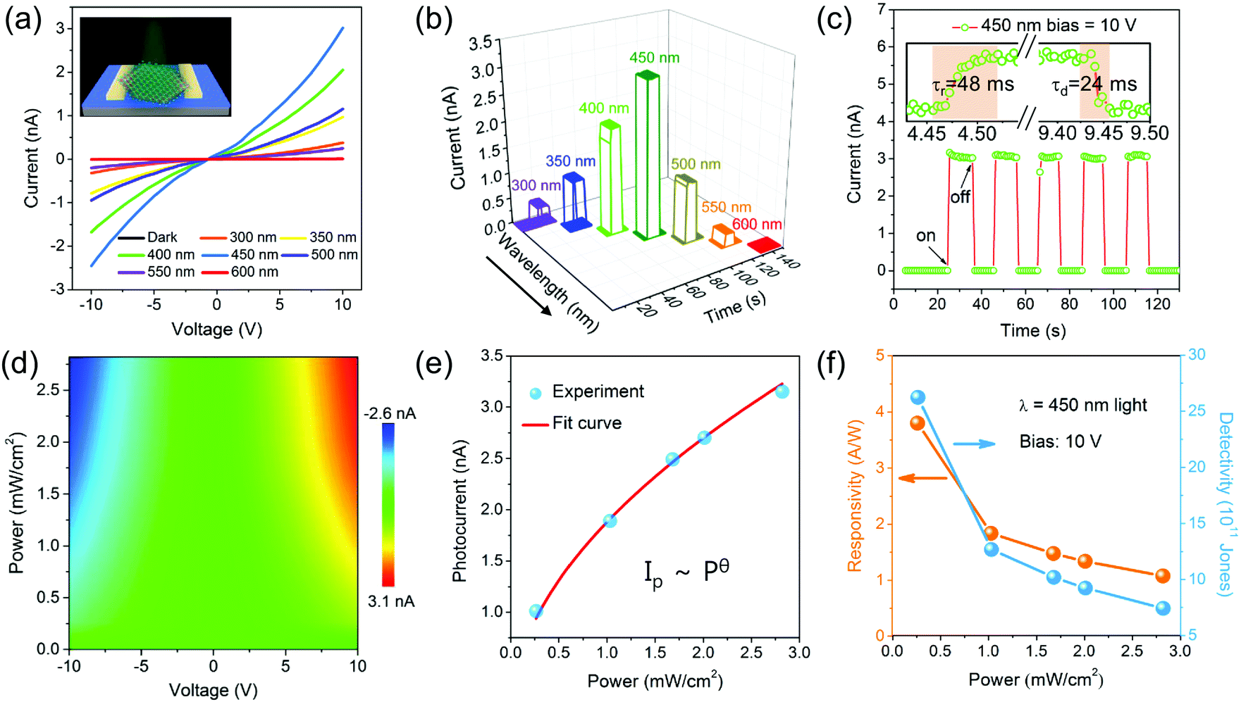 | ||
| Fig. 5 (a) I–V curves of the CPN device in the dark and under illumination of light wavelengths ranging from 300 to 600 nm. (b) 3D I–t curves of the device under illumination of 300–600 nm wavelength light, respectively. (c) I–t curve of the device for on–off tests under 450 nm light, inset is a single on/off cycle measurement. (d) 2D Pseudo color of I–V curves illuminated under 450 nm light with power intensities ranging from 0.289 to 2.79 mW cm−2. (e) Power dependent photocurrent curve and the corresponding power law fit curve under 450 nm light illumination. (f) Power dependent responsivity and detectivity curves under 450 nm light illumination. | ||
Conclusions
In summary, a facile ITC strategy is demonstrated for the growth of submillimeter and lead-free CPN. Moderate evaporating temperature and solute concentration are verified to control the in-plane size of the lead-free nanoflakes. The prepared CPN demonstrate comparable long lifetime (0.85 ns) and radiative and Auger recombination rate constants (2.9 × 10⁻⁹ cm3 s−1 and 8.8 × 10⁻²⁸ cm6 s−1). These superior intrinsic optical and electrical characteristics endow the Cs3Sb2Br9 based photodetectors with a fast respond speed (24/48 ms), high responsivity (3.8 A W−1), high photodetecting sensitivity (2.6 × 10¹² Jones), and good repeatable characteristics. Excellent photodetecting performance of the CPN as well as the facile synthetic approach may speed up the fabrication of large-size lead-free all-inorganic perovskite nanoflakes for future optoelectronic applications.Experimental
Synthesis of CPN
CPN were achieved through an ITC method. Firstly, CsBr and SbBr3 powder mixtures with a 3![[thin space (1/6-em)]](https://www.rsc.org/images/entities/char_2009.gif) :2 mole ratio were dissolved in 5 ml solvent such as 40% HBr (in water), DMF or DMSO. Then the solution was stirred and heated at 403 K. The color of the available uniform solution should be transparent and yellow. We dripped the precursor solution onto the substrate (quartz, glass, PET) heated at 393–433 K. After minutes of evaporation, final nanoflakes were obtained.
:2 mole ratio were dissolved in 5 ml solvent such as 40% HBr (in water), DMF or DMSO. Then the solution was stirred and heated at 403 K. The color of the available uniform solution should be transparent and yellow. We dripped the precursor solution onto the substrate (quartz, glass, PET) heated at 393–433 K. After minutes of evaporation, final nanoflakes were obtained.
Characterization of structure and morphology
An optical microscope (BX51, OLMPUS) and a field-emission scanning electron microscope (Quanta650 FEG, FEI) were used to monitor the morphology of the CPN. The thickness and superficial morphology were measured by an atomic force microscope (Dimension Icon, Bruker). The crystal structure of CPN was analyzed by powder X-ray diffraction (XRD) (Empyrean, PANalytical B.V.). The microstructure was further characterized by transmission electron microscope (Tecnai G2 F30, FEI).Characterization of optical properties
The diffuse reflectance and the electronic structure were recorded by a UV-vis spectrophotometer (U-3900H, Hitachi) and X-ray photoelectron spectroscope (AXIS-ULTRA DLD-600W, Kratos). Furthermore, the PL decay curve was measured by confocal Raman spectroscopy (ALPHA300 RAS, WITec) with a pulsing 355 nm laser. The PL property measurements including temperature range 4–300 K were performed using a fluorescence spectrometer (FLS980, Edinburgh). The band edge carrier relaxation processes were investigated based on the ultrafast transient reflection system. Two light beams separated from a Yb:KGW laser (Pharos, Light Conversion Ltd) function as seed light for the pump beam (450 nm, pulse duration ∼35 fs) and probe beam, respectively. Both beams reached the pump–probe spectrometer colinearly (mFemtoTR100, Time-tech Spectra) and were focused into a cycloidal beam size with 0.4 μm diameter. The reflected probe light before and after pumping on the sample was collected by EMCCD (Princeton Instruments). The delay time was controlled through a delay stage (Newport).Fabrication of CPN photodetector
The CPN device was fabricated using a dry-transfer strategy. Firstly, the blank electrodes (10 nm Ti/90 nm Au) with 5 μm channel were fabricated on the SiO2/Si substrate through a traditional photolithographic process. Afterwards, a small piece of PVA thin film was used to stick the CPN grown on the quartz substrate. Then, the PVA film with CPN was transferred onto pre-fabricated electrodes under a microscope.Photodetection measurements
The optoelectronic measurements including I–V and I–t curves were performed using a low-temperature cryogenic probe station (CRX-6.5K, Lake Shore) combined with a semiconductor parameter analyzer (4200-SCS, Keithley). The monochromatic light in the range of 300–600 nm was split from a white light source (LDLS, EQ-1500, Energetiq). Moreover, the different power intensities for 450 nm light were realized through changing the size of the spot area. The power intensities were calibrated using a UV enhanced Si photodiode.Conflicts of interest
There are no conflicts to declare.Acknowledgements
This work was supported by the National Natural Science Foundation of China (21825103, 21801081, 51872100, and 51727809), the National Basic Research Program of China (2015CB932600), the National Key Research and Development Program of “Strategic Advanced Electronic Materials” (2016YFB0401100), and the China Postdoctoral Science Foundation (2017M622434), and the Fundamental Research Funds for the Central University (2019kfyXMBZ018). The authors thank the Analytical and Testing Center of Huazhong University of Science and Technology (HUST) for providing XRD and HRTEM measurements.References
- M. Ahmadi, T. Wu and B. Hu, Adv. Mater., 2017, 29, 1605242 CrossRef PubMed.
- F. P. G. de Arquer, A. Armin, P. Meredith and E. H. Sargent, Nat. Rev. Mater., 2017, 2, 1 Search PubMed.
- X. He, P. Liu, H. Zhang, Q. Liao, J. Yao and H. Fu, Adv. Mater., 2017, 29, 1604510 CrossRef PubMed.
- S. Chen, K. Roh, J. Lee, W. K. Chong, Y. Lu, N. Mathews, T. C. Sum and A. Nurmikko, ACS Nano, 2016, 10, 3959 CrossRef CAS PubMed.
- D. Shi, V. Adinolfi, R. Comin, M. Yuan, E. Alarousu, A. Buin, Y. Chen, S. Hoogland, A. Rothenberger, K. Katsiev, Y. Losovyj, X. Zhang, P. A. Dowben, O. F. Mohammed, E. H. Sargent and O. M. Bakr, Science, 2015, 347, 519 CrossRef CAS PubMed.
- F. Sahli, J. Werner, B. A. Kamino, M. Bräuninger, R. Monnard, B. Paviet-Salomon, L. Barraud, L. Ding, J. J. D. Leon, D. Sacchetto, G. Cattaneo, M. Despeisse, M. Boccard, S. Nicolay, Q. Jeangros, B. Niesen and C. Ballif, Nat. Mater., 2018, 17, 820 CrossRef CAS PubMed.
- N. Wang, L. Cheng, R. Ge, S. Zhang, Y. Miao, W. Zou, C. Yi, Y. Sun, Y. Cao, R. Yang, Y. Wei, Q. Guo, Y. Ke, M. Yu, Y. Jin, Y. Liu, Q. Ding, D. Di, L. Yang, G. Xing, H. Tian, C. Jin, F. Gao, R. H. Friend, J. Wang and W. Huang, Nat. Photonics, 2016, 10, 699 CrossRef CAS.
- Z. G. Xiao, R. A. Kerner, L. F. Zhao, N. L. Tran, K. M. Lee, T. W. Koh, G. D. Scholes and B. P. Rand, Nat. Photonics, 2017, 11, 108 CrossRef CAS.
- W. C. Pan, H. D. Wu, J. J. Luo, Z. Z. Deng, C. Ge, C. Chen, X. W. Jiang, W. J. Yin, G. D. Niu, L. J. Zhu, L. X. Yin, Y. Zhou, Q. G. Xie, X. X. Ke, M. L. Sui and J. Tang, Nat. Photonics, 2017, 17, 726 CrossRef.
- A. Babayigit, A. Ethirajan, M. Muller and B. Conings, Nat. Mater., 2016, 15, 247 CrossRef CAS PubMed.
- H. Liu, Z. Wu, J. Shao, D. Yao, H. Gao, Y. Liu, W. Yu, H. Zhang and B. Yang, ACS Nano, 2017, 11, 2239 CrossRef CAS PubMed.
- X. G. Zhao, J. H. Yang, Y. Fu, D. Yang, Q. Xu, L. Yu, S. H. Wei and L. Zhang, J. Am. Chem. Soc., 2017, 139, 2630 CrossRef CAS PubMed.
- M. Leng, Z. Chen, Y. Yang, Z. Li, K. Zeng, K. Li, G. Niu, Y. He, Q. Zhou and J. Tang, Angew. Chem., Int. Ed., 2016, 55, 15012 CrossRef CAS PubMed.
- T. C. Jellicoe, J. M. Richter, H. F. Glass, M. Tabachnyk, R. Brady, S. E. Dutton, A. Rao, R. H. Friend, D. Credgington, N. C. Greenham and M. L. Bohm, J. Am. Chem. Soc., 2016, 138, 2941 CrossRef CAS PubMed.
- T. Jun, K. Sim, S. Iimura, M. Sasase, H. Kamioka, J. Kim and H. Hosono, Adv. Mater., 2018, 30, 1804547 CrossRef PubMed.
- B. Yang, J. S. Chen, F. Hong, X. Mao, K. B. Zheng, S. Q. Yang, Y. J. Li, T. Pullerits, W. Q. Deng and K. L. Han, Angew. Chem., Int. Ed., 2017, 56, 12471 CrossRef CAS PubMed.
- C. C. Stoumpos, L. Frazer, D. J. Clark, Y. S. Kim, S. H. Rhim, A. J. Freeman, J. B. Ketterson, J. I. Jang and M. G. Kanatzidis, J. Am. Chem. Soc., 2015, 137, 6804 CrossRef CAS PubMed.
- B. Saparov, F. Hong, J.-P. Sun, H.-S. Duan, W. W. Meng, S. Cameron, I. G. Hill, Y. F. Yan and D. B. Mitzi, Chem. Mater., 2015, 27, 5622 CrossRef CAS.
- J. Zhang, Y. Yang, H. Deng, U. Farooq, X. K. Yang, J. Khan, J. Tang and H. S. Song, ACS Nano, 2017, 11, 9294 CrossRef CAS PubMed.
- M. B. Johansson, H. Zhu and E. M. J. Johansson, J. Phys. Chem. Lett., 2016, 7, 3467 CrossRef CAS PubMed.
- A. H. Slavney, L. Leppert, D. Bartesaghi, A. Gold-Parker, M. F. Toney, T. J. Savenije, J. B. Neaton and H. I. Karunadasa, J. Am. Chem. Soc., 2017, 139, 5015 CrossRef CAS PubMed.
- Y. Kim, Z. Yang, A. Jain, O. Voznyy, G. H. Kim, M. Liu, L. N. Quan, F. P. García de Arquer, R. Comin, J. Z. Fan and E. H. Sargent, Angew. Chem., Int. Ed., 2016, 55, 9586 CrossRef CAS PubMed.
- K. P. Marshall, M. Walker, R. I. Walton and R. A. Hatton, Nat. Energy, 2016, 1, 1 Search PubMed.
- I. Chung, B. Lee, J. He, R. P. H. Chang and M. G. Kanatzidis, Nature, 2012, 485, 486 CrossRef CAS PubMed.
- W. Nie, H. Tsai, R. Asadpour, J. C. Blancon, A. J. Neukirch, G. Gupta, J. J. Crochet, M. Chhowalla, S. Tretiak, M. A. Alam, H. L. Wang and A. D. Mohite, Science, 2015, 347, 522 CrossRef CAS PubMed.
- H. S. Rao, W. G. Li, B. X. Chen, D. B. Kuang and C. Y. Su, Adv. Mater., 2017, 29, 1602639 CrossRef PubMed.
- Y. C. Liu, Y. X. Zhang, Z. Yang, J. S. Feng, Z. Xu, Q. X. Li, M. X. Hu, H. C. Ye, X. Zhang, M. Liu, K. Zhao and S. Z. Liu, Mater. Today, 2019, 22, 67 CrossRef CAS.
- Q. A. Akkerman, S. G. Motti, A. R. S. Kandada, E. Mosconi, V. D’Innocenzo, G. Bertoni, S. Marras, B. A. Kamino, L. Miranda, F. D. Angelis, A. Petrozza, M. Prato and L. Manna, J. Am. Chem. Soc., 2016, 138, 1010 CrossRef CAS PubMed.
- M. V. Kelso, N. K. Mahenderkar, Q. Z. Chen, J. Z. Tubbesing and J. A. Switzer, Science, 2019, 364, 166 CAS.
- G. B. Stringfellow, Rep. Prog. Phys., 1982, 45, 469 CrossRef.
- M.-H. Sunga, J.-S. Kimb, W.-S. Kimc, I. Hirasawac and W.-S. Kim, J. Cryst. Growth, 2002, 235, 529 CrossRef.
- C. Y. Yan, L. Gan, X. Zhou, J. Guo, W. J. Huang, J. W. Huang, B. Jin, J. Xiong, T. Y. Zhai and Y. R. Li, Adv. Funct. Mater., 2017, 27, 1702918 CrossRef.
- Z. Zheng, X. X. Wang, Y. W. Shen, Z. Y. Luo, L. G. Li, L. Gan, Y. Ma, H. Q. Li, A. L. Pan and T. Y. Zhai, Adv. Opt. Mater., 2018, 6, 1800879 CrossRef.
- C. Xie, L. Xiao, M. Hu, Z. Bai, X. Xia and D. Zeng, Sens. Actuators, B, 2010, 145, 457 CrossRef CAS.
- M. H. Sung, J. S. Kim, W. S. Kim, I. Hirasawa and W. S. Kim, J. Cryst. Growth, 2002, 235, 529 CrossRef CAS.
- B. Yang, F. Y. Zhang, J. S. Chen, S. Q. Yang, X. S. Xia, T. Pullerits, W. Q. Deng and K. L. Han, Adv. Mater., 2017, 29, 1703758 CrossRef PubMed.
- Z. Zheng, X. X. Wang, Y. W. Shen, L. G. Li, Y. Ma, H. Q. Li, A. L. Pan and T. Y. Zhai, Adv. Opt. Mater., 2018, 6, 1800879 CrossRef.
- D. Das, S. L. Shinde and K. K. Nanda, ACS Appl. Mater. Interfaces, 2016, 8, 2181 CrossRef CAS PubMed.
- S. Zhang, Q. Y. Shang, W. N. Du, J. Shi, Z. Y. Wu, Y. Mi, J. Chen, F. J. Liu, Y. Z. Li, M. Liu, Q. Zhang and X. F. Liu, Adv. Opt. Mater., 2018, 6, 1701032 CrossRef.
- W. Zhang, M. Saliba, S. D. Stranks, Y. Sun, X. Shi, U. Wiesner and H. J. Snaith, Nano Lett., 2013, 13, 4505 CrossRef CAS PubMed.
- F. Zhang, H. Z. Zhong, C. Chen, X. G. Wu, H. M. Hu, H. L. Huang, J. B. Han, B. S. Zou and Y. P. Dong, ACS Nano, 2015, 9, 4533 CrossRef CAS PubMed.
- H. M. Zhu, M. T. Trinh, J. Wang, Y. P. Fu, P. P. Joshi, K. Miyata, S. Jin and X.-Y. Zhu, Adv. Mater., 2017, 29, 1603072 CrossRef PubMed.
- L. M. Herz, Annu. Rev. Phys. Chem., 2016, 67, 65 CrossRef CAS PubMed.
- M. Saba, M. Cadelano, D. Marongiu, F. Chen, V. Sarritzu, N. Sestu, C. Figus, M. Aresti, R. Piras, A. Geddo Lehmann, C. Cannas, A. Musinu, F. Quochi, A. Mura and G. Bongiovanni, Nat. Commun., 2014, 5, 1 Search PubMed.
- Q. Zhang, L. Q. Chu, F. Zhou, W. Ji and G. Eda, Adv. Mater., 2018, 30, 1704055 CrossRef PubMed.
- E. Shi, S. B. Deng, B. Yuan, Y. Gao, Akriti, L. Yuan, C. S. Davis, D. Zemlyanov, Y. Yu, L. B. Huang and L. T. Dou, ACS Nano, 2019, 13, 1635 CAS.
- C. Wehrenfennig, G. E. Eperon, M. B. Johnston, H. J. Snaith and L. M. Herz, Adv. Mater., 2014, 26, 1584 CrossRef CAS PubMed.
- C. X. Huo, X. H. Liu, X. G. Song, Z. M. Wang and H. B. Zeng, J. Phys. Chem. Lett., 2017, 8, 4785 CrossRef CAS PubMed.
- H. Kind, H. Q. Yan, B. Messer, M. Law and P. D. Yang, Adv. Mater., 2002, 14, 158 CrossRef CAS.
- J. Kim, J. Kim, S. Jo, J. Kang, J.-W. Jo, M. Lee, J. Moon, L. Yang, M.-G. Kim, Y.-H. Kim and S. K. Park, Adv. Mater., 2016, 28, 3078 CrossRef CAS PubMed.
Footnotes |
| † Electronic supplementary information (ESI) available. See DOI: 10.1039/c9nh00426b |
| ‡ These authors contributed equally to this work. |
| This journal is © The Royal Society of Chemistry 2019 |