
Band engineering realized by chemical combination in 2D group VA–VA materials†
Shiying
Guo
,
Wenhan
Zhou
,
Bo
Cai
,
Kan
Zhang
,
Shengli
Zhang
 * and
Haibo
Zeng
*
* and
Haibo
Zeng
*
Key Laboratory of Advanced Display Materials and Devices, Ministry of Industry and Information Technology, Nanjing University of Science and Technology, Nanjing, 210094, China. E-mail: zhangslvip@njust.edu.cn; zeng.haibo@njust.edu.cn
First published on 23rd April 2019
Abstract
Two-dimensional (2D) group VA materials share classical configurations, buckled and puckered honeycomb structures, with intriguing wide electronic properties that have attracted great research interest. The chemical combination of different group VA elements can realize the band engineering of 2D group VA materials owing to their distinct atomic radii and electronegativities. Based on first principles calculation, we present a detailed theoretical investigation of these 2D group VA–VA materials with buckled and puckered structures, including atomic structure, energy stability, and electronic properties. These 2D group VA–VA materials showed appreciable cohesive energies comparable to 2D group VA materials, and were semiconductors with a wide range of bandgaps from 0.49–2.82 eV. Seven of these materials showed an intrinsic direct bandgap. Interestingly, the bandgaps of the 2D group VA–VA materials showed a regular trend related to their atomic radii and electronegativities. In particular, Mexican-hat dispersion and Rashba spin splitting were present in the valence band and conduction band of the 2D buckled structures, respectively. Our comprehensive study further develops the 2D group VA materials family and provides promising candidates for optoelectronic and spintronic applications.
New conceptsTwo-dimensional (2D) group VA materials with buckled and puckered honeycomb structures have attracted great research interest owing to their intriguing electronic properties and wide applications. Herein, we conduct the chemical combination of different group-VA elements to realize the band engineering of 2D group VA materials. This tuning approach is supported by the diverse atomic radii and electronegativities of group VA elements. Through detailed calculations and LCAO analysis, we confirm that the electronic band structures of 2D group VA–VA materials show a regular evolution related to their atomic radii and electronegativities. Furthermore, among these 2D group VA–VA materials, seven showed an intrinsic direct bandgap with a suitable gap value. In particular, 2D buckled NX and XBi present special electronic structures, namely, Mexican-hat dispersion and Rashba spin splitting, in the valence and conduction bands, respectively. This theoretical study should promote further experimental realization of 2D group VA–VA materials to improve their potential for nanoelectronic and optoelectronic applications. |
Introduction
Two-dimensional (2D) materials have become the focus of intensive research owing to their outstanding properties, which are not found in their bulk counterparts.1–7 In particular, graphene, the most fundamental 2D material, has been extensively studied theoretically and experimentally.8 The Dirac cone in the electronic structure and exceptional magnetic properties of graphene strongly promote its further research in nanoelectronics.9,10 Group IVA materials beyond graphene have also been explored and found to possess electronic structures similar to graphene, such as silicene, germanene, and stanene.11 Recently, following the successful fabrication of phosphorene, 2D group VA materials, including phosphorene, have become significant members of the 2D materials family.12,13 Arsenene, antimonene, bismuthene, and phosphorene have appropriate bandgaps for electronics and optoelectronic devices.14–19 Interestingly, 2D group IVA and group VA materials are both composed of hexagonal units with three-coordinated atoms despite their valence electrons being arranged differently. Furthermore, 2D group IVA and group VA materials have three classic configurations: (i) planar; (ii) buckled; and (iii) puckered. These three configurations exhibit an array of fascinating quantum structures and various possibilities for exciting technological applications.The chemical combination of two different group VA elements, which have the same number of valence electrons, but different atomic radii and electronegativities, to fine-tune their electronic structures and further broaden their potential applications has received research interest. Recently, a photodetector based on 2D black arsenic phosphorus realized a fast mid-infrared photoresponse.20,21 The black arsenic phosphorus materials have fully tunable bandgaps and optical properties that cover long wavelengths down to around 0.15 eV.22 Sandwiched within hexagonal boron nitride to ensure long-term stability, the photodetector based on 2D black arsenic phosphorus covered a broad mid-infrared wavelength range of 3.4–7.7 μm.23 A bismuth–antimony compound was reported to show enhanced electrochemical cycling stability compared with pure Sb or Bi as anodes for sodium ion batteries.24 Furthermore, bismuth–antimony nanosheets have been shown to have a high carrier mobility and high bulk conductivity, which are promising for application as a spin current source in ultralow power spin–orbit torque random-access memory.25 Recent research has also demonstrated the potential of group VA binary compounds in photoelectric devices and spin electronics.26,27
In this study, using first principles calculation, we revealed the significance of atomic radii and electronegativity in constructing buckled and puckered structures of 2D group IVA and VA materials. Atomic radii and electronegativity also played important roles in the electronic properties of these 2D IVA and VA materials. Accordingly, we combined two distinct group VA elements into 2D group VA–VA materials to realize the band engineering of 2D group VA materials. These 2D group VA–VA materials with buckled and puckered structures had cohesive energies comparable to those of group VA materials, indicating their similar structural stability. We calculated the electronic structures of 2D group VA–VA materials using the PBE and HSE functionals. The bandgaps of the 2D group VA–VA materials showed a regular trend related to their atomic radii and electronegativities. Furthermore, we have described the energy band alignment of 2D group VA–VA materials, providing information for constructing heterostructures. In particular, special electronic structures, namely, Mexican-hat dispersion and Rashba spin splitting, were found in the valence and conduction bands of 2D buckled NX and XBi, respectively. Their novel electronic properties make these materials promising candidates for magnetic and spintronic nanodevices.
Computational methods
All calculations were based on density functional theory (DFT). Two-dimensional materials were calculated using the Vienna Ab initio Simulation Package (VASP) code. Ion–electron interactions were described using a projected augmented wave (PAW) approximation.28,29 The exchange–correlation functional was treated using the Perdew–Burke–Ernzerhof (PBE) form of the generalized gradient approximation (GGA).30 The spin–orbit coupling (SOC) effect was employed using a second-variation method implemented in VASP code. The HSE06 functional was used to describe more accurate band structures, especially the bandgap.31 For both the PBE and HSE06 functionals, the cutoff energy was set to 500 eV and the convergence thresholds were converged to 1 × 10⁻⁵ eV and 0.01 eV Å−1, respectively. The Brillouin zone was represented by 15 × 15 × 1 Monkhorst–Pack k-grids for geometric relaxation, and 21 × 21 × 1 for electronic properties based on the PBE and HSE06 functionals.32 For calculations on 2D systems, a vacuum space of 20 Å was applied to avoid interactions between two neighbor images. Geometry and electronic properties of small molecules were performed using Dmol3 code in Materials Studio based on the GGA-PBE method.33,34Results and discussion
As shown in Fig. 1a, 2D group IVA and VA monolayers had three types of geometric configurations, which have been confirmed as the minimum energy structures.11,15 These geometric structures are all comprised numerous hexagons with three-coordinated atoms, but present entirely different folds, namely, planar, buckled, and puckered structures. Graphene forms a perfect planar hexagonal lattice. Other group IVA monolayers, except graphene, and group VA monolayers shared the same buckled structure. Group VA monolayers also possessed another stable configuration, namely, a puckered structure.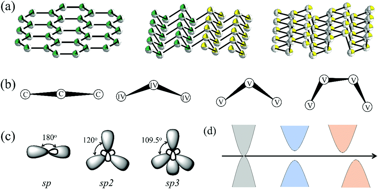 | ||
| Fig. 1 (a) Three classic geometric configurations for 2D group IVA and VA materials, namely, planar, buckled, and puckered structures. (b) Side views of 2D group IVA and VA materials. (c) Three types of orbital hybridization. (d) Three types of electronic structure. | ||
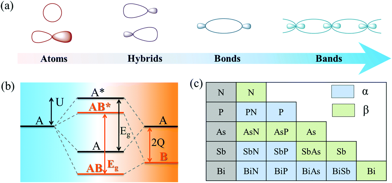 | ||
| Fig. 2 (a) Atomic schematic diagram and (b) energy level diagram for the linear combinations of solids from atomic orbitals, explaining band and bandgap formation in a monopolar crystal (A) and polar crystal (composite AB). 2Q, U, and Eg represent the energy difference between atomic orbitals, bonding interaction strength, and bandgap, respectively. (c) Stability comparison between two phases of group VA monolayers and group VA–VA monolayers. Phases α and β represent puckered and buckled structures, respectively. | ||
From the side views of these configurations in Fig. 1b, their structural characteristics were clearly distinguished. Carbon covalent bonds in graphene were provided by the overlap of sp2 hybridized orbitals, as shown in Fig. 1c. Three valence electrons of carbon form σ orbitals, while one valence electron occupies a pz orbital to form a delocalized π orbital with a neighboring atom. However, for other group IVA monolayers, silicene, germanene, and stanene, atoms in buckled structures were bonded through mixed sp2 and sp3 hybridization, corresponding to bond angles of between 120° and 109.5° (Table S1, ESI†). Group VA monolayers possessed a buckled structure similar to that of silicene, germanene, and stanene, but with smaller bond angles, mainly due to their different hybridized orbitals. One group VA atom formed sp3 hybridized orbitals owing to the five valence electrons. Three valence electrons participated in the formation of three σ bonds, while the other two electrons occupied a pz orbital as a lone pair. As shown in Table S1 (ESI†), the bond angles in the buckled group VA structures were smaller than the ideal tetrahedral angle of 109.5°, as explained by the repulsive interaction between the lone pair and bonding orbital. The same bonding situation existed in their puckered structures, with puckering causing anisotropy in their structures. There were three typical electronic structures, namely, a Dirac cone, direct bandgap, and indirect bandgap, among these classic configurations, as shown in Fig. 1d.
We selected hexagons passivated by hydrogen as the basic building block to aid further understanding of the properties in these three geometric configurations. As shown in Fig. S2a (ESI†), the minimum energy structures of C6H6 and Si6H6 were still planar and buckled, respectively, in agreement with a previous study.35 The difference in their configurations originated from their diverse atomic radii (Fig. S2b, ESI†). As shown in Fig. S3 (ESI†), the highest occupied molecular orbital (HOMO) and lowest unoccupied molecular orbital (LUMO) demonstrated that π-bonding in Si6H6 was obviously weaker than that in C6H6. The strength of π-bonding is closely related to bond length, which severely influenced their configurations, with the strong π-bonding in C6H6 consolidating its planarity, while the π-bonding in Si6H6 was too weak to maintain planarity owing to its longer bond length (Table S2, ESI†).36 Consequently, planar Si6H6 with D6h symmetry transformed into a more stable buckled structure with D3d symmetry, which was also considered high-symmetry breaking caused by the pseudo-Jahn–Teller effect.37 Pseudo-Jahn–Teller instability was also present in V6H6, causing a distortion away from the planar structure in Fig. S2a (ESI†). As shown in Fig. S4 (ESI†), for buckled V6H6, when the atomic radius was longer, the distance between the bonding pairs and central atom was longer and the bonding pairs were weaker. Therefore, a weaker repulsive force between the bonding pairs of the central atoms resulted in the smaller angle observed. Table S1 (ESI†) shows the decrease in bond angles with increasing bond lengths in the same main group materials. Therefore, the atom radii played an important role in the geometric configurations of group IVA and VA monolayers.
Previous studies reported that the bandgap of group IIIA–VA composites increased with increasing bonding polarity.36,38 The bonding polarity was determined by the difference in electronegativity, meaning that the difference in electronegativity was responsible for the band structure. However, it remained to be determined why and how the band structure was influenced by electronegativity differences.
As shown in Fig. 2a, atomic orbitals can be linearly combined into bond orbitals after hybridization. Electronic states in covalent crystals can be described as linear combinations of bond orbitals (including bonding and anti-bonding orbitals).39 The corresponding energy level diagram is shown in Fig. 2b. The energy difference, 2Q, of elements A and B can be deemed as the difference in ionization energy, which is directly proportional to electronegativity.40 As shown in Fig. 2b, element B possessed a smaller electronegativity than A, resulting in s, p, and hybridized orbitals with lower energy. The bonding energy, U, represents the energy difference between bonding states and anti-bonding states compared with the respective atomic orbitals.
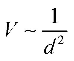
In the language of the complete tight-binding approximation for a heteronuclear tetrahedral semiconductor, U can be expressed as:39,41
Therefore, orbital overlap becomes weaker as the bond length increases. In monoelement crystals, bonding energy U is equal to V and can be expressed using only bond length d. Therefore, the cohesive energies were smaller for larger atomic radii. This also explained the interesting results mentioned earlier, where bandgaps became smaller with increasing bond length (atomic radius), such as in 2D group VA materials (Table S1, ESI†).
In a covalent crystal of AB, element A and B play equal roles in both the valence and conduction bands. As shown in Fig. 2b, the bandgap, Eg, is the energy difference between the bonding orbital and anti-bonding orbital, expressed as:39,41
Recent studies have reported that 2D group VA–VA materials are promising materials for optoelectronic and spin electronic applications.20–23,25,42 Following the above analysis, as group VA elements have the same valence electron configuration, but different atomic radii and electronegativities, their combination into group VA–VA monolayers is a good method for tuning their electronic properties for further possible interesting applications. We considered all possible 2D group VA–VA monolayers with buckled and puckered structures, as shown in Fig. S5 (ESI†). The optimized parameters and cohesive energies are summarized in Tables S5 and S6 (ESI†).
First, the stability of these 2D group VA–VA materials was examined. To address this, we calculated the cohesive energy of both group VA monolayers and VA–VA monolayers, which is a reasonable descriptor for the binding strength of connected frameworks.43 The cohesive energy is defined as Ecoh = (nEA + nEB − EAB)/2n, where EA, EB, and EAB are the total energies of a single A atom, a single B atom, and an AB monolayer, respectively. The calculated results (Tables S3 and S4, ESI†) showed that the α phase was more stable than the β phase for a 2D P monolayer, while the β phase was the most stable phase for As, Sb, and Bi. These results were consistent with previous studies, indicating the reliability of our cohesive calculation.4 Notably, the cohesive energy values of group VA–VA monolayers in the two phases were comparable to those of group VA monolayers, indicating strong bonding in the group VA–VA monolayer. Fig. 2c shows the more stable configurations of 2D group VA–VA monolayers between the two phases, providing useful information for experimental preparation.
The summarized results shown in Tables S5 and S6 (ESI†) also reveal an interesting trend between the lattice constant, bond parameter, and cohesive energy of 2D group VA–VA monolayers. When the bond length was larger, the bond angle and cohesive energy decreased, in accordance with the trend in group VA monolayers. Fig. S6 and S7 (ESI†) reflect the correlation between bond length (cohesive energy) and lattice parameter. Notably, the 2D puckered VA–VA monolayers showed only a good linear correlation between bond length or cohesive energy and lattice constant b (zigzag direction), but a disordered relationship along lattice constant a (armchair direction). This can be attributed to the degree of freedom for the lattice constants along different directions. More critical bond lengths and bond angles determined the extent of lattice constant a than that of lattice constant b.
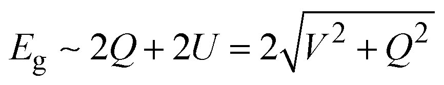
After exploring the stability of group VA–VA monolayers with fascinating bonding frameworks, we were curious about their electronic properties. First, we investigated the relationship between their bandgaps and the corresponding electronegativity and atomic radii, based on the aforementioned inference that the bandgap becomes wider with increasing electronegativity difference or orbital overlap. For 2D group VA monolayers, combination with a lighter group VA element simultaneously induced an electronegativity difference and larger orbital overlap, leading to a larger bandgap. However, combination with a heavier element produced a larger electronegativity difference and smaller orbital overlap, which competed to affect the bandgap value. The PBE functional described the correct band dispersion picture, but always underestimated the bandgap. To obtain more accurate bandgaps, we performed the HSE06 functional to describe the electronic structures. Unsurprisingly, the calculated bandgaps of group VA–VA monolayers reflected this inference well for both the α and β phase. The trends in bandgaps when combining with a lighter or heavier element are shown in Fig. 3a. When a group VA monolayer is combined with a lighter group VA element (for instance, bismuthene generally turns into BiSb → BiAs → BiP → BiN, antimonene turns into SbAs → SbP → SbN), the bandgaps increase steadily. However, when combined with a heavier element (such as P → PAs → PSb → PBi, As → AsSb → AsBi), the changes in bandgaps lacked regularity owing to the two competing factors. For example, NP in the puckered structure showed a smaller bandgap than NAs. The same irregularity was found in puckered P → PAs → PSb → PBi and As → AsSb → AsBi. However, for the 2D buckled structure, the bandgaps showed a continuous decline probably because electronegativity played a more important role than atomic radius in deciding the electronic structures.
 | ||
| Fig. 3 (a) Trends in bandgaps calculated by HSE06 functional when combining lighter or heavier elements in group VA monolayers. (b) Energy band alignments of 2D group VA–VA monolayers. | ||
The bandgap energies are essential for potential applications in electronics and optoelectronics. The 2D group VA–VA monolayers had wide-ranging bandgaps from 0.49 to 2.83 eV, corresponding to wavelengths ranging from infrared to visible light. As shown in Fig. 3b, we also provided energy band alignments, which provide important information for the construction of heterostructure-based next-generation electronic and optoelectronic devices. For example, buckled PBi and AsSb with close lattice constants were well suited to building both lateral and vertical heterostructures. Furthermore, puckered AsSb, AsBi, and SbBi with small bandgaps were candidates for forming type-I heterostructures with wide-bandgap materials. Puckered PSb, PBi, AsSb, AsBi, and SbBi with a high valence band maximum (VBM) of up to −4 eV were well suited to type-II heterostructures. Buckled NP, NAs, NSb, and NBi with a low conduction band minimum (CBM) can be combined with high-VBM materials to form type-II or III heterostructures.
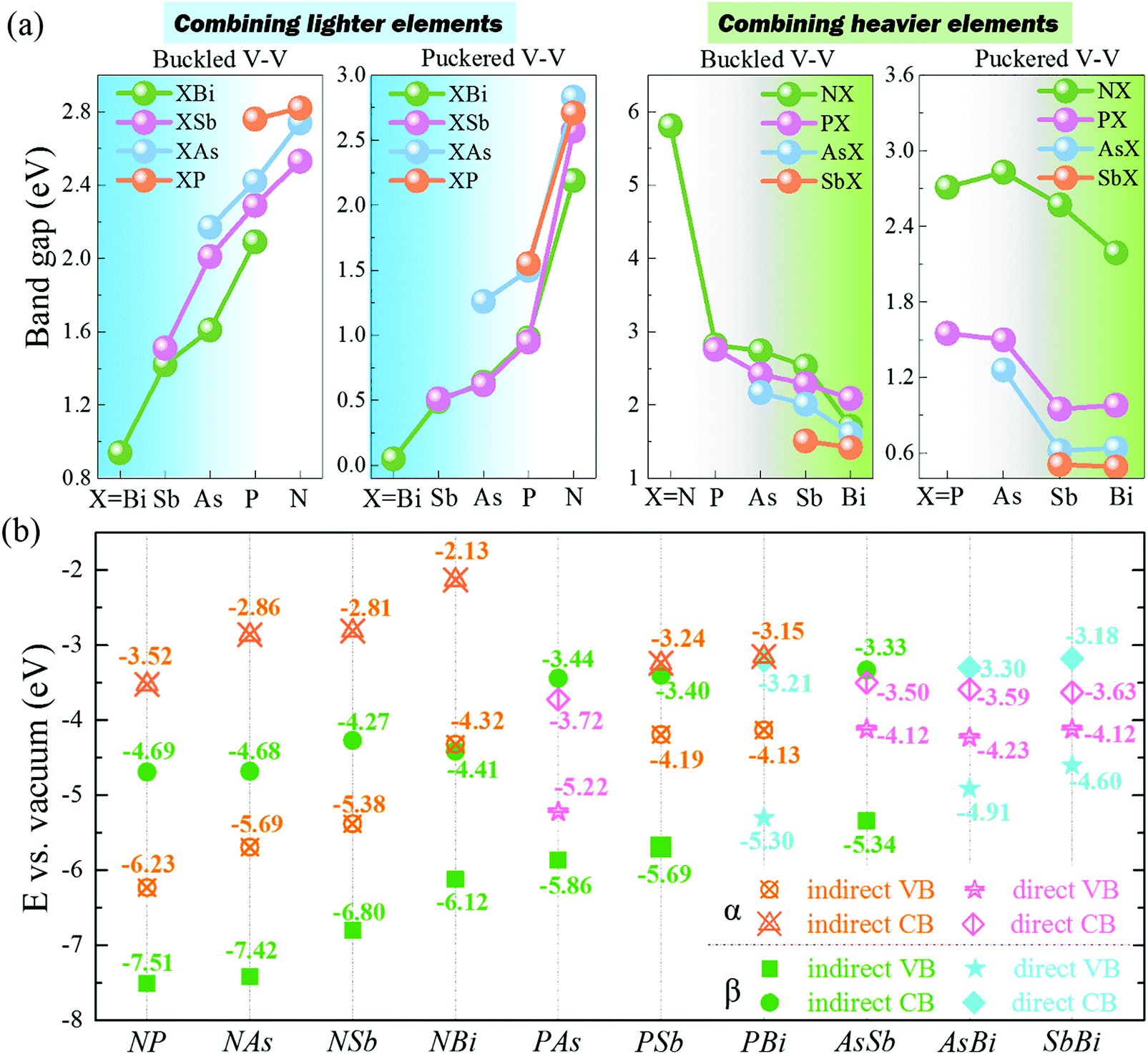
Remarkably, after chemical combination, more direct bandgap semiconductors emerged among these group VA–VA monolayers, providing more opportunities for nanoelectronic and optoelectronic applications. To investigate the change from indirect bandgap to direct bandgap after combination, we selected β-P/β-PBi, and α-As/α-AsBi as examples to explore the orbital-resolved band structures of group VA–VA monolayers before and after combination, as shown in Fig. 4. The 2D group VA–VA monolayers exhibited covalent characteristics that both different VA elements contributed to equally in both the valence and conduction bands. Consequently, we found an orbital-resolved band structure instead of an atomic-resolved band structure. The physical pictures of their band structures were similar, despite the combination with other group VA elements. However, such a small change resulted in ideal electronic properties. For buckled P and puckered As, the indirect bandgap transformed into a direct bandgap by combining with Bi. From β-P to β-PBi, points 1 and 2 were always occupied by pz and pxy orbitals, respectively. In PBi, points 1 and 2 were mainly donated by P, leading to the valence band maximum (VBM) exchanging from point 1 to point 2. A strong orbital splitting occurred in the conduction band. Point 4 dropped to become the CBM instead of point 3. We then turned our attention to α-As and its composite AsBi. Point 4 was occupied by s and pxy orbitals in As. However, in AsBi, point 4 was mainly occupied by a pxy orbital. The CBM transformed from point 3 to 4 after combining with Bi. Furthermore, valence band states had more lighter-element character, while conduction band states had heavier-element character, subject to their electronegative differences.
 | ||
| Fig. 4 Orbital-resolved band structures and the corresponding charge density of valence and conduction bands in (a) β-P, (b) β-PBi, (c) α-As, and (d) α-AsBi. Red represents s orbital contribution; blue represents pxy contribution; green represents pz contribution. Isosurface value was set to (a and b) 0.012 e Bohr−3 and (c and d) 0.007 e Bohr−3. Band structures were calculated using the HSE06 functional. | ||
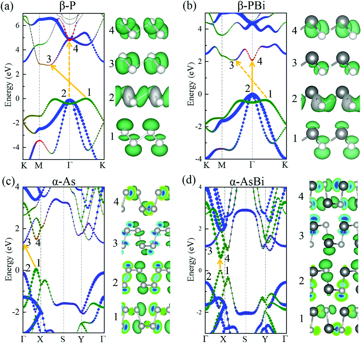
Interestingly, 2D buckled NX (X = P, As, Sb, Bi) showed Mexican-hat band edges at the valence band near the Fermi level, as shown in Fig. 5a. The three-dimensional Mexican-hat band dispersion is clearly shown in Fig. 5b. In addition to buckled NX, other 2D buckled VA–VA monolayers had another band dispersion exceeding the Mexican-hat valley near the Fermi level at a Γ high-symmetry point. The Mexican-hat band dispersion in the 2D buckled VA–VA monolayers resulted in a high density of states (DOS) near the Fermi level and a Van Hove singularity. The strong singularity in the DOS near the Fermi level was highly important. A high charge density near the Fermi level can cause electronic instability, which often results in magnetism and superconductivity.44,45
 | ||
| Fig. 5 (a and b) Schematic diagram of band dispersion near the VBM of β-XBi monolayer. (c and d) Band dispersion near the CBM of β-XBi (c) without and (d) with SOC. | ||
To account for the heavy elements (Sb and Bi) in group VA–VA monolayers, the SOC effect was included in band structure calculations. The band structures with SOC effect are shown in Fig. S9 and S10 (ESI†). The bandgaps decreased significantly when heavy elements were present. Our calculated results showed that the SOC effect on the band structures of 2D buckled PBi, AsSb, AsBi, and SbBi monolayers was considerable, leading to the disappearance of their Mexican-hat band edges. Remarkably, for 2D buckled PBi, AsBi, and SbBi monolayers, the SOC effect induced giant Rashba spin splitting in the conduction band of 2D buckled XBi (X = N, P, As, Sb), as shown in Fig. 5c and d. Notably, the buckled Bi monolayer had a Rashba splitting in the valence band after applying the SOC effect. We quantitatively described the strength of their Rashba spin splitting using the Rashba energy, ER, Rashba momentum, k0, and Rashba parameter, αR, as summarized in Table S7 (ESI†).46 Rashba parameter αR is defined by αR = 2ER/k0. The Rashba splitting strength of 2D buckled XBi monolayers was comparable with that of some bulk Rashba semiconductors.47–49 Owing to their nanoscale thickness and suitable bandgap, 2D buckled XBi monolayers are expected to be candidate materials for spin field-effect transistors and optoelectronic devices.
Conclusion
In summary, we performed the chemical combination of group VA elements to realize the band engineering of 2D group VA materials. These 2D bi-element materials with buckled and puckered structures are named 2D group VA–VA materials. The atomic radii and electronegativities greatly influenced their geometric structures and electronic properties. We compared the cohesive energies of 2D group VA–VA materials with those of 2D group VA materials to confirm the similar bond strengths in their atomic structures. The bandgaps of 2D group VA–VA materials were related to their atomic radii and electronegativities. We also provided the energy levels of the 2D group VA–VA materials, which are essential for the construction of heterostructures. Particularly, in the band dispersion of 2D buckled NX and XBi, Mexican-hat dispersion and Rashba spin splitting were observed in the valence and conduction bands, respectively. We expect this theoretical study to promote the further experimental realization of 2D group VA–VA materials, improving their potential for nanoelectronic and optoelectronic applications.Conflicts of interest
There are no conflicts of interest to declare.Acknowledgements
This work was financially supported by the National Natural Science Foundation of China (Grant No. 61704082) and Natural Science Foundation of Jiangsu Province (BK20170851, BK20180071).References
- C. Tan, X. Cao, X. J. Wu, Q. He, J. Yang, X. Zhang, J. Chen, W. Zhao, S. Han, G. H. Nam, M. Sindoro and H. Zhang, Chem. Rev., 2017, 117, 6225–6331 CrossRef CAS PubMed.
- X. Kong, Q. Liu, C. Zhang, Z. Peng and Q. Chen, Chem. Soc. Rev., 2017, 46, 2127–2157 RSC.
- P. Miro, M. Audiffred and T. Heine, Chem. Soc. Rev., 2014, 43, 6537–6554 RSC.
- S. Zhang, S. Guo, Z. Chen, Y. Wang, H. Gao, J. Gomez-Herrero, P. Ares, F. Zamora, Z. Zhu and H. Zeng, Chem. Soc. Rev., 2018, 47, 982–1021 RSC.
- Y. Guo, L. Ma, K. Mao, M. Ju, Y. Bai, J. Zhao and X. C. Zeng, Nanoscale Horiz., 2019, 4, 592–600 RSC.
- Y. Guo, Q. Wu, Y. Li, N. Lu, K. Mao, Y. Bai, J. Zhao, J. Wang and X. C. Zeng, Nanoscale Horiz., 2019, 4, 223–230 RSC.
- Z. Jiang, P. Wang, X. Jiang and J. Zhao, Nanoscale Horiz., 2018, 3, 335–341 RSC.
- A. Ambrosi, C. K. Chua, N. M. Latiff, A. H. Loo, C. H. Wong, A. Y. Eng, A. Bonanni and M. Pumera, Chem. Soc. Rev., 2016, 45, 2458–2493 RSC.
- K. S. Novoselov, A. K. Geim, S. V. Morozov, D. Jiang, Y. Zhang, S. V. Dubonos, I. V. Grigorieva and A. A. Firsov, Science, 2004, 306, 666–669 CrossRef CAS PubMed.
- L. Peng, Y. Cui, L. Sun, J. Du, S. Wang, S. Zhang and Y. Huang, Nanoscale Horiz., 2019, 4, 480–489 RSC.
- S. Balendhran, S. Walia, H. Nili, S. Sriram and M. Bhaskaran, Small, 2015, 11, 640–652 CrossRef CAS PubMed.
- L. K. Li, Y. J. Yu, G. J. Ye, Q. Q. Ge, X. D. Ou, H. Wu, D. L. Feng, X. H. Chen and Y. B. Zhang, Nat. Nanotechnol., 2014, 9, 372–377 CrossRef CAS PubMed.
- H. Liu, A. T. Neal, Z. Zhu, X. Xu, D. Tomanek, P. D. Ye and Z. Luo, ACS Nano, 2014, 8, 4033–4041 CrossRef CAS PubMed.
- S. Zhang, Z. Yan, Y. Li, Z. Chen and H. Zeng, Angew. Chem., Int. Ed., 2015, 54, 3112–3115 CrossRef CAS PubMed.
- S. Zhang, M. Xie, F. Li, Z. Yan, Y. Li, E. Kan, W. Liu, Z. Chen and H. Zeng, Angew. Chem., Int. Ed., 2016, 128, 1698–1701 CrossRef.
- J. P. Ji, X. F. Song, J. Z. Liu, Z. Yan, C. X. Huo, S. L. Zhang, M. Su, L. Liao, W. H. Wang, Z. H. Ni, Y. F. Hao and H. B. Zeng, Nat. Commun., 2016, 7, 13352 CrossRef CAS PubMed.
- F. Reis, G. Li, L. Dudy, M. Bauernfeind, S. Glass, W. Hanke, R. Thomale, J. Schäfer and R. Claessen, Science, 2017, 357, 287–290 CrossRef CAS PubMed.
- S. L. Zhang, W. H. Zhou, Y. D. Ma, J. P. Ji, B. Cai, S. A. Yang, Z. Zhu, Z. F. Chen and H. B. Zeng, Nano Lett., 2017, 17, 3434–3440 CrossRef CAS PubMed.
- G. X. Wang, R. Pandey and S. P. Karna, ACS Appl. Mater. Interfaces, 2015, 7, 11490 CrossRef CAS PubMed.
- M. Long, A. Gao, P. Wang, H. Xia, C. Ott, C. Pan, Y. Fu, E. Liu, X. Chen, W. Lu, T. Nilges, J. Xu, X. Wang, W. Hu and F. Miao, Sci. Adv., 2017, 3, e1700589 CrossRef PubMed.
- M. Amani, E. Regan, J. Bullock, G. H. Ahn and A. Javey, ACS Nano, 2017, 11, 11724–11731 CrossRef CAS PubMed.
- B. Liu, M. Kopf, A. N. Abbas, X. Wang, Q. Guo, Y. Jia, F. Xia, R. Weihrich, F. Bachhuber, F. Pielnhofer, H. Wang, R. Dhall, S. B. Cronin, M. Ge, X. Fang, T. Nilges and C. Zhou, Adv. Mater., 2015, 27, 4423–4429 CrossRef CAS PubMed.
- S. Yuan, C. Shen, B. Deng, X. Chen, Q. Guo, Y. Ma, A. Abbas, B. Liu, R. Haiges, C. Ott, T. Nilges, K. Watanabe, T. Taniguchi, O. Sinai, D. Naveh, C. Zhou and F. Xia, Nano Lett., 2018, 18, 3172–3179 CrossRef CAS PubMed.
- H. Gao, J. Niu, C. Zhang, Z. Peng and Z. Zhang, ACS Nano, 2018, 12, 3568–3577 CrossRef CAS PubMed.
- N. H. D. Khang, Y. Ueda and P. N. Hai, Nat. Mater., 2018, 17, 808–813 CrossRef CAS PubMed.
- B. Cai, M. Xie, S. Zhang, C. Huang, E. Kan, X. Chen, Y. Gu and H. Zeng, Sci. China Mater., 2016, 59, 648–656 CrossRef CAS.
- Z. Liu, W. Feng, H. Xin, Y. Gao, P. Liu, Y. Yao, H. Weng and J. Zhao, Mater. Horiz., 2019, 6, 781–787 RSC.
- G. Kresse and D. Joubert, Phys. Rev. B: Condens. Matter Mater. Phys., 1999, 59, 1758 CrossRef CAS.
- P. E. Blöchl, Phys. Rev. B: Condens. Matter Mater. Phys., 1994, 50, 17953 CrossRef.
- J. P. Perdew, K. Burke and M. Ernzerhof, Phys. Rev. Lett., 1996, 77, 3865 CrossRef CAS PubMed.
- J. Heyd, G. E. Scuseria and M. Ernzerhof, J. Chem. Phys., 2006, 124, 219906 CrossRef.
- H. J. Monkhorst and J. D. Pack, Phys. Rev. B: Condens. Matter Mater. Phys., 1976, 13, 5188 CrossRef.
- B. Delley, J. Chem. Phys., 2000, 113, 7756–7764 CrossRef CAS.
- B. Delley, J. Chem. Phys., 1990, 92, 508–517 CrossRef CAS.
- A. D. Deepthi Jose, Acc. Chem. Res., 2014, 47, 593–602 CrossRef.
- H. Şahin, S. Cahangirov, M. Topsakal, E. Bekaroglu, E. Akturk, R. T. Senger and S. Ciraci, Phys. Rev. B: Condens. Matter Mater. Phys., 2009, 80, 155453 CrossRef.
- I. B. Bersuker, Chem. Rev., 2013, 113, 1351–1390 CrossRef CAS PubMed.
- H. L. Zhuang, A. K. Singh and R. G. Hennig, Phys. Rev. B: Condens. Matter Mater. Phys., 2013, 87, 165415 CrossRef.
- G. S. Rohrer, Structure and bonding in crystalline materials, Cambridge University Press, 2001 Search PubMed.
- T. Koopmans, Physica, 1934, 1, 104–113 CrossRef.
- W. A. Harrison, Electronic Structure and the Properties of Solids: the Physics of the Chemical Bond, Courier Corporation, 2012 Search PubMed.
- Z. Zhu and D. Tomanek, Phys. Rev. Lett., 2014, 112, 176802 CrossRef PubMed.
- Y. Wang, M. Qiao, Y. Li and Z. Chen, Nanoscale Horiz., 2018, 3, 327–334 RSC.
- Y. Nie, M. Rahman, P. Liu, A. Sidike, Q. Xia and G. Guo, Phys. Rev. B: Condens. Matter Mater. Phys., 2017, 96, 075401 CrossRef.
- H. Sevinçli, Nano Lett., 2017, 17, 2589–2595 CrossRef PubMed.
- D. D. Sante, P. Barone, R. Bertacco and S. Picozzi, Adv. Mater., 2013, 25, 509–513 CrossRef.
- L. G. D. da Silveira, P. Barone and S. Picozzi, Phys. Rev. B: Condens. Matter Mater. Phys., 2016, 93, 245159 CrossRef.
- A. Narayan, Phys. Rev. B: Condens. Matter Mater. Phys., 2015, 92, 220101 CrossRef.
- F. X. Xiang, X. L. Wang, M. Veldhorst, S. X. Dou and M. S. Fuhrer, Phys. Rev. B: Condens. Matter Mater. Phys., 2015, 92, 035123 CrossRef.
Footnote |
| † Electronic supplementary information (ESI) available. See DOI: 10.1039/c9nh00215d |
| This journal is © The Royal Society of Chemistry 2019 |