
Monitoring the morphological evolution in mixed-dimensional lead bromide perovskite films with lamellar-stacked perovskite nanoplatelets†
Rui
Wang
 ab,
Yu
Tong
cd,
Kun
Wang
b,
Senlin
Xia
b,
Emmanuel
Kentzinger
e,
Olaf
Soltwedel
fg,
Peter
Müller-Buschbaum
*bh and
Henrich
Frielinghaus
*a
ab,
Yu
Tong
cd,
Kun
Wang
b,
Senlin
Xia
b,
Emmanuel
Kentzinger
e,
Olaf
Soltwedel
fg,
Peter
Müller-Buschbaum
*bh and
Henrich
Frielinghaus
*a
aJülich Centre for Neutron Science (JCNS) at Heinz Maier-Leibnitz Zentrum (MLZ), Forschungszentrum Jülich GmbH, Lichtenbergstr. 1, 85748 Garching, Germany. E-mail: h.frielinghaus@fz-juelich.de
bPhysik-Department, Lehrstuhl für Funktionelle Materialien, Technische Universität München, James-Franck-Str. 1, 85748 Garching, Germany. E-mail: muellerb@ph.tum.de
cChair for Photonics and Optoelectronics, Nano-Institute Munich, Department of Physics, Ludwig-Maximilians-Universität (LMU), Königinstr. 10, 80539 Munich, Germany
dNanosystems Initiative Munich (NIM) and Center for NanoScience (CeNS), Schellingstr. 4, 80799 Munich, Germany
eJülich Centre for Neutron Science JCNS, Peter Grünberg Institut PGI, JARA-FIT, Forschungszentrum Jülich GmbH, 52425 Jülich, Germany
fPhysik-Department, Lehrstuhl für Topologie korrelierte Elektronensysteme, Technische Universität München, James-Franck-Str. 1, 85747, München, Germany
gPhysik-Department, Lehrstuhl für Weiche Materie an Grenzflächen, Technische Universität Darmstadt, 64287, Darmstadt, Germany
hHeinz Maier-Leibnitz Zentrum (MLZ), Technische Universität München, Lichtenbergstr. 1, 85748 Garching, Germany
First published on 23rd April 2019
Abstract
Mixed-dimensional lead bromide perovskite films combine the properties of both three-dimensional (3D) and two-dimensional (2D) perovskite crystals, and due to their good humidity tolerance, they emerge as promising candidates for long-term stable optoelectronic applications. In order to further tailor the film morphology aiming for a better device performance, it is important to unravel the structural formation mechanism in these perovskite thin films. In the present study, the formation of 3D lead bromide perovskite crystals and the self-assembly of lamellar-stacked 2D perovskite nanoplatelets are comprehensively studied. Samples are prepared through a two-step vapor assisted route with different vapor exposure times in order to monitor the detailed morphology at the specific reaction stage. With grazing incidence X-ray scattering techniques, the preferential orientation of the 3D crystals is found to decrease upon increasing the reaction time. Also, it is evidenced that well-ordered in-plane lamellar-stacked 2D nanoplatelets form aggregates in the bulk structure only. The obtained hierarchical morphology shows excellent structural stability in a humid atmosphere even at a relative humidity level of 80%. Our findings statistically offer a morphological understanding, which is important for the optimization of the sample preparation route and thus the resulting performance of moisture-tolerant perovskite based optoelectronic devices.
New conceptsLead halide perovskites have attracted tremendous research attention for optoelectronic applications due to their outstanding dielectric properties. In order to enhance the stability of lead halide perovskites in a humid atmosphere, a promising approach is to use mixed-dimensional perovskites (MDPs) (a combination of both quasi-2D and 3D perovskites) as photoactive materials. The present study gives new conceptual insights into the formation of 3D lead bromide perovskite crystals and the self-assembly of lamellar-stacked 2D perovskite nanoplatelets investigated by grazing incidence X-ray scattering techniques. We observe that the preferential orientation of the 3D crystals decreases upon increasing the reaction time and that well-ordered in-plane lamellar-stacked 2D nanoplatelets form aggregates and only build in the sample volume. An excellent structural stability in a humid atmosphere even at a relative humidity level of 80% is achieved. The presented morphological understanding is important for future application of perovskites in optoelectronic devices. |
Introduction
Lead halide perovskites have attracted tremendous research attention for optoelectronic applications due to their outstanding dielectric properties. However, several challenges reported so far, such as their limited long-term stability and their voltage–current hysteresis,1–4 prevent their commercialization. In order to enhance the stability of lead halide perovskites in a humid atmosphere, different approaches have been explored to elevate the threshold of degradation including the use of two-dimensional (2D) Ruddlesden–Popper perovskites instead of their neat three-dimensional (3D) counterparts or directly utilize mixed-dimensional perovskites (MDPs) (a combination of both quasi-2D and 3D perovskites) as photoactive materials.5–8For example, Wang et al. used n-butylammonium to prepare 2D/3D heterostructured lead halide perovskite films and found that the inclusion of n-butylammonium effectively improved the thin film crystallinity. By reducing the number of defects at grain boundaries, the long-term solar cell stability was improved.9 Lee et al. reported that by incorporating a small fraction of a 2D perovskite into a conventional 3D perovskite precursor, the 2D perovskite spontaneously forms humidity-resistant layers at the 3D perovskite grain boundaries.10 From contact angle measurements, it was observed that the addition of the bulky organic ligand passivated the thin film surface and subsequently improved its moisture tolerance.11–13 However, a comprehensive understanding of the mechanism preventing the penetration of the water molecules into the film volume is still limited.
More interestingly, by tailoring their dimensionality, 2D perovskites, which exhibit quantum confinement, can cause inherent interaction between 2D and 3D perovskites in the MDP film and generate new phenomena.14 Concentrated charge carriers due to energy funnelling were reported in multilayered quasi-2D perovskite films, which consequently affected the radiative recombination efficiency and improved the performance of light-emitting diodes.15,16 In our previous study we reported that the energy transfer in MDP films is closely correlated with the thin film morphology.17 Therefore, gaining detailed morphological insight into the structure formation of MDP films is important.
Results and discussion
In the present study, mixed dimensional perovskite films are fabricated through a two-step vapor assisted deposition process.18 As illustrated in Fig. 1a, the spin-coated lead bromide (PbBr2) films are in situ reacted with an organic vapor composed of methylammonium bromide (MABr) and octylammonium bromide (OABr) for different exposure times. The obtained samples are named S5 (5 min vapor exposure), S30 (30 min), S60 (60 min), and S120 (120 min). This two-step evaporation route avoids fast kinetics, due to the ionic nature of the metathesis reaction,19 and thus allows for better synthetic control at the specific reaction stage. During the sample preparation, the color of the perovskite film gradually transforms to yellowish, indicating the formation of the lead bromide perovskite.14 This is further demonstrated using the UV-vis spectra (Fig. 1b). A discernible shoulder at 520 nm is visible for sample S5, which is close to the absorption onset of a 3D bulk-like MAPbBr3 perovskite.20 Upon further increasing the exposure time, the absorption edge becomes steep for samples S30 and S60, whereas for the sample with the longest reaction time (120 min), it clearly blue-shifts to 511 nm, likely due to the quantum confinement effect.21 In addition, three features at 472 nm, 451 nm and 433 nm become more prominent for longer exposure times, which can be attributed to the formation of 2D perovskite nanoplatelets (OA)2(MA)nPbn+1Br3n+4, with perovskite unit cell thicknesses (n) of 4, 3, and 1, respectively.22,23 A closer inspection of the photoluminescence (PL) spectra reveals similar results (Fig. 1c). The main emission peak first shifts toward the PL position of the 3D MAPbBr3 perovskite (533 nm) for samples prepared until a reaction time of 60 min (S60). Afterwards, it is 44 meV blue-shifted to 523 nm for sample S120 (Fig. 1c), close to the values reported for quasi-2D lead bromide perovskites with n = 7–10.21,24 In contrast, the PL peaks of the aforementioned perovskite nanoplatelets continuously blue shift to shorter wavelengths indicating even stronger quantum confined. The presence of long chain organic ligand OABr on the surfaces of the perovskite crystals will vary the crystallization rate.25 This anisotropic optical observation between 3D bulk-like and 2D perovskite nanoplatelets implies that the structure formation rates are different for 2D and 3D perovskite crystals.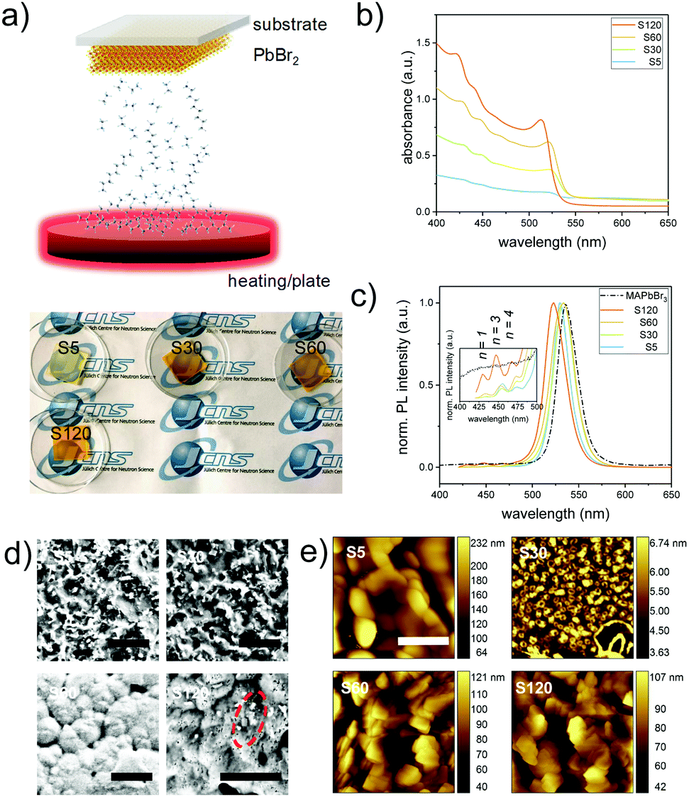 | ||
| Fig. 1 (a) Schematic illustration of the vapor-assisted perovskite film synthesis process and photographs of the resulting perovskite films on quartz substrates after different exposure times. (b) UV-vis absorption and (c) PL-spectra of the MDP films. The peak positions for perovskite nanoplatelets are indexed in the PL-spectra. (d) SEM (scale bar 1 μm) and (e) AFM (scale bar 400 nm) surface morphologies for MDP films prepared with 5 min (S5), 30 min (S30), 60 min (S60) and 120 min (S120) vapor exposure times. Example of perovskite nanoplatelets is highlighted by a red dashed circle in the SEM image. | ||
To determine the surface morphology, the obtained films are studied by scanning electron microscopy (SEM) and atomic force microscopy (AFM). As shown in Fig. 1d and e, respectively, the surface structures of the obtained films vary as a function of the exposure time to the organic vapor. On the local morphology as determined with SEM on a micrometer scale (Fig. 1d), a very rough surface with individual rectangular like crystals (∼0.1 μm size) is produced at the beginning of the reaction stage (S5 and S30). Increasing the exposure time to 60 min (S60) induces the growth of large grains (typically over 0.5 μm), which are densely packed. For sample S120, the surface compactness further increases, and a small number of randomly distributed platelet-like structures are observed. The increase of domain sizes along the in-plane direction with increasing exposure time is speculated to originate from an Ostwald ripening process, which is typical in perovskite crystal growth.26,27 It is well known that lead halide perovskites suffer from morphological degradation under electron beam irradiation.28 Therefore, AFM is employed as well to determine the local surface morphology on a nanometer scale. Round-shaped crystals (∼200 nm) are seen in the case of sample S5. Upon increasing the reaction time to 30 min, the domain size dramatically decreases to ∼60 nm, which is likely due to the conversion of PbBr2 to perovskite crystals. For samples with an exposure time above 60 min, the film surface morphology is dominated by platelet-like structures (Fig. S1, ESI†), indicating that an increased amount of low-dimensional perovskite crystals has formed for longer reaction times. More specifically, these platelet-like crystals are randomly oriented on the surfaces and no distinct stack-order can be observed via AFM.
The crystalline structures of the four MDP films as well as of a pre-deposited PbBr2 film were studied using grazing incidence wide angle X-ray scattering (GIWAXS). The obtained 2D GIWAXS patterns remarkably develop with varying exposure time. In Fig. 2a, the neat PbBr2 film crystallized with a preferential orientation with respect to the substrate surface as evidenced by the strong intensity of the (002) Bragg peak along the qz direction (Fig. 2a and g). Upon exposure of the PbBr2 film to the organic vapor for 5 min, the diffraction pattern of MAPbBr3 starts to arise for 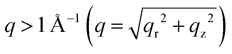 , implying that the 3D MAPbBr3 perovskite crystals are already formed within the shortest chosen reaction time. Simultaneously, another three distinct scattering features are revealed for q < 1 Å−1. These features are in line with earlier findings and can be assigned to the ordered precursor phase during perovskite crystal formation.29 The (002) Bragg peak intensity of PbBr2 vanishes upon increasing the exposure time (Fig. 2f), whereas the diffraction pattern of MAPbBr3 continues to evolve. In sample S30, both PbBr2 and perovskite phases can be identified, thus explaining the unique surface morphology in Fig. 1e originating from the perovskite crystal formation. A careful examination of the (001) Bragg peak reveals a slight shift of the peak position from 1.056 to 1.062 Å−1 for longer exposure times (Fig. S2, ESI†), being indicative of a decreased d-spacing from 5.95 to 5.92 Å. This observation can be explained by the constrained crystallization of quasi-2D perovskite crystals in comparison to 3D bulk-like perovskite crystals.30 Thus, the film transformed into a quasi-2D like system in sample S120. This observation is in good accordance with the PL result that the main emission in sample S120 is a characteristic of quasi-2D perovskites with unit cell thicknesses n = 7–10 (Fig. 1c). A further discussion of this compositional evolution is provided later. In Fig. 2b, a segregated azimuthal intensity profile of the (001) Bragg peak with apparent intensity distribution along the qz direction is seen in the 2D GIWAXS data for sample S5, indicating that the MAPbBr3 crystals tend to adopt a face-on orientation, with the (001) planes being parallel to the substrate. To further study the evolution of the MAPbBr3 crystal orientation, azimuthal integrations of the (001) Bragg peaks are done for the four MDP films (Fig. S3, ESI†). In Fig. S3a (ESI†), an extended range of the azimuthal angle of the oriented crystals is readable for longer exposure times and indicates a crystal reorientation during the perovskite conversion (Fig. 2g). A detailed inspection of the orientation profile reveals that the preferential orientation decreases from 61.3% in sample S5 to 54.5% in sample S120. This crystal reorientation process is speculated to be energetically favorable when the OABr ligand slices the 3D perovskite crystal to form a quasi-2D system. For q < 1 Å−1, the scattering signals become more intense for longer exposure times due to the formation of low dimensional perovskite nanoplatelets.18,21 Since the scattering details for perovskite nanoplatelet aggregates are located for smaller q values, they cannot be accessed with GIWAXS, and the samples are further studied with higher q-resolution using grazing incidence small angle X-ray scattering (GISAXS).
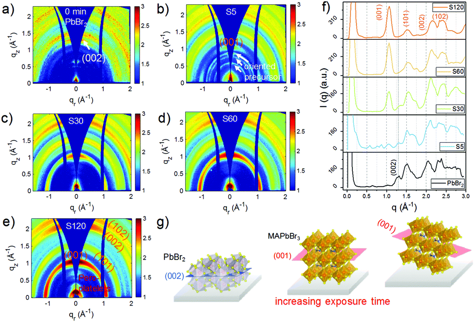 | ||
| Fig. 2 2D GIWAXS data of (a) lead bromide (PbBr2) and MDP films prepared with (b) 5 min (S5), (c) 30 min (S30), (d) 60 min (S60) and (e) 120 min (S120) exposure times. (f) Integrated intensity profiles of GIWAXS data. The vanishing of the PbBr2(002) Bragg peak upon increasing the exposure time is indicated with a black dashed line. (g) Schematic illustration of the crystal formation evolution during perovskite conversion. | ||
Fig. 3 displays the 2D GISAXS data of the PbBr2 film and the four MDP films with different vapor exposure times. The positions for the specular peak and the Yoneda peak are highlighted in Fig. 3a. The Yoneda peak is a sample characteristic feature which is closely correlated with the specific material composition.31,32 In Fig. S4 (ESI†), a detailed inspection around the Yoneda peak position once again demonstrates that the MDP film becomes more quasi-2D like for the longer exposure times. After exposing the PbBr2 film to the organic vapor for 5 min, a broad shoulder-like scattering contribution at ∼2.51 nm−1 and a sharp peak at ∼5.68 nm−1 are seen. In comparison to the 2D GISAXS data of PbBr2 (Fig. 3a), the origin of the latter peak can be related to the increased distance between the lead layers after the MA cation incorporation. Upon increasing the vapor exposure time, the shoulder-like scattering feature shifts to a smaller q value of ∼1.98 nm−1, corresponding to a spacing distance of 3.2 nm. Using the MAPbBr3 unit cell thickness ∼0.59 nm and the length of the OA ligand ∼1 nm, this characteristic length approximately matches the thickness of perovskite nanoplatelets with unit cell thickness n = 3. The Bragg peak becomes both intense and sharp with increasing vapor exposure time. As shown in Fig. 3g, the full width at half maximum (FWHM) of the Bragg peak distinctively decreases after 60 min. Accordingly, these nanoplatelets exhibit better ordering for the longer exposure time. For sample S120 (Fig. 3e), the second order of the Bragg peak is found along the surface normal (qz), which evidences that the perovskite nanoplatelets form a lamellar-stacked superlattice. More specifically, these superlattice structures have a preferential orientation parallel to the substrate surface (Fig. S5, ESI†). In addition, another feature evolves with increasing vapor exposure time. In Fig. 3f, a peak at ∼2.3 nm−1 arises for samples S60 and S120. This indicates the formation of 2D nanoplatelets with unit cell thickness n = 2.17 To determine the in-plane (qy) nanostructures for different exposure times, horizontal line cuts of the 2D GISAXS data are made at the Yoneda peak position of the perovskite nanoplatelets with a unit cell thickness n = 3. The obtained results are plotted in the Kratky plots in Fig. 3h. It is found that apart from the better lamellar symmetry along the substrate surface normal, ordered in-plane structures formed for longer exposure times. A broad peak is seen at ∼0.22 nm−1, implying an in-plane distance of ∼28.2 nm between the neighbouring superlattice domains. Since no such structures are found by SEM and AFM (Fig. 1e and f), the ordered lamellar stacked superlattice domains are expected to self-assemble inside the film volume and not on the film surface. A schematic illustration for the superlattice domains is depicted in Fig. 3i. In Fig. 2b, 3D MAPbBr3 perovskite crystals are already formed in the case of the sample with the shortest vapor exposure time (S5). Considering the bulky length of the OABr ligands, we speculate that the slower formation of the 2D nanoplatelets is due to the low mobility of the longer organic ligands. The 2D nanoplatelets first form on the surface of the MDP film. After longer reaction times, a larger amount of OABr molecules penetrates deeper into the film volume and leads to the formation of ordered lamellar-stacked aggregates. This is different from what we observed before in solution processed films, in which the bulky organic ligand functionalized as a morphological template that tuned the crystal orientation.17
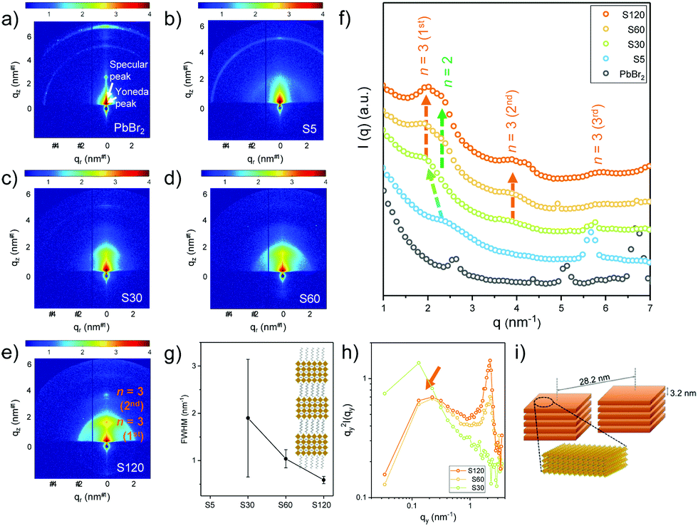 | ||
| Fig. 3 2D GISAXS data of (a) lead bromide (PbBr2) and MDP films prepared with (b) 5 min (S5), (c) 30 min (S30), (d) 60 min (S60) and (e) 120 min (S120) exposure times. (f) Integrated intensity profiles of the GISAXS data. The shifts of the nanoplatelets’ peaks are highlighted with colored arrows. (g) Evolution of FWHM for perovskite nanoplatelets’ peaks for different exposure times. A schematic illustration of a lamellar-stacked perovskite superlattice with a unit cell thickness n = 3 is shown in the inset. (h) Horizontal line cuts of the 2D GISAXS data taken at the Yoneda peak positions of perovskite nanoplatelets with unit cell thickness n = 3 for samples S30, S60 and S120. (i) A schematic illustration of the lamellar-stacked perovskite superlattice with a unit cell thickness n = 3. | ||
To further examine the structural stability of the obtained MDP films in a humid atmosphere, in situ X-ray reflectivity (XRR) measurements are carried out for sample S120 at different relative humidity (RH) levels. The sample is put in a closed humidity chamber at a constant temperature of ∼23 °C and a feedback-controlled mixture of dry and water saturated nitrogen is used to generate precise and stable humidity around the sample position. Before the acquisition of the XRR data, the sample is equilibrated at each RH level for 1 h. As shown in Fig. 4a, the Bragg peaks of the 2D perovskite nanoplatelets, the bulk-like perovskite crystals and the crystallized OA ligands are well resolved in the obtained XRR data. In addition, the Bragg peak of the OA ligands for sample S120 has the highest intensities among the four MDP films, which indicates that the bulky ligand is well ordered and therefore contributes to the formation of the lamellar-stacked aggregate (Fig. S6, ESI†).17 The peak intensities are very stable until the RH level reaches 80% (Fig. 4b), indicating that the surface adopted OABr ligands contribute a good water resistance to the MDP crystals. Upon further increasing the RH level to 100%, the reflection peak of the OABr ligand at ∼0.7 Å−1 collapses, and therefore the surface passivation effect diminishes, leading to the disappearance of the Bragg peaks of both the perovskite nanoplatelets and the bulk-like perovskite crystals. However, it is noted that the higher orders of the Bragg peak that represent the lamellar-stacked nanoplatelet aggregates with n = 3 unit cell thickness are still observable at a humidity level of 100%. This observation implies that the surface distributed nanoplatelets act as a barrier preventing water molecules from penetrating into the film volume (Fig. 4c). As a consequence, the overall structural stability is improved.
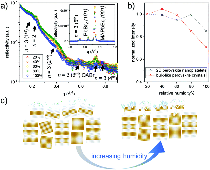 | ||
| Fig. 4 (a) XRR data of sample S120 at different relative humidity (RH) levels as indicated. The obtained Bragg peaks for a larger q range is shown as inset. (b) Normalized peak intensities of the first order Bragg peak of the 2D nanoplatelets (n = 3) and the (001) Bragg peak of the bulk-like MAPbBr3 crystal. (c) Schematic illustration of the structural evolution of the MDP film upon increasing the RH level. | ||
Conclusions
In summary, the morphological evolution of MDP films during vapor-assisted sample preparation is comprehensively studied. 3D bulk perovskite crystals form more rapidly in comparison with 2D perovskite nanoplatelets and adopt a preferential crystal orientation with respect to the substrate surface. In the initial stage, 2D nanoplatelets form on the film surface and lack long-range ordering. After longer reaction times, lamellar-stacked superlattices start to evolve and form aggregates in the film volume with a correlation distance of around 28 nm. In situ XRR measurements reveal that due to the passivation effect of the OABr ligands and the surface distributed 2D nanoplatelets, the obtained MDP films show excellent water inertness until a RH level of 80%. Upon further increasing the RH level to 100%, this passivation layer collapses but still protects the lamellar-stacked superlattice in the bulk. The obtained insights offer a fundamental understanding of the structure–stability correlation of the MDP film in a humid atmosphere, which can contribute to the further optimization of the thin film morphology and the performance of MDP-based optoelectronic devices.Conflicts of interest
There are no conflicts to declare.Acknowledgements
This work was supported by funding from TUM.solar in the context of the Bavarian Collaborative Research Project Solar Technologies Go Hybrid (SolTech) and from the Deutsche Forschungsgemeinschaft (DFG, German Research Foundation) under Germany's Excellence Strategy – EXC 2089/1–39077626 (the excellence cluster e-conversion). Y. T., K. W. and S. X. thank the China Scholarship Council (CSC). O. S. gratefully acknowledges the financial support provided by MPG to perform the XRR measurements at NREX reflectometer located at the Heinz Maier-Leibnitz Zentrum (MLZ), Garching, Germany.Notes and references
- A. Guerrero, J. You, C. Aranda, Y. S. Kang, G. Garcia-Belmonte, H. Zhou, J. Bisquert and Y. Yang, ACS Nano, 2016, 10, 218 CrossRef CAS PubMed
.
- T. A. Berhe, W.-N. Su, C.-H. Chen, C.-J. Pan, J.-H. Cheng, H.-M. Chen, M.-C. Tsai, L.-Y. Chen, A. A. Dubale and B.-J. Hwang, Energy Environ. Sci., 2016, 9, 323 RSC
- R. S. Sanchez, V. Gonzales-Pedro, J.-W. Lee, N.-G. Park, Y. S. Kang, I. Mora-Sero and J. Bisquert, J. Phys. Chem. Lett., 2014, 5, 2357 CrossRef CAS PubMed
- H. J. Snaith, A. Abate, J. M. Ball, G. E. Eperon, T. Leijtens, N. K. Noel, S. D. Stranks, J. T.-W. Wang, K. Wojciechowski and W. Zhang, J. Phys. Chem. Lett., 2014, 5, 1511 CrossRef CAS PubMed
- H. Tsai, W. Nie, J. Blancon, C. C. Stoumpos, R. Asadpour, B. Harutyunyan, A. J. Neukirch, R. Verduzco, J. J. Crochet, S. Tretiak, L. Pedesseau, J. Even, M. A. Alam, G. Gupta, J. Lou, P. M. Ajayan, M. J. Bedzyk, M. G. Kanatzidis and A. D. Mohite, Nature, 2016, 536, 312 CrossRef CAS PubMed
- G. Grancini, C. Roldan-Carmona, I. Zimmermann, E. Mosconi, X. Lee, D. Martineau, S. Narbey, F. Oswald, F. De Angelis, M. Graetzel and M. K. Nazeeruddin, Nat. Commun., 2017, 8, 15684 CrossRef CAS PubMed
- I. C. Smith, E. T. Hoke, D. Solis-Ibarra, M. D. McGehee and H. I. Karunadasa, Angew. Chem., Int. Ed., 2014, 53, 11232 CrossRef CAS PubMed
- Y. N. Chen, Y. Sun, J. J. Peng, W. Zhang, X. J. Su, K. B. Zheng, T. Pullerits and Z. Q. Liang, Adv. Energy Mater., 2017, 1700162 CrossRef
- Z. Wang, Q. Lin, F. P. Chmiel, N. Sakai, L. M. Herz and H. J. Snaith, Nat. Energy, 2017, 2, 17135 CrossRef CAS
- J.-W. Lee, Z. Dai, T.-H. Han, C. Choi, S.-Y. Chang, S.-J. Lee, N. D. Marco, H. Zhao, P. Sun, Y. Huang and Y. Yang, Nat. Commun., 2018, 9, 3021 CrossRef PubMed
- C. Ma, C. Leng, Y. Ji, X. Wie, K. Sun, L. Tang, J. Yang, W. Luo, C. Li, Y. Deng, S. Feng, J. Shen, S. Lu, C. Du and H. Shi, Nanoscale, 2016, 8, 18309 RSC
- B.-E. Cohen, M. Wierzbowska and L. Etgar, Sustainable Energy Fuels, 2017, 1, 1935 RSC
- T. M. Koh, V. Shanmugam, X. Guo, S. S. Lim, O. Filonik, E. M. Herzig, P. Müller-Buschbaum, V. Swamy, S. T. Chien, S. G. Mhaisalkar and N. Mathews, J. Mater. Chem. A, 2018, 6, 2122 RSC
- J. A. Sichert, Y. Tong, N. Mutz, M. Vollmer, S. Fischer, K. Z. Milowska, R. García Cortadella, B. Nickel, C. Cardenas-Daw, J. K. Stolarczyk, A. S. Urban and J. Feldmann, Nano Lett., 2015, 15, 6521 CrossRef CAS PubMed
- M. Yuan, L. N. Quan, R. Comin, G. Walters, R. Sabatini, O. Voznyy, S. Hoogland, Y. Zhao, E. M. Beauregard, P. Kanjanaboos, Z. Lu, D. H. Kim and E. H. Sargent, Nat. Nanotechnol., 2016, 11, 872 CrossRef CAS PubMed
- N. N. Wang, L. Cheng, R. Ge, S. T. Zhang, Y. F. Miao, W. Zou, C. Yi, Y. Sun, Y. Cao, R. Yang, Y. Q. Wei, Q. Guo, Y. Ke, M. T. Yu, Y. Z. Jin, Y. Liu, Q. Q. Ding, D. W. Di, L. Yang, G. C. Xing, H. Tian, C. H. Jin, F. Gao, R. H. Friend, J. P. Wang and W. Huang, Nat. Photonics, 2016, 10, 699 CrossRef CAS
- R. Wang, Y. Tong, A. Manzi, K. Wang, Z. Fu, E. Kentzinger, J. Feldmann, A. Urban, P. Müller-Buschbaum and H. Frielinghaus, Adv. Opt. Mater., 2018, 1701311 CrossRef
- R. Sheng, A. Ho-Baillie, S. Huang, S. Chen, X. Wen, X. Hao and M. A. Green, J. Phys. Chem. C, 2015, 119, 3545 CrossRef CAS
- Y. Bekenstein, B. A. Koscher, S. W. Eaton, P. Yang and A. P. Alivisatos, J. Am. Chem. Soc., 2015, 137, 16008 CrossRef CAS PubMed
- A. Kojima, K. Teshima, Y. Shirai and T. Miyasaka, J. Am. Chem. Soc., 2009, 131, 6050 CrossRef CAS PubMed
- S. Kumar, J. Jagielski, S. Yakunin, P. Rice, Y. C. Chiu, M. Wang, G. Nedelcu, Y. Kim, S. Lin, E. J. Santos, M. V. Kovalenko and C. J. Shih, ACS Nano, 2016, 10, 9720 CrossRef CAS PubMed
- G. C. Papavassiliou and I. B. Koutselas, Synth. Met., 1995, 71, 1713 CrossRef CAS
- P. Tyagi, S. M. Arveson and W. A. Tisdale, J. Phys. Chem. Lett., 2015, 6, 1911 CrossRef CAS PubMed
- J. Jagielski, S. Kumar, M. C. Wang, D. Scullion, R. Lawrence, Y. T. Li, S. Yakunin, T. Tian, M. V. Kovalenko, Y. C. Chiu, E. J. G. Santos, S. C. Lin and C. J. Shin, Sci. Adv., 2017, 3, eaaq0208 CrossRef PubMed
- S. Pathak, N. Sakia, F. Wisniyesky Rocca Rivarola, S. D. Stranks, J. Liu, G. E. Eperon, C. Ducati, K. Wojciechowski, J. T. Griffiths, A. A. Haghighirad, A. Pellaroque, R. H. Friend and H. J. Snaith, Chem. Mater., 2015, 27, 8066 CrossRef CAS
- M. Yang, T. Zhang, P. Schulz, Z. Li, G. Li, D. H. Kim, N. Guo, J. J. Berry, K. Zhu and Y. Zhao, Nat. Commun., 2016, 7, 12305 CrossRef CAS PubMed
- J. Schlipf, P. Docampo, C. J. Schaffer, V. Körstgens, L. Bießmann, F. Hanusch, N. Giesbrecht, S. Bernstorff, T. Bein and P. Müller-Buschbaum, J. Phys. Chem. Lett., 2015, 6, 1265 CrossRef CAS PubMed
- N. Klein-Kedem, D. Cahen and G. Hodes, Acc. Chem. Res., 2016, 49, 347 CrossRef CAS PubMed
- R. Munir, A. D. Sheikh, M. Abdelsamie, H. Hu, L. Yu, K. Zhao, T. Kim, O. E. Tall, R. Li, D. M. Smilgies and A. Amassian, Adv. Mater., 2017, 29, 1604113 CrossRef PubMed
- X. Zhang, X. D. Ren, B. Liu, R. Munir, X. J. Zhu, D. Yang, J. B. Li, Y. C. Liu, D. M. Smilgies, R. P. Li, Z. Yang, T. Q. Niu, X. L. Wang, A. Amassian, K. Zhao and S. Z. Liu, Energy Environ. Sci., 2017, 10, 2095 RSC
- Y. Yoneda, Phys. Rev., 1963, 131, 2010 CrossRef
- P. Müller-Buschbaum, Anal. Bioanal. Chem., 2003, 3, 376 Search PubMed
Footnote |
| † Electronic supplementary information (ESI) available. See DOI: 10.1039/c9nh00156e |
| This journal is © The Royal Society of Chemistry 2019 |