
Phase transitions and ferroelasticity–multiferroicity in bulk and two-dimensional silver and copper monohalides†
Yaxin
Gao
a,
Menghao
Wu
 *a and
Xiao Cheng
Zeng
*b
*a and
Xiao Cheng
Zeng
*b
aSchool of Physics and Wuhan National High Magnetic Field Center, Huazhong University of Science and Technology, Wuhan, Hubei 430074, China. E-mail: wmh1987@hust.edu.cn
bDepartment of Chemistry and Department of Mechanical & Materials Engineering, University of Nebraska–Lincoln, Lincoln, Nebraska 68588, USA. E-mail: xzeng1@unl.edu
First published on 17th April 2019
Abstract
We show ab initio calculation evidence that silver and copper monohalides have relatively low transition barriers between the non-polar rock-salt phase and the polar zinc blende phase. Notably, the low transition barriers endow both monohalides with novel mechanical and electronic properties, i.e., coupled ferroelasticity and ferroelectricity with large polarizations and relatively low switching barriers under ambient conditions. Several halides even possess very similar lattice constants and structures to prevailing semiconductors such as silicon, thereby enabling epitaxial growth on silicon. Moreover, based on extensive structural search, we find that the most stable two-dimensional (2D) polymorphs of monolayer halides have cohesive energies close to or even greater than their bulk counterparts, a feature not usually seen in the family of rock-salt or zinc blende semiconductors. The low transition barrier between the zinc blende phase and the layered bulk phase is predicted. Moreover, several 2D monolayer halides also exhibit multiferroicity with coupled ferroelasticity/ferroelectricity, thereby endowing them with potential for applications as high-density integrated memory devices for efficient data reading and writing. Their surfaces, covered with halides, also provide oxidation resistance. The low cleavage energy of their layered bulk structure suggests a high likelihood of producing these 2D polymorphs through experimental exfoliation.
New conceptsWe report a hitherto unreported class of multiferroics with excellent lattice constant match with silicon, thereby making epitaxial growth on silicon circuits possible. Silver/copper monohalides are predicted to exhibit coupled ferroelectricity and ferroelasticity with moderate switching barriers. Based on extensive structural search, new stable two-dimensional (2D) polymorphs of both monohalides are predicted with comparable cohesive energies to their bulk counterparts, a feature not usually seen in the family of rock-salt or zinc blende semiconductors. Several of these 2D monolayer halides exhibit multiferroicity with coupled ferroelasticity/ferroelectricity. Their surfaces, covered with halides, also give rise to oxidation resistance. The low cleavage energy of their layered bulk structure suggests a high likelihood of producing 2D monolayer halides through exfoliation. |
Introduction
Silver halides like AgBr and AgI are well known as photosensitive materials for photographics1 and photochemistry.2 They exhibit excellent photocatalytic performance under visible-light irradiation.3 Their structural, transport, and dynamic properties have also been studied extensively.4–6 Under ambient conditions, bulk silver chloride and silver bromide form a rock-salt (RS) structure, while silver iodide crystallizes in a mixed phase of wurtzite (WZ) and zinc blende (ZB); it also becomes a super-ionic conductor beyond 148 °C, where the silver ions migrate into the interstitial sites of the bcc sub-lattice of the immobile iodine ions.7 Due to the small energy difference, phase transition from WZ to ZB may occur at a relatively moderate pressure of 0.1 GPa, and the phase transition to the RS structure can take place upon further compression, together with the associated increase in cation–anion coordination from tetrahedral to octahedral.8–11 Generally, the RS structure tends to exhibit ionic bonding features, whereas the ZB structure tends to exhibit more covalent bonding features.4 Under ambient conditions, compounds like silver monohalides – as well as copper monohalides (e.g., CuCl, CuBr) – also incline to form the ZB structure.12 Their ionicity approaches 0.7 according to the Phillips scale, slightly lower than the critical value 0.785, marking the idealized boundary between predominantly “covalent” and “ionic” systems.13 In this work, we show ab initio computation evidence, for the first time, of the possible ferroelectricity14 and ferroelasticity15–19 under ambient conditions for silver and copper monohalides.It is known that ferroic (ferromagnetic, ferroelectric, or ferroelastic) materials can be applied as non-volatile access memory devices (RAMs) as these materials possess bi-stable states which are degenerate in energy.20 Indeed, these functional materials provide an alternative approach to overcome some major issues in current Si-based RAMs, e.g., the quantum-tunneling due to the inequivalent bi-states, and power dissipation due to volatile memory devices. Multiferroic materials with more than one ferroic order parameter may even have the merits of combining different ferroics for efficient data reading and writing.20,21 Note that although many materials possess spontaneous polarization/strain, they are not necessarily ferroelectric/ferroelastic, unless a switching pathway entails a relatively low barrier.22,23 For example, most WZ and ZB semiconductors like ZnO are polar, due to the alternating planes of cations and anions, but are still non-ferroelectric materials due to their high switching barriers. For many ZB silver and copper halides considered, both the ferroelectric and ferroelastic switching barriers are lower than 0.15 eV, thereby making them become multiferroic. Moreover, their ferroelectricity and ferroelasticity are coupled, which is required for efficient data reading and writing, since a 90 degree lattice rotation can be driven by either an electric field or a strain, equivalent to a ferroelastic switching and 90-degree ferroelectric switching. Note also that silver and copper halides may be integrated with Si-based circuits via epitaxial growth due to their similar lattice constants and structures to Si. The small lattice mismatch may resolve a major issue in integrating traditional ferroelectrics into silicon-based circuits.
Finally, we show that these halides also possess stable two-dimensional (2D) van der Waals polymorphs, and their cohesive energy differences with respect to the bulk phases are within several tens of meV f.u.−1. These 2D monolayers are predicted to be 2D multiferroics as well, with coupled ferroelectricity and ferroelasticity and even lower switching barriers. Such 2D multiferroics with atomic thickness may be more in demand as high-density integrated memory devices since van der Waals interfaces do not require lattice matching.
Computational methods
Our ab initio calculations are performed within the framework of spin-unrestricted density-functional-theory (DFT), implemented in the Vienna ab initio Simulation Package (VASP 5.4).24 The projector augmented wave (PAW) potential25 for the core, and either the local density approximation (LDA) or the generalized gradient approximation (GGA) in the Perdew–Burke–Ernzerhof (PBE)26 form for the exchange–correlation functional, is applied. The Monkhorst–Pack k-meshes are set to 14 × 14 × 10 in the Brillouin zone, and the electron wave function is expanded on a plane-wave basis set with a cutoff energy of 520 eV. All atoms are relaxed in each optimization cycle until atomic forces on each atom are less than 0.01 eV Å−1 and the energy variation between subsequent iterations falls below 10−6 eV. The Berry phase method is adopted in computing the ferroelectric polarizations,27 and a generalized solid-state elastic band (G-SSNEB) method is used to calculate the pathway of phase transition.28 An unbiased swarm-intelligence structural method implemented in the CALYPSO code29,30 is employed to search for stable 2D silver/copper monohalides.Results and discussion
I. Phase transition
The RS and ZB structures of silver halide crystals are displayed in Fig. 1(a). Our DFT calculations based on the LDA functional show that the RS structures are the ground state for both AgCl and AgBr, consistent with previous experimental observations. Meanwhile, the ZB structure is energetically more favorable for AgI, as for CuCl and CuBr. Meanwhile, the ZB structure is also predicted to be the ground state for AgCl and AgBr based on the GGA functional, inconsistent with previous experimental reports.4 Hence, the LDA computation appears to be more reasonable for predicting the ground state structure for this class of materials. In any case, the energy difference between the two phases, ΔE = E(ZB) − E(RS), is all within 0.09 eV f.u.−1 for the silver and copper monohalides MX (see Table 1). The absolute values are much smaller, compared with those of either more ionic compounds such as NaCl or more covalent compounds such as ZnS.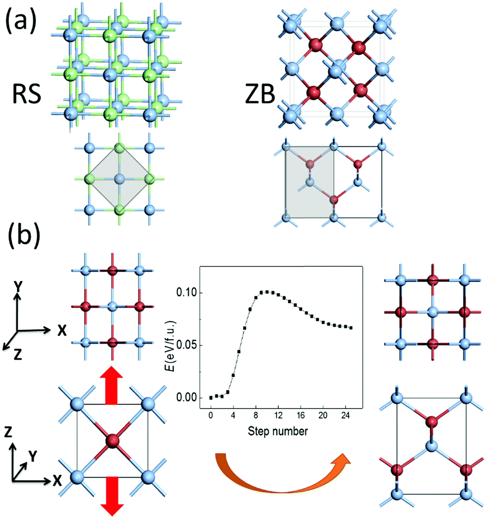 | ||
| Fig. 1 Geometric structures of (a) RS and ZB silver halide crystals, where smaller unit cells marked by the grey area are illustrated. (b) A possible pathway (middle panel) of the phase transition of AgBr from the RS (left panels) to ZB (right panels) structure, where the top view (upper panels) and side view (lower panels) are displayed. Blue, green, and brown spheres denote Ag, Cl, and Br/I atoms, and red thick arrows denote the strain directions. | ||
| AgCl | AgBr | AgI | CuCl | CuBr | NaCl | ZnS | ||
|---|---|---|---|---|---|---|---|---|
| ΔE (eV f.u.−1) | LDA | 0.09 | 0.07 | −0.07 | −0.31 | −0.30 | 0.27 | −0.54 |
| GGA | −0.05 | −0.08 | −0.19 | −0.35 | −0.36 | 0.14 | −0.63 | |
The ZB structure can be obtained by simultaneously displacing all halide anions in the RS structure to (¼, ¼, ¼), and the calculated pathway based on SSNEB (see Fig. S1, ESI†) shows a transition barrier of 0.17 eV f.u.−1 for AgBr. However, as we rotate the lattices of the RS and ZB structures by 45 degrees and adopt a smaller unit cell illustrated by the grey area in Fig. 1(a), the ZB structure can also be obtained by buckling the linear –M–X– chains in the RS structure. In view of the distinct lattice parameters and the small energy difference of the two phases, the phase transformation from RS to ZB can be induced by a tensile strain along the z axis by prolonging the lattice constant along −z with the vertical displacement of halide ions and buckling of –M–X– chains, as displayed in Fig. 1(b). For example, the calculated transition barrier is only 0.10 eV f.u.−1 for AgBr, where the ZB phase, only 0.07 eV f.u.−1 higher in energy, may become more stable upon application of a tensile strain. The ZB metastable phase might also be obtained via epitaxial growth on substrates with similar ZB structures and similar lattice constants, e.g., AgCl on Ge, or AgBr on InAs. However, compared with a tensile strain, which can be difficult to control uniformly, an external electric field may be a more feasible approach for inducing the phase transformation, noting that the ZB structure is polar (with alternating planes of cations and anions), while the RS structure is non-polar.
II. Ferroelasticity/multiferroicity
The ZB structure is non-centrosymmetric and thus a polarization might be spontaneously formed. The ZB structure of AgI can be viewed as bundles of AgI zigzag chains with their polarization along the z axis, as marked with red circles in Fig. 2(a), and the polarization may be switchable due to the relatively low switching barrier for those chains. We note that WZ ZnO also possesses a polar structure, but its polarization is not deemed as switchable due to its relatively high switching barrier of 0.25 eV f.u.−1.31 It only becomes ferroelectric in the form of ultra-thin multilayers as the associated barrier is lowered to 0.10 eV f.u.−1 due to the effect of the depolarization field.32 If this polarization can be reversed with the switching of AgI zigzag chains in a possible switching pathway from I to II (see Fig. 2(a)), the symmetrical RS phase can be the intermediate state (II) as the zigzag AgI chains become flat, with the halide anions moving along the z direction. The switching pathway is computed by using the SSNEB method as shown in Fig. 2(a), suggesting a low switching barrier of 0.14 eV f.u.−1 The latter is much lower than the switching barrier of PbTiO3 (∼0.20 eV f.u.−1). Meanwhile, a large polarization of 0.40 C m−2 is formed in ZB-AgI, based on our Berry-phase calculation, a value much greater than that in BaTiO3 (∼0.26 C m−2). The WZ phase of AgI (Fig. 2(b); 0.2 meV f.u.−1) is also polar with a polarization of 0.20 C m−2, while our SSNEB calculation of the pathway in Fig. 2(c) shows that the ferroelectric switching barrier can be as high as 0.27 eV f.u.−1, even higher than that for WZ ZnO (0.25 eV), making ferroelectric switching almost impossible under ambient conditions.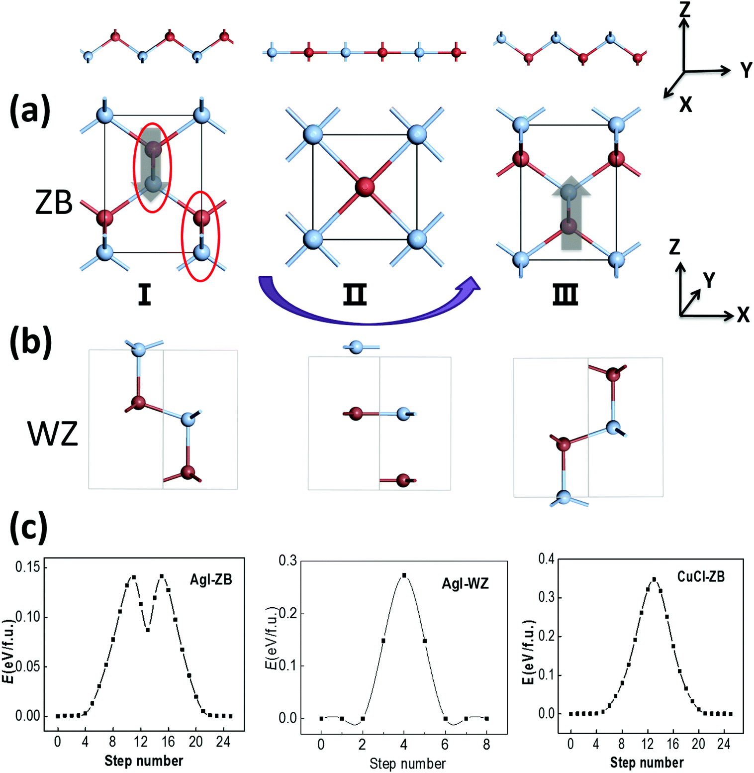 | ||
| Fig. 2 An illustration of the ferroelectric switching pathway of (a) ZB and (b) WZ AgI, where the top panels show that the zigzag chains in red circles (lower panels) in the initial state (I) become flat in the intermediate state (II), and are finally reversed in state III. Thick/grey arrows in (a) denote the directions of polarizations. (c) Calculated energy profiles of the switching pathways for ZB AgI, WZ AgI and ZB CuCl by using the SSNEB method. | ||
Similarly, for ZB CuCl, the computed switching pathway shows an even higher barrier of 0.35 eV f.u.−1, despite the calculated polarization is as high as 0.59 C m−2. However, this barrier is not necessarily the lowest one among all the possible switching pathways, which will be demonstrated later. Compared with AgI, the energy difference between the ZB and RS states of CuCl is much larger. The switching pathway of ZB AgI, with a local minimum and two transition states, indicates that the RS state is metastable, whereas for CuCl the RS state is the transition state.
Another possible switching pathway is also taken into consideration. As displayed in Fig. 3(a), the polar zigzag chains in the initial state (I) may also be switched from the −z to the −x or −y axis upon application of a horizontal electric-field, leading to a 90 degree polarization switching with a lattice rotation in the final state (III). Here, the zigzag chains are not flat like in Fig. 2(a), but can be switched by 90 degrees in the intermediate state (II). This transformation may also be obtained by a horizontal strain along the −x/−y direction with smaller lattice constants. Upon application of a strain or an electric field, the rotated and equivalent state III could be more favorable in energy. As a result, the transformation from I to III can be viewed as both ferroelastic switching and 90 degree ferroelectric switching, which may take place under ambient conditions if the switching barrier is within the desirable range (<0.15 eV). The symmetrical RS state could still be an intermediate state in a possible switching pathway, and the switching barrier could be moderate. According to our SSNEB calculation, a switching barrier of 0.13 eV f.u.−1 is obtained for the pathway of 90 degree switching for ZB AgI, which is slightly lower than the 180 degree switching barrier. The identified intermediate state, II, however, is a titled metastable structure that is 0.11 eV higher in energy than the ground state. As the polarization is switched to the −x/−y direction, the lattice constant in the −z direction is also swapped with the lattice constant in the −x/−y direction, so their ferroelectricity and ferroelasticity are coupled. The reversible strain, defined as (|c|/|a|−1) × 100%, will be as high as 41.6%.
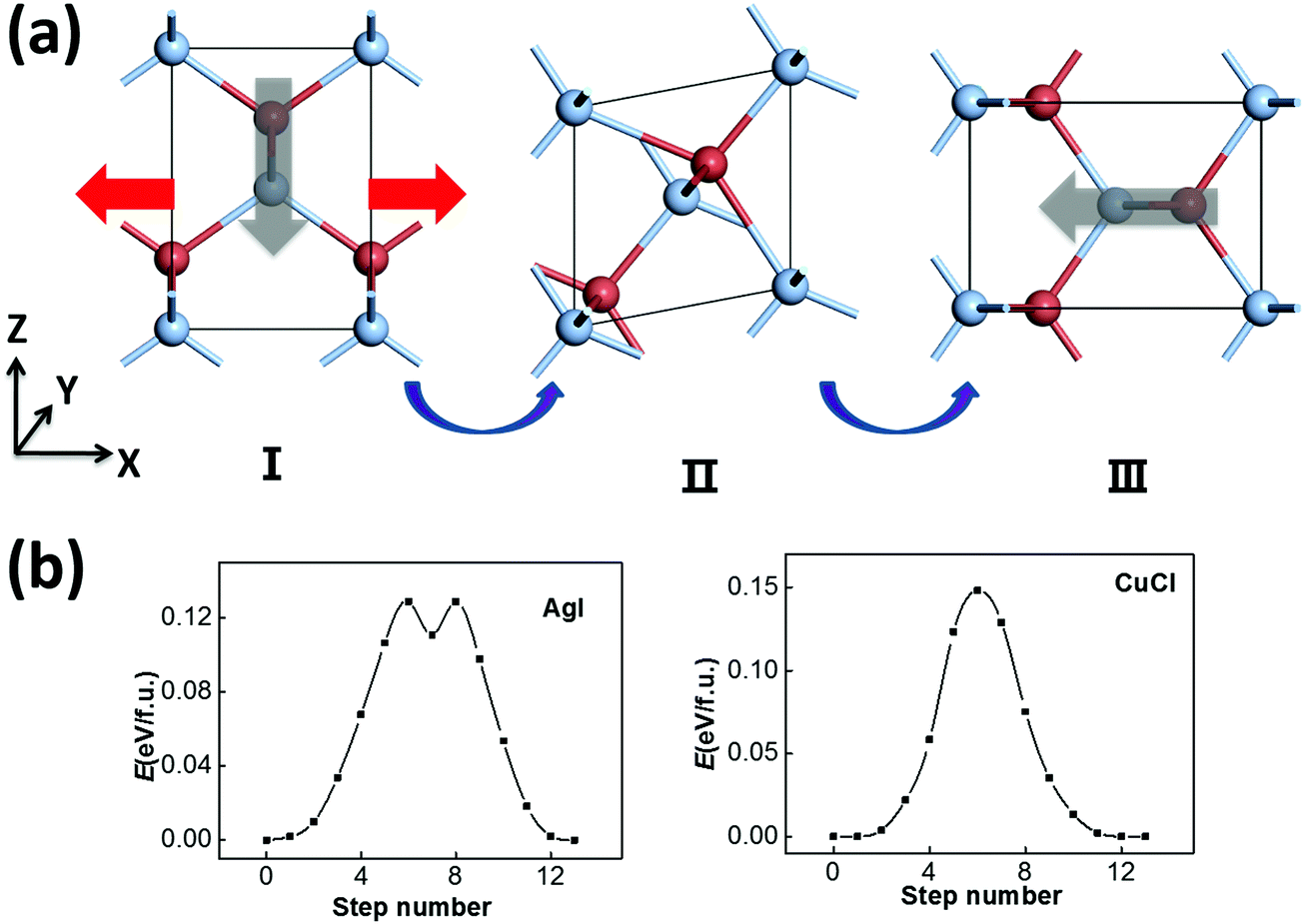 | ||
| Fig. 3 (a) The pathway of ferroelastic switching (90 degree ferroelectric switching) and (b) the calculated energy profiles based on the SSNEB method for AgI and CuCl. Here the zigzag chains in the initial state (I) are switched by 45 degrees in the intermediate state (II), and then by 90 degrees in state III. | ||
For the ferroelastic (90 degree ferroelectric) switching pathway of CuCl displayed in Fig. 3(b), the switching barrier of ∼0.15 eV f.u.−1 is much lowered compared with 180 degree ferroelectric switching. This is plausible as the intermediate state (II) maintains tetra-coordination for all atoms, which is energetically more favorable compared with the RS state for CuCl. Here, the 180 degree polarization switching can be achieved by repeating 90 degree switching twice, and this pathway is more favorable with a much lower barrier compared with the pathway in Fig. 2(c). As a result, CuCl can also be multiferroic under ambient conditions with coupled ferroelectricity and ferroelasticity.
The epitaxial growth of traditional ferroelectrics like perovskites on silicon is still challenging due to issues such as lattice mismatch, which hinders substitution of silicon-based RAMs with ferroelectric RAMs to be integrated with silicon wafers utilizing a mature silicon process. Having demonstrated a series of ZB multiferroic semiconductors in this study, we illustrate that CuCl and silicon have similar lattice constants (within 1% lattice mismatch) and structures to CuBr and germanium, as well as to ZB AgI and InSb. The lattice similarities have important implications for the epitaxial growth and combination with prevailing semiconductors like silicon, as shown in Fig. S2(a) (ESI†). According to previous experimental reports, both CuBr and AgI are wide-direct-gap semiconductors (band gaps in the range of 2.9–3.4 eV) with high mobility, while Ge and InSb are both narrow-gap semiconductors (0.2–0.7 eV).6,33 If the mixed alloy Cu1−xBr1−xGex or Ag1−xI1−xInxSbx can be achieved, in view of their similar lattice constants and structures, a chemical multi-junction model, as shown in Fig. S2(b) (ESI†), with a broad range of bandgaps might be built, which in principle can overpass the Shockley–Queisser detailed-balance limit of photovoltaic conversion efficiency for mono-bandgap semiconductors.34 The ferroelectric polarization may enhance the open-circuit voltage and the lifetime of excitons by hindering the recombination of electrons and holes.35,36
III. Two-dimensional monolayer polymorphs
We also explore the low-energy monolayer structures of silver/copper monohalides. After an extensive structure search based on the CALYPSO program, we obtained two stable structures, I and II, as displayed in Fig. 4(a) for each of CuCl, AgCl and AgBr. Structure I is composed of two buckled layers of honeycomb MX lattices, slightly lower in energy compared with structure II, which is composed of a buckled Cu/Ag monolayer covered with halides on the two surfaces. Similar but still different polymorph structures I and II for AgI/CuBr are also obtained, where structure I is composed of a buckled honeycomb Ag/Cu layer covered with I/Br atoms, with a slightly lower energy than the more symmetrical structure II (Fig. 4(b)), which is composed of a planar square Ag/Cu monolayer covered with I/Br atoms. As listed in Table 2, the energy differences between the bulk phase and the 2D polymorphs are around a tenth of eV f.u.−1, much smaller than that (0.43/0.26 eV f.u.−1 based on the LDA/GGA computation) of the highly ionic crystal of NaCl, or that (0.56/0.44 eV f.u.−1 based on the LDA/GGA computation) of the covalent crystal of ZnS. Fig. 4(c) displays a possible pathway of the phase transition from the bulk ZB phase to layered bulk polymorph (whose layer is the same as 2D polymorph II) phase, which can be viewed as the rotation of zigzag chains in the red circles. A barrier lower than 0.10 eV f.u.−1 for such a phase transition of CuCl is predicted based on the SSNEB calculations and LDA method. The negative values for CuCl and CuBr based on the GGA computation imply that some 2D polymorphs may be even more favorable in energy compared with the ZB phase of the bulk structure. Even based on LDA results, 2D polymorph II will become 0.016 eV f.u.−1 lower in energy compared with the ZB phase when half of the Cu atoms in CuCl are substituted with Ni atoms, as shown in Fig. 4(d).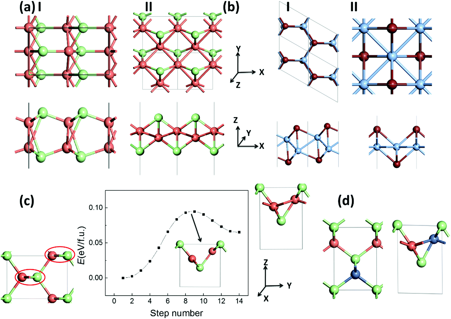 | ||
| Fig. 4 (a and b) Top views (upper panels) and side views (lower panels) of 2D polymorphs, I and II, for (a) CuCl/AgCl/AgBr and (b) AgI/CuBr. (c) Computed pathway (middle panel) of phase transition for CuCl from the bulk ZB (left panel) to a layered bulk polymorph (whose layer is the same as 2D polymorph II) (right panel) structure by using the LDA method. (d) A comparison of the bulk ZB (left panel) and layered bulk polymorph (right panel) structures of Cu0.5Ni0.5Cl. | ||
| AgCl | AgBr | AgI | CuCl | CuBr | ||
|---|---|---|---|---|---|---|
| ΔI (eV f.u.−1) | LDA | 0.17 | 0.12 | 0.05 | 0.11 | 0.04 |
| GGA | 0.07 | 0.05 | 0.035 | 0.02 | −0.01 | |
| ΔII (eV f.u.−1) | LDA | 0.24 | 0.15 | 0.08 | 0.13 | 0.07 |
| GGA | 0.13 | 0.08 | 0.05 | −0.01 | 0.00 | |
Synthesis of 2D monolayers is likely to be feasible, in view of the small energy difference shown in Table 2. As a comparison, the energy difference between bulk silicon and 2D silicene is notably much larger (0.76/0.65 eV f.u.−1 by LDA/GGA), and yet 2D silicene has been synthesized in the laboratory. Furthermore, the surfaces covered with halide anions also give rise to oxidation resistance and low cleavage energy of the layered structure: e.g., the cleavage energies from the layered bulk to monolayer structure for CuCl I and II are, respectively, 0.27 and 0.20 J m−2, even lower than that of graphite to graphene (0.3581 J m−2). We have further verified the dynamic stability of the 2D monolayers by computing their phonon dispersions, as shown in Fig. S3 (ESI†). All the vibration spectra are free of soft modes associated with structural instabilities.
As shown in Fig. 4(a), both 2D structures I and II for CuCl/AgCl/AgBr possess spontaneous in-plane polarization and strain, which may also be multiferroic if they are switchable. Similarly, their polar direction initially along the −x axis may be switched to the −y axis upon application of an electric-field, as displayed in Fig. 5(a and b), leading to a 90 degree polarization and lattice rotation. This transformation may also be obtained by an in-plane strain along the −y direction, so ferroelastic switching and 90 degree ferroelectric switching are equivalent. According to our SSNEB calculation, a switching barrier of 0.08 eV f.u.−1 is predicted for the pathway of ferroelastic switching for 2D CuCl polymorph I (Fig. 5(c)), about a half of the barrier height for bulk CuCl, as shown in Fig. 3(b). The 180 degree ferroelectric switching can be obtained by repeating 90 degree switching twice with the same switching barrier, and the switchable polarization of 2.8 × 10⁻¹⁰ C m−1 is even higher than those of 2D SnS and SnSe. As a result, 2D CuCl I can also be multiferroic under ambient conditions with coupled ferroelectricity and ferroelasticity. The switching barrier for polymorph II is even lower, as displayed in Fig. S4(a) (ESI†), and the switchable polarization is 1.5 × 10⁻¹⁰ C m−1. The band structures of both 2D polymorphs (Fig. 5(d and e)) are highly anisotropic, with distinct effective mass along Γ–X and Γ–Y, so their ferroelastic switching (90 degree ferroelectric switching) can be electrically detected. One may even obtain 2D triferroics37 by doping 3d magnetic elements. For example, polymorph II of CuCl becomes ferromagnetic when some of the Cu atoms are substituted with Ni atoms, as shown in Fig. S4(b) (ESI†). Each Ni atom possesses 1 μB magnetic moment, while the easy axis of magnetism and electrical polarization are both aligned in the same in-plane direction, which can also be switched by 90 degrees upon ferroelastic switching. As a result, their ferromagnetism, ferroelectricity and ferroelasticity are all coupled.
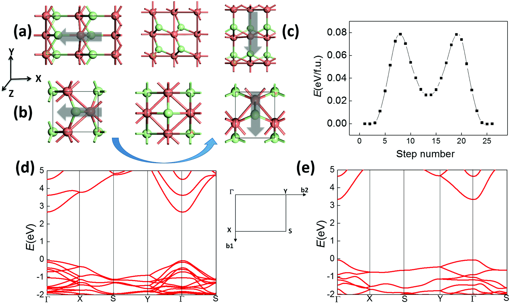 | ||
| Fig. 5 Ferroelastic switching (90 degree ferroelectric switching) of 2D polymorphs (a) I and (b) II of CuCl. (c) Calculated pathway of ferroelastic switching for polymorph I. Band structures of polymorphs (d) I and (e) II of CuCl are calculated based on the hybrid functional HSE06.38 | ||
In summary, through density-functional theory calculations we have demonstrated that the moderate barrier for the phase transition between bulk RS and ZB phases may give rise to ferroelectricity and ferroelasticity with relatively low switching barriers under ambient conditions. Some bulk halides even have similar lattice constants and structures to prevailing semiconductors like silicon, thereby making epitaxial growth a high possibility to potentially resolve a major issue of integrating traditional ferroelectrics into silicon-based circuits. Moreover, their stable 2D polymorphs are close or even lower in energy compared with their bulk phases, suggesting a high likelihood for successful synthesis of these 2D monolayers in the future. Some 2D monolayers are also predicted to be 2D multiferroics. As such, their coupled ferroelasticity and ferroelectricity together with anisotropic band structures are highly desired for efficient data reading and writing.
Conflicts of interest
The authors declare no competing financial interest.Acknowledgements
This work was supported by the National Natural Science Foundation of China (No. 21573084). XCZ was supported by the UNL Holland Computing Center.References
- J. F. Hamilton, Adv. Phys., 1988, 37, 359–441 CrossRef CAS.
- P. Wang, B. Huang, X. Qin, X. Zhang, Y. Dai, J. Wei and M.-H. Whangbo, Angew. Chem., 2008, 120, 8049–8051 CrossRef.
- Y. Bi and J. Ye, Chem. – Eur. J., 2010, 16, 10327–10331 CrossRef CAS PubMed.
- L. A. Palomino-Rojas, M. López-Fuentes, G. H. Cocoletzi, G. Murrieta, R. de Coss and N. Takeuchi, Solid State Sci., 2008, 10, 1228–1235 CrossRef CAS.
- S. Fujita, Organic Chemistry of Photography, Springer Berlin Heidelberg, Berlin, Heidelberg, 2004, pp. 59–74 Search PubMed.
- W. Gao, W. Xia, Y. Wu, W. Ren, X. Gao and P. Zhang, Phys. Rev. B, 2018, 98, 045108 CrossRef CAS.
- S. Hoshino, T. Sakuma and Y. Fujii, Solid State Commun., 1977, 22, 763–765 CrossRef CAS.
- R. C. Hanson, T. A. Fjeldly and H. D. Hochheimer, Phys. Status Solidi B, 1975, 70, 567–576 CrossRef CAS.
- Y. Li, L. J. Zhang, T. Cui, Y. W. Li, Y. Wang, Y. M. Ma and G. T. Zou, J. Phys.: Condens. Matter, 2008, 20, 195218 CrossRef.
- S. Hull and D. A. Keen, Phys. Rev. B: Condens. Matter Mater. Phys., 1999, 59, 750–761 CrossRef CAS.
- J. E. Maskasky, Phys. Rev. B: Condens. Matter Mater. Phys., 1991, 43, 5769–5772 CrossRef CAS.
- A. Zunger and M. L. Cohen, Phys. Rev. B: Condens. Matter Mater. Phys., 1979, 20, 1189–1193 CrossRef CAS.
- J. C. Phillips, Rev. Mod. Phys., 1970, 42, 317–356 CrossRef CAS.
- M. Wu and P. Jena, Wiley Interdiscip. Rev.: Comput. Mol. Sci., 2018, 8, e1365 Search PubMed.
- M. Wu, H. Fu, L. Zhou, K. Yao and X. C. Zeng, Nano Lett., 2015, 15, 3557–3562 CrossRef CAS PubMed.
- E. K. H. Salje, Annu. Rev. Mater. Res., 2012, 42, 265–283 CrossRef CAS.
- W. Li and J. Li, Nat. Commun., 2016, 7, 10843 CrossRef CAS PubMed.
- L. Kou, Y. Ma, C. Tang, Z. Sun, A. Du and C. Chen, Nano Lett., 2016, 16, 7910–7914 CrossRef CAS PubMed.
- C. Zhang, Y. Nie, S. Sanvito and A. Du, Nano Lett., 2019, 19, 1366–1370 CrossRef PubMed.
- S. Dong, J.-M. Liu, S.-W. Cheong and Z. Ren, Adv. Phys., 2015, 64, 519–626 CrossRef CAS.
- Q. Yang, W. Xiong, L. Zhu, G. Gao and M. Wu, J. Am. Chem. Soc., 2017, 139, 11506–11512 CrossRef CAS PubMed.
- M. Wu and X. C. Zeng, Nano Lett., 2016, 16, 3236–3241 CrossRef CAS PubMed.
- M. Wu and X. C. Zeng, Nano Lett., 2017, 17, 6309–6314 CrossRef CAS PubMed.
- G. Kresse and J. Furthmüller, Phys. Rev. B: Condens. Matter Mater. Phys., 1996, 54, 11169–11186 CrossRef CAS.
- P. E. Blöchl, Phys. Rev. B: Condens. Matter Mater. Phys., 1994, 50, 17953–17979 CrossRef.
- J. P. Perdew, K. Burke and M. Ernzerhof, Phys. Rev. Lett., 1996, 77, 3865–3868 CrossRef CAS PubMed.
- R. King-Smith and D. Vanderbilt, Phys. Rev. B: Condens. Matter Mater. Phys., 1993, 47, 1651 CrossRef CAS.
- D. Sheppard, P. Xiao, W. Chemelewski, D. D. Johnson and G. Henkelman, J. Chem. Phys., 2012, 136, 074103 CrossRef PubMed.
- Y. Wang, J. Lv, L. Zhu and Y. Ma, Comput. Phys. Commun., 2012, 183, 2063–2070 CrossRef CAS.
- Y. Wang, J. Lv, L. Zhu and Y. Ma, Phys. Rev. B: Condens. Matter Mater. Phys., 2010, 82, 094116 CrossRef.
- H. Moriwake, A. Konishi, T. Ogawa, K. Fujimura, C. A. J. Fisher, A. Kuwabara, T. Shimizu, S. Yasui and M. Itoh, Appl. Phys. Lett., 2014, 104, 242909 CrossRef.
- L. Li and M. Wu, ACS Nano, 2017, 11, 6382–6388 CrossRef CAS PubMed.
- F. Tran and P. Blaha, J. Phys. Chem. A, 2017, 121, 3318–3325 CrossRef CAS PubMed.
- M. Wu, X. Qian and J. Li, Nano Lett., 2014, 14, 5350–5357 CrossRef CAS PubMed.
- S. Y. Yang, J. Seidel, S. J. Byrnes, P. Shafer, C. H. Yang, M. D. Rossell, P. Yu, Y. H. Chu, J. F. Scott, J. W. Ager Iii, L. W. Martin and R. Ramesh, Nat. Nanotechnol., 2010, 5, 143 CrossRef CAS PubMed.
- F. Wang, I. Grinberg, L. Jiang, S. M. Young, P. K. Davies and A. M. Rappe, Ferroelectrics, 2015, 483, 1–12 CrossRef CAS.
- L. Yang, M. Wu and K. Yao, Nanotechnology, 2018, 29, 215703 CrossRef PubMed.
- J. Heyd, G. E. Scuseria and M. Ernzerhof, J. Chem. Phys., 2003, 118, 8207–8215 CrossRef CAS.
Footnote |
| † Electronic supplementary information (ESI) available. See DOI: 10.1039/c9nh00172g |
| This journal is © The Royal Society of Chemistry 2019 |