
Ultrafast free carrier dynamics in black phosphorus–molybdenum disulfide (BP/MoS2) heterostructures†
Zhonghui
Nie
ab,
Yuhan
Wang
ab,
Ziling
Li
c,
Yue
Sun
a,
Shuchao
Qin
a,
Xiaoping
Liu
d,
I. C. E.
Turcu
a,
Yi
Shi
a,
Rong
Zhang
a,
Yu
Ye
 c,
Yongbing
Xu
*a,
Giulio
Cerullo
*ef and
Fengqiu
Wang
*ab
c,
Yongbing
Xu
*a,
Giulio
Cerullo
*ef and
Fengqiu
Wang
*ab
aSchool of Electronic Science and Engineering, Nanjing University, Nanjing 210023, China. E-mail: fwang@nju.edu.cn; ybxu@nju.edu.cn
bKey Laboratory of Intelligent Optical Sensing and Manipulation, Ministry of Education, Nanjing University, Nanjing 210093, China
cDepartment of Physics, Peking University, Beijing 100871, China
dCollege of Engineering and Applied Sciences, Nanjing University, Nanjing 210093, China
eDipartimento di Fisica, Politecnico di Milano, Piazza Leonardo da Vinci 32, I-20133 Milano, Italy. E-mail: giulio.cerullo@fisi.polimi.it
fIstituto di Fotonica e Nanotecnologie (IFN), CNR, Piazza Leonardo da Vinci 32, I-20133 Milano, Italy
First published on 8th April 2019
Abstract
Investigation and manipulation of photocarrier dynamics in van der Waals (vdW) heterostructures with type-II band alignment have gained much interest because of their fundamental and technological significance. Despite remarkable progresses on the ultrafast dynamics of interlayer excitons in transition metal dichalcogenide (TMD) heterostructures, transient behaviors of free photocarriers in vdW heterostructures, which is a critical process governing the performance of optoelectronic devices, remain poorly understood, restricting their effective manipulation. In this study, ultrafast dynamics of photo-generated free carriers in a type-II black phosphorus–molybdenum disulfide (BP/MoS2) heterostructure was investigated. A remarkably reduced lifetime (∼5 ps) of interlayer electron–hole (e–h) recombination was found, compared with those of BP film (∼130 ps) and other exciton-rich TMD heterostructures. More interestingly, this ultrafast interlayer recombination process can well be described by the Langevin model, and this high recombination rate is fundamentally linked to the high carrier mobility in BP. In addition, broadband measurements reveal that the interlayer recombination rate is independent of the broad energy distribution of photocarriers. Our findings provide new important and complementary insights into the fundamental photo-physics of vdW heterostructures, and represent a novel proposal for designing broadband high-speed optoelectronic devices.
New conceptsvan der Waals (vdW) heterostructures with type-II band alignment hold great promise for applications in the fields of optoelectronics, photonics and spin-valleytronics. Photocarrier dynamics in such systems has been actively studied for guidance on improving the device performance. However, current research efforts mostly focus on (interlayer) excitons, while it is the free carriers that ultimately determine the photocurrent and critically affect the performance of photo-sensitive devices. In addition, the rarely studied free carrier dynamics may offer complementary insights that may help elucidate the rather complicated exciton dynamics. Herein, we investigated the ultrafast dynamics of photo-generated free carriers in a type-II vdW heterostructure, constructed by black phosphorus (BP) and molybdenum disulfide (MoS2). An unusually fast interlayer recombination (∼5 ps) of unbound photocarriers has been identified, which can be well described by a simple Langevin model. The large recombination rate was found to be fundamentally linked to the high carrier mobility in BP, suggesting effective pathways for carrier lifetime tuning. The present study not only reveals generic free carrier dynamics in 2D semiconductor heterostructures, but also provides new perspectives for interpreting the exciton dynamics in vdW heterostructures, both of which are crucial for designing high-speed novel devices based on 2D materials. |
Introduction
van der Waals (vdW) heterostructures with a type-II band alignment,1,2 formed by stacks of two-dimensional (2D) materials, have attracted considerable attention in recent years as excellent platforms to explore exotic physics3–9 and novel atomically thin devices.10–14 A comprehensive understanding of the dynamic evolution of photocarriers in vdW heterostructures is a prerequisite to control and optimize the performance of similar types of optoelectronic devices, on which rapid advancements have been achieved.15–23 On short timescales (<1 ps), the photo-generated charge carriers travel across the interface due to the built-in field within several tens of femtoseconds regardless of the relative crystallographic alignment;16,20–23 on longer timescales (>1 ps), the separated photocarriers recombine on a timescale varying from picoseconds to nanoseconds.18,19,22 However, so far most experimental investigations focus on the charge transfer and recombination dynamics of interlayer excitons in transition metal dichalcogenide (TMD) heterostructures,16,18–23 while, in fact, the photocurrent in most optoelectronic devices arises from free carriers, and the interlayer exciton cannot generate photocurrent unless it dissociates into free carriers.10–14,24,25 In addition, most existing theoretical models10,23 on the recombination dynamics do not fully account for the excitonic effect in low-dimensional materials4,9,26–28 and a number of experimental observations in the exciton-rich heterostructures remain to be elucidated.20,22,29 Moreover, a heterostructure supporting free carriers may be more precisely depicted by present theoretical mechanisms and the obtained complementary insights could be useful for explaining the relatively complicated dynamics of exciton-dominated systems. To the best of our knowledge, so far, there have been few investigations on the dynamic behaviours of free carriers in 2D semiconductor heterostructures.Herein, we chose to experimentally investigate the photocarrier dynamics of a vdW heterostructure supporting free carriers, i.e., a black phosphorus–molybdenum disulfide (BP/MoS2) heterostructure with a type-II band alignment, as shown in the top panel of Fig. 1(a).30,31 Compared with TMDs, the binding energy between charge carriers in BP films is much weaker (<40 meV) and unbound (quasi-)free carriers can be directly injected by optical excitation,32,33 as shown in Fig. 1(a). In addition, BP-based vdW heterostructures are capable of extending the spectral range of 2D optoelectronic devices into the infrared (IR) range.32,34–38 The direct and tunable bandgap spanning from visible to mid-IR, together with its much higher carrier mobility compared with TMDs and the anisotropy of physical properties, makes BP a promising candidate for 2D optoelectronic and photonic devices especially for the IR range.34–40
 | ||
| Fig. 1 (a) Illustration of the band alignment of the BP/MoS2 heterostructure, which belongs to the type-II heterostructure. Such a band structure can easily separate electrons and holes into different layers. (b) Optical microscope image of the BP/MoS2 heterostructure, where the blue and yellow lines outline the BP film and the bilayer MoS2 respectively. The scale bar is 20 μm. It should be noted that a thin hBN film (not marked) was used to protect the BP film from degradation. (c) Photoluminescence spectra of MoS2 and the heterostructure under 514 nm laser excitation. PL quenching has been observed, which is attributed to interlayer charge transfer in the heterostructure. | ||
In this study, femtosecond transient absorption spectroscopy was employed to investigate the dynamics of photo-generated free carriers in the BP/MoS2 heterostructure. In addition to ultrafast electron transfer to MoS2 upon photoexciting the BP film, an unusually short lifetime of ∼5 ps of the transferred electrons was identified, which was much shorter than those of the constituent materials and the exciton-dominated heterostructures. Combining with the probing of the lifetime of holes remaining in the BP film, we found that this fast decay of interlayer free carriers can be well described by the Langevin model. The significant reduction in lifetime (from hundreds of picoseconds to several picoseconds) can be understood by considering a dramatically enhanced Langevin constant, caused by the high hole mobility of BP. Furthermore, broadband pump–probe spectroscopy demonstrates that the interlayer recombination rate of the free photocarriers is independent of their energy distribution. Our results suggest that in contrast to that of the exciton-dominated systems, the free carrier dynamics in 2D semiconductor heterostructures can be reasonably well depicted by a simple Langevin model. A new strategy is found to drastically reduce the photocarrier lifetime through engineering the Langevin constant at the heterointerface, which may have practical implications for designing broadband high-speed optoelectronic and photovoltaic devices based on 2D heterostructures.
Experimental
The BP and the MoS2 films were mechanically exfoliated and stacked onto a silicon substrate with a 280 nm oxide layer to form a heterostructure, as shown in Fig. 1(b). To avoid the degradation of the BP film, a thin boron nitride (BN) film was used to cover the whole heterostructure. The thicknesses of the BP and MoS2 films are ∼8 and 1.1 nm, respectively, as measured by atomic force microscopy (AFM), as shown in Fig. S1 (ESI†). The number of layers of the BP film is estimated to be ∼15, corresponding to a bandgap of 0.3 eV and a binding energy below 40 meV.33,35,41 The layer thickness measured for the MoS2 film is close to that of the bilayer sample (1.3 nm) and the difference between E12g and A1g Raman modes (shown in Fig. S2, ESI†) is about 23 cm−1, indicating that the sample is bilayer MoS2.4,42 The Raman spectra of the BP film, bilayer MoS2 and the heterostructure are presented in Fig. S3 (ESI†). These Raman modes associated with the individual materials have also been observed in the region of the heterostructure, which is consistent with previous reports31,36 and suggests a good sample quality. In addition, as the A2g mode of the BP film originates from the in-plane atomic motion, its Raman intensity exhibits polarization dependence.43 The crystal orientation of the BP film can be easily identified through polarization-dependent Raman spectroscopy, as reported in Fig. S4 (ESI†). The photoluminescence (PL) spectra of the bilayer MoS2 and the heterostructure are presented in Fig. 1(c). The peaks at 680 nm and 620 nm of the MoS2 (red line) arise from the A and B excitons.4,42 Noticeable reduction (∼30%) in the PL intensity has been observed in the heterostructure region, which is a typical signature for charge transfer in type-II heterostructures.30,31 The ∼30% decrease is not significant compared with that of other TMD-based heterostructures, and the main reasons could be the low PL efficiency of the bilayer MoS2 and the blocking of photo-excited hole transfer from MoS2 to the BP film by the majority carriers in the BP film (holes) with high density.36,39The ultrafast photocarrier response of the BP/MoS2 heterostructure was directly monitored by transient differential reflection spectroscopy (details in Fig. S5 and supplementary note 1, ESI†). An 800 nm (1.55 eV) linearly polarized laser, with 100 fs pulse duration, worked as the pump beam to excite photocarriers in the heterostructure. Due to the energy band alignment as well as the layer thickness, pump pulses should primarily be absorbed by the BP film, as confirmed by our experiments on the MoS2 bilayer.4,42,44 Using a 0.4%/nm absorption rate at 800 nm for BP films41 and assuming that each absorbed photon excites one e–h pair, the peak density of photocarriers excited in the BP film can reach a value of ∼1012 cm−2, and these photocarriers should be free carriers rather than excitons considering the low binding energy inside the BP film. To observe the electron transfer from the conduction band (CB) of the BP film to the CB of MoS2, we adopted a 620 nm laser to probe the dynamic behaviours of electrons in MoS2, as illustrated in Fig. 2(a). As the photon energy of the pump pulse (1.55 eV) is smaller than that of the probe pulse (2 eV) and the absorption gap of MoS2 (1.88 eV), individual BP and MoS2 films yielded no detectable signals, as shown in Fig. 2(b). However, an ultrafast and intense photo-bleaching (PB) signal can be observed in the heterostructure region, depicted by the black dots in Fig. 2(b). While the ultrafast interlayer electron transfer is not directly resolvable due to the limited instrumental response (∼300–400 fs),16,20,22,45 a remarkable observation is the extremely short carrier relaxation time of ∼5 ± 0.2 ps. (Single-exponential fitting is shown by the red line in Fig. 2(b).) Such a short lifetime is not only at least one order of magnitude faster than the intrinsic lifetimes of photocarriers in individual MoS2 and BP film (as shown in Fig. S6, ESI†),18,22,41,46–48 but also strikingly distinct from those of the long-lived interlayer excitons in the TMD heterostructures.18,22 To explore the origin of such a fast relaxation process, power-dependent measurements were performed. We extracted the peak values of the ΔR/R signal from the dynamic curves and summarized them as a function of pump fluence, as illustrated in the top panel of Fig. 2(c). Clearly, below the pump fluence of ∼80 μJ cm−2 (photocarrier density of ∼1013 cm−2), the transient signal increases linearly with the incident power density, while for higher fluences, it displays a saturation behavior.38,43,44 Interestingly, the lifetime of the transferred electrons in MoS2 stays almost constant (∼5 ps) (shown in the bottom panel of Fig. 2(c)), and exhibits negligible dependence on injected photocarrier density even beyond the linear region, indicating that such a short electron lifetime should not arise from trapping by interfacial defects.49
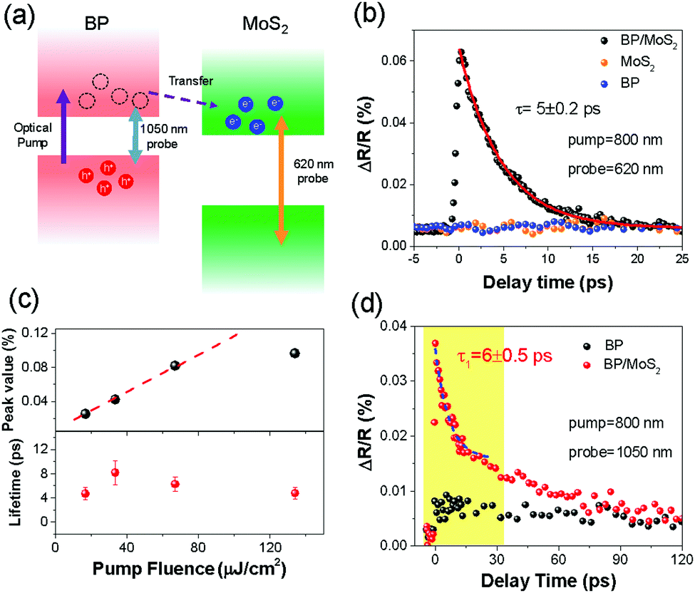 | ||
| Fig. 2 (a) Schematic illustrating the transient processes occurring in a BP/MoS2 heterostructure when the probe wavelengths are 620 nm and 1050 nm, respectively. (b) Transient reflectivity signals of the BP/MoS2 heterostructure and its constituent layers when pumped at 800 nm and probed at 620 nm. The ultrafast signal build-up of the heterostructure proves the existence of electron transfer, and the ∼5 ps relaxation time is much shorter than those of photocarriers in individual MoS2 and BP. (c) Pump-fluence dependence of the maximum ΔR/R signal (top) and lifetime (bottom) when the pump and probe wavelengths are 800 nm and 620 nm, respectively. (d) Time-resolved differential reflection measured for the BP film and BP/MoS2 heterostructure with an 800 nm pump and a 1050 nm probe. | ||
To reveal more details of the relaxation mechanisms, we changed the probe wavelength to 1050 nm (∼1.2 eV) while fixing the pump wavelength at 800 nm. As its photon energy is far below the bandgap of MoS2, the probe pulse then primarily detected transient signals from holes in the BP film, as is illustrated by Fig. 2(a). The measured transient signals of the BP film and the heterostructure are presented in Fig. 2(d). The transient signal of the BP film can be well fitted by a time constant of 130 ps (see Fig. S6, ESI†), which is in agreement with the previously reported lifetime of free carriers in BP.41,47,48 Moreover, a much stronger PB signal has been observed for the heterostructure, as shown in Fig. 2(d), whose magnitude is comparable to the signal induced by transferred electrons in MoS2 (Fig. 2(b)), and three to four times larger than that of the individual BP film. Such large enhancement in the signal is tentatively ascribed to the increase in the screening effect and a similar phenomenon has also been found in a graphene/WS2 heterostructure.17 Noticeably, a fast relaxation component (yellow-shaded area) clearly emerges in the dynamic curve of the heterostructure with a time constant of ∼6 ± 0.5 ps, well corresponding to the lifetime of hole population in the BP film. It should be noted that the observed ultrashort lifetime of holes in BP films coincides with that of the transferred electrons in MoS2, which strongly suggests that there exists an efficient bimolecular recombination process between photocarriers across the interface.
In the vdW heterostructures, there are two mechanisms potentially contributing to this unusual interlayer e–h recombination: the Shockley–Read–Hall (SRH) recombination (assisted by traps or defect states) and Langevin recombination (mediated by interlayer Coulomb interaction), as illustrated in Fig. 3(a).10,50,51 The coexistence of these two mechanisms has previously been reported in the TMD heterostructure devices, and both of them made significant contributions to the interlayer recombination, significantly affecting the generation of photocurrent and the efficiency of photon–electron conversion.10–14 In our case, the trap-assisted SRH recombination can be ruled out as the dominant process by the observed pump fluence-independence of photocarrier lifetimes. In contrast, the Langevin model describing the simultaneous recombination between electrons and holes is more consistent with our observations in Fig. 2. The Langevin model could be applicable here with another important reason being the enhanced Coulomb interaction between photocarriers confined in low-dimensional systems.
 | ||
| Fig. 3 (a) Two potential interlayer recombination mechanisms. In the top panel, the blue and purple arrows indicate the SRH and Langevin recombination processes, respectively. The circle in the bottom panel conceptually marks the Coulomb radius, according to the Langevin model, of an electron at the heterointerface. The dashed arrows point to an interfacial defect, which may act as a SRH recombination centre for charge carriers. (b) Transient signals when pump = 800 nm and probe = 620 nm measured at different pump fluences. The dashed blue lines are the fitting results using the rate equation based on the Langevin model (eqn S(1), ESI†). | ||
The rate equation based on the Langevin recombination can be expressed as:10,50

Therefore, we attributed the observed ultrashort lifetime of photocarriers at the BP/MoS2 interface to an efficient Langevin recombination process, with contributions from high (intrinsic) carrier densities in the two constituent materials and a large recombination constant B. Our findings indicate that the carrier density and mobility as well as the binding degree of photocarriers together determine the photocarrier dynamics in the BP/MoS2 heterostructure, which could provide effective approaches for tailoring the photocarrier lifetime in a type-II 2D heterostructure and the photo-response of related optoelectronic devices, e.g., gate-control,53 chemical doping54 or substrate-induced screening.53 Further experimental and theoretical studies may be useful to clarify the effects from other potential contributing mechanisms, such as interlayer coupling or electronic-state hybridization.55
To further investigate the energy distribution of transferred electrons and its influence on the Langevin recombination dynamics, broadband ultrafast spectroscopy was performed. The probe wavelength was tuned from 550 nm (2.25 eV) to 675 nm (1.84 eV), covering the A and B excitonic peaks of MoS2, while the pump wavelength was fixed at 800 nm. The measured differential reflectivity dynamics of the BP/MoS2 heterostructure are shown in Fig. 4(a), with the red lines indicating the single-exponential fittings. First, the observation of transient signals for all probe wavelengths suggests that the transferred electrons occupy a broad spread of energy states in the CB of MoS2. This phenomenon agrees with some recent theoretical and experimental results, where hot electrons are able to travel from the conduction band minimum (CBM) of one layer to energy levels above the CBM of the other layers.29,56 Interestingly, for the first time, broadband PB signals are observed, in contrast to the alternation between photo-absorption (PA) and PB as a result of the broadening and redshifting of the exciton absorption in TMD heterostructures. Second, the excess energy available to the transferred electrons could induce a thermalization process. The peak values of the transient signals in Fig. 4(a) are extracted and plotted as a function of the probe wavelengths in Fig. 4(b). The trend in the peak values roughly follows that of the PL spectrum of MoS2 (the black solid line), confirming that the thermal distribution of electrons is established on an ultrafast timescale.56,57 These observations mean that the ultrashort rising time (300–400 fs) in Fig. 4(a) covers both the electron transfer and thermalization processes. Then, we examined the relationship between the electron lifetime and the probe wavelength, as shown in Fig. 4(c). Interestingly, the lifetime varying between 5 ps and 8 ps shows no obvious dependence on the probe wavelength, which suggests that the rate of the interlayer Langevin recombination is not sensitive to the kinetic energy of electrons. Besides the energy distribution, we also investigated the polarization dependence of the transferred electrons and found that the anisotropy of photocarriers in the heterostructure has been partially weakened, compared with that of an individual BP film (supplementary note 3, ESI†).
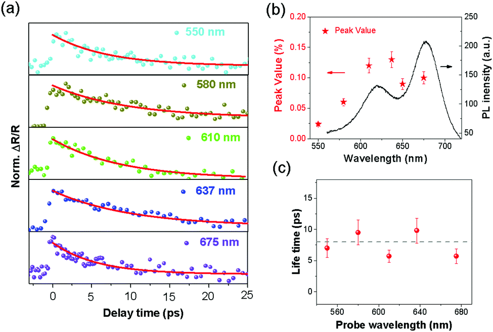 | ||
| Fig. 4 Broadband ultrafast nonlinear optical properties of BP/MoS2 heterostructure. (a) The ultrafast pump–probe measurements with a probe wavelength varying from 550 nm to 675 nm, covering the A and B exciton peaks, when the pump wavelength is fixed at 800 nm. Coloured dots are experimental data and red solid lines correspond to single-exponential fitting results. (b) Peak values of ΔR/R signal in the heterostructure under different probe wavelengths (red stars, left axis), extracted from (a). For comparison, the PL spectrum (black line, right axis) of the bilayer MoS2 is also drawn, suggesting that exciton states in MoS2 may affect the distribution of the transferred electrons. (c) The lifetime extracted from signals in (a) by single-exponential fitting as a function of probe wavelength. The lifetime of the heterostructure remains insensitive to the change of probe wavelength. | ||
Combining all our measurements, the transient photocarrier process in the BP/MoS2 heterostructure can be characterized by three major steps: the generation of hot e–h pairs in BP through optical excitation; ultrafast interlayer charge separation (electrons travel to the MoS2 layers, while holes are left behind in the BP layers) and thermalization (redistribution among the CB of MoS2) within few hundreds of femtoseconds, and finally the Langevin recombination between the separated electrons and holes in different layers on a timescale of ∼5 ps. The response time of the BP-based photodetectors is generally limited by the intrinsic lifetime of photocarriers (up to hundreds of picoseconds) and such a significant reduction in the photocarrier lifetime in the BP/MoS2 heterostructure, close to that of graphene,58 makes it possible to construct BP-based heterostructures to realize novel IR photo-sensitive devices with high speed.
Conclusions
In conclusion, we have investigated the ultrafast dynamics of photoexcited free carriers in a BP/MoS2 heterostructure by two-color ultrafast pump–probe optical spectroscopy. In addition to observing ultrafast charge transfer, we found an unusually short lifetime of ∼5 ps of the interlayer photocarriers, significantly shorter than those of pure BP film and TMD heterostructures. Supported by experimental and theoretical analysis, we attributed the observed ultrafast relaxation of interlayer free carriers to the Langevin recombination with a significantly enhanced Langevin constant B, due to the much higher hole mobility in BP. Moreover, broadband measurements revealed a relatively broad energy distribution of the transferred electrons in MoS2. The broadband PB signals with similar lifetimes demonstrated the energy-independent recombination processes of interlayer free carries. Our findings provide new insights into the fundamental photo-physics in vdW heterostructures and point out a new route to dramatically shorten photocarrier lifetimes at the 2D heterointerface, promoting the development of ultrafast optoelectronic devices in the IR range.Authors’ contributions
F. W., G. C. and Y. X. conceived the project and provided the experimental analysis. Z. N. and Y. W. performed the ultrafast measurements and basic characterizations of the samples; Z. L. and Y. Y. prepared the samples; Y. S., S. Q., X. L., E. T., Y. S. and R. Z. provided help and useful advice during ultrafast measurements. The manuscript was written through contributions of all authors. All authors have given approval to the final version of the manuscript.Conflicts of interest
There are no conflicts to declare.Acknowledgements
This work was supported by The State Key Project of Research and Development of China (2017YFA0206304); National Basic Research Program of China (2014CB921101, 2011CB301900); National Natural Science Foundation of China (61775093, 61427812); National Young 1000 Talent Plan; A ‘Jiangsu Shuangchuang Team’ Program; Natural Science Foundation of Jiangsu Province (BK20170012). And G. C. also acknowledged support by the European Union's Horizon 2020 Research and Innovation Program under grant agreement no. 785219 (GrapheneCore2).References
- A. K. Geim and I. V. Grigorieva, Nature, 2013, 499, 419–425 Search PubMed.
- K. S. Novoselov, A. Mishchenko, A. Carvalho and A. H. Castro Neto, Science, 2016, 353, aac9439 CrossRef CAS PubMed.
- L. Britnell, R. M. Ribeiro, A. Eckmann, R. Jalil, B. D. Belle, A. Mishchenko, Y. J. Kim, R. V. Gorbachev, T. Georgiou, S. V. Morozov, A. N. Grigorenko, A. K. Geim, C. Casiraghi, A. H. Castro Neto and K. S. Novoselov, Science, 2013, 340, 1311–1314 Search PubMed.
- K. F. Mak, C. Lee, J. Hone, J. Shan and T. F. Heinz, Phys. Rev. Lett., 2010, 105, 136805 CrossRef PubMed.
- C. R. Dean, L. Wang, P. Maher, C. Forsythe, F. Ghahari, Y. Gao, J. Katoch, M. Ishigami, P. Moon, M. Koshino, T. Taniguchi, K. Watanabe, K. L. Shepard, J. Hone and P. Kim, Nature, 2013, 497, 598–602 CrossRef CAS PubMed.
- E. Wang, X. Lu, S. Ding, W. Yao, M. Yan, G. Wan, K. Deng, S. Wang, G. Chen, L. Ma, J. Jung, A. V. Fedorov, Y. Zhang, G. Zhang and S. Zhou, Nat. Phys., 2016, 12, 1111–1115 Search PubMed.
- C. Jin, J. Kim, J. Suh, Z. Shi, B. Chen, X. Fan, M. Kam, K. Watanabe, T. Taniguchi, S. Tongay, A. Zettl, J. Wu and F. Wang, Nat. Phys., 2016, 13, 127–131 Search PubMed.
- J. Zhang, J. Wang, P. Chen, Y. Sun, S. Wu, Z. Jia, X. Lu, H. Yu, W. Chen, J. Zhu, G. Xie, R. Yang, D. Shi, X. Xu, J. Xiang, K. Liu and G. Zhang, Adv. Mater., 2016, 28, 1950–1956 CrossRef CAS PubMed.
- A. Raja, A. Chaves, J. Yu, G. Arefe, H. M. Hill, A. F. Rigosi, T. C. Berkelbach, P. Nagler, C. Schuller, T. Korn, C. Nuckolls, J. Hone, L. E. Brus, T. F. Heinz, D. R. Reichman and A. Chernikov, Nat. Commun., 2017, 8, 15251 Search PubMed.
- C. H. Lee, G. H. Lee, A. M. van der Zande, W. Chen, Y. Li, M. Han, X. Cui, G. Arefe, C. Nuckolls, T. F. Heinz, J. Guo, J. Hone and P. Kim, Nat. Nanotechnol., 2014, 9, 676–681 CrossRef CAS PubMed.
- F. Barati, M. Grossnickle, S. Su, R. K. Lake, V. Aji and N. M. Gabor, Nat. Nanotechnol., 2017, 12, 1134–1139 CrossRef CAS PubMed.
- M. M. Furchi, A. Pospischil, F. Libisch, J. Burgdorfer and T. Mueller, Nano Lett., 2014, 14, 4785–4791 Search PubMed.
- M. Long, E. Liu, P. Wang, A. Gao, H. Xia, W. Luo, B. Wang, J. Zeng, Y. Fu and K. Xu, Nano Lett., 2016, 16, 2254–2259 CrossRef CAS PubMed.
- H. Xue, Y. Wang, Y. Dai, W. Kim, H. Jussila, M. Qi, J. Susoma, Z. Ren, Q. Dai, J. Zhao, K. Halonen, H. Lipsanen, X. Wang, X. Gan and Z. Sun, Adv. Funct. Mater., 2018, 28, 1804388 CrossRef.
- C. Jin, E. Y. Ma, O. Karni, E. C. Regan, F. Wang and T. F. Heinz, Nat. Nanotechnol., 2018, 13, 994–1003 CrossRef CAS PubMed.
- X. Hong, J. Kim, S. F. Shi, Y. Zhang, C. Jin, Y. Sun, S. Tongay, J. Wu, Y. Zhang and F. Wang, Nat. Nanotechnol., 2014, 9, 682–686 Search PubMed.
- J. He, N. Kumar, M. Z. Bellus, H. Y. Chiu, D. He, Y. Wang and H. Zhao, Nat. Commun., 2014, 5, 5622 CrossRef CAS PubMed.
- P. Rivera, J. R. Schaibley, A. M. Jones, J. S. Ross, S. Wu, G. Aivazian, P. Klement, K. Seyler, G. Clark, N. J. Ghimire, J. Yan, D. G. Mandrus, W. Yao and X. Xu, Nat. Commun., 2015, 6, 6242 CrossRef CAS PubMed.
- F. Ceballos, M. Z. Bellus, H. Y. Chiu and H. Zhao, ACS Nano, 2014, 8, 12717–12724 Search PubMed.
- Z. Ji, H. Hong, J. Zhang, Q. Zhang, W. Huang, T. Cao, R. Qiao, C. Liu, J. Liang, C. Jin, L. Jiao, K. Shi, S. Meng and K. Liu, ACS Nano, 2017, 11, 12020–12026 CrossRef CAS PubMed.
- F. Ceballos, M. G. Ju, S. D. Lane, X. C. Zeng and H. Zhao, Nano Lett., 2017, 17, 1623–1628 Search PubMed.
- H. Zhu, J. Wang, Z. Gong, Y. D. Kim, J. Hone and X. Y. Zhu, Nano Lett., 2017, 17, 3591–3598 CrossRef CAS PubMed.
- Q. Zheng, W. A. Saidi, Y. Xie, Z. Lan, O. V. Prezhdo, H. Petek and J. Zhao, Nano Lett., 2017, 17, 6435–6442 CrossRef CAS PubMed.
- G. Lee, S. J. Pearton, F. Ren and J. Kim, ACS Appl. Mater. Interfaces, 2018, 10, 10347–10352 Search PubMed.
- T. Hong, B. Chamlagain, T. Wang, H. J. Chuang, Z. Zhou and Y. Q. Xu, Nanoscale, 2015, 7, 18537–18541 RSC.
- P. Kambhampati, Acc. Chem. Res., 2011, 44, 1–13 CrossRef CAS PubMed.
- P. Kambhampati, J. Phys. Chem. C, 2011, 115, 22089–22109 CrossRef CAS.
- P. Kambhampati, J. Phys. Chem. Lett., 2012, 3, 1182–1190 CrossRef CAS.
- X. Zhu, N. R. Monahan, Z. Gong, H. Zhu, K. W. Williams and C. A. Nelson, J. Am. Chem. Soc., 2015, 137, 8313–8320 CrossRef CAS PubMed.
- Y. Deng, Z. Luo, N. J. Conrad, H. Liu, Y. Gong, S. Najmaei, P. M. Ajayan, J. Lou, X. Xu and P. D. Ye, ACS Nano, 2014, 8, 8292–8299 CrossRef CAS PubMed.
- J. Yuan, S. Najmaei, Z. Zhang, J. Zhang, S. Lei, P. M. Ajayan, B. I. Yakobson and J. Lou, ACS Nano, 2015, 9, 555–563 Search PubMed.
- L. Li, J. Kim, C. Jin, G. J. Ye, D. Y. Qiu, F. H. da Jornada, Z. Shi, L. Chen, Z. Zhang, F. Yang, K. Watanabe, T. Taniguchi, W. Ren, S. G. Louie, X. H. Chen, Y. Zhang and F. Wang, Nat. Nanotechnol., 2017, 12, 21–25 Search PubMed.
- G. Zhang, A. Chaves, S. Huang, F. Wang, Q. Xing, T. Low and H. Yan, Sci. Adv., 2018, 4, eaap9977 CrossRef PubMed.
- H. Yuan, X. Liu, F. Afshinmanesh, W. Li, G. Xu, J. Sun, B. Lian, A. G. Curto, G. Ye, Y. Hikita, Z. Shen, S. C. Zhang, X. Chen, M. Brongersma, H. Y. Hwang and Y. Cui, Nat. Nanotechnol., 2015, 10, 707–713 CrossRef CAS.
- X. Wang, A. M. Jones, K. L. Seyler, V. Tran, Y. Jia, H. Zhao, H. Wang, L. Yang, X. Xu and F. Xia, Nat. Nanotechnol., 2015, 10, 517–521 CrossRef CAS PubMed.
- F. Xia, H. Wang and Y. Jia, Nat. Commun., 2014, 5, 4458 CrossRef CAS PubMed.
- M. Huang, M. Wang, C. Chen, Z. Ma, X. Li, J. Han and Y. Wu, Adv. Mater., 2016, 28, 3481–3485 CrossRef CAS PubMed.
- L. Viti, J. Hu, D. Coquillat, A. Politano, C. Consejo, W. Knap and M. S. Vitiello, Adv. Mater., 2016, 28, 7390–7396 CrossRef CAS PubMed.
- L. Li, Y. Yu, G. J. Ye, Q. Ge, X. Ou, H. Wu, D. Feng, X. H. Chen and Y. Zhang, Nat. Nanotechnol., 2014, 9, 372–377 CrossRef CAS PubMed.
- Y. Liu, T. Low and P. P. Ruden, Phys. Rev. B: Condens. Matter Mater. Phys., 2016, 93, 165402 CrossRef.
- S. Ge, C. Li, Z. Zhang, C. Zhang, Y. Zhang, J. Qiu, Q. Wang, J. Liu, S. Jia, J. Feng and D. Sun, Nano Lett., 2015, 15, 4650–4656 CrossRef CAS.
- P. Tonndorf, R. Schmidt, P. Bottger, X. Zhang, J. Borner, A. Liebig, M. Albrecht, C. Kloc, O. Gordan, D. R. T. Zahn, S. M. de Vasconcellos and R. Bratschitsch, Opt. Express, 2013, 21, 4908–4916 CrossRef CAS PubMed.
- X. Ling, S. Huang, E. H. Hasdeo, L. Liang, W. M. Parkin, Y. Tatsumi, A. R. Nugraha, A. A. Puretzky, P. M. Das, B. G. Sumpter, D. B. Geohegan, J. Kong, R. Saito, M. Drndic, V. Meunier and M. S. Dresselhaus, Nano Lett., 2016, 16, 2260–2267 CrossRef CAS.
- T. Cheiwchanchamnangij and W. R. L. Lambrecht, Phys. Rev. B: Condens. Matter Mater. Phys., 2012, 85, 205302 CrossRef.
- M. Z. Bellus, Z. Yang, P. Zereshki, J. Hao, S. P. Lau and H. Zhao, Nanoscale Horiz., 2019, 4, 236–242 RSC.
- V. Iyer, P. D. Ye and X. F. Xu, 2D Mater., 2017, 4, 021032 CrossRef.
- R. J. Suess, M. M. Jadidi, T. E. Murphy and M. Mittendorff, Appl. Phys. Lett., 2015, 107, 081103 CrossRef.
- J. He, D. He, Y. Wang, Q. Cui, M. Z. Bellus, H. Y. Chiu and H. Zhao, ACS Nano, 2015, 9, 6436–6442 CrossRef CAS PubMed.
- B. Liu, Y. Meng, X. Ruan, F. Wang, W. Liu, F. Song, X. Wang, J. Wu, L. He, R. Zhang and Y. Xu, Nanoscale, 2017, 9, 18546–18551 RSC.
- G. Juška, K. Genevičius, N. Nekrašas, G. Sliaužys and R. Österbacka, Appl. Phys. Lett., 2009, 95, 013303 CrossRef.
- N. C. Greenham and P. A. Bobbert, Phys. Rev. B: Condens. Matter Mater. Phys., 2003, 68, 245301 CrossRef.
- Z. Yu, Z. Y. Ong, Y. Pan, Y. Cui, R. Xin, Y. Shi, B. Wang, Y. Wu, T. Chen, Y. W. Zhang, G. Zhang and X. Wang, Adv. Mater., 2016, 28, 547–552 CrossRef CAS PubMed.
- B. Radisavljevic, A. Radenovic, J. Brivio, V. Giacometti and A. Kis, Nat. Nanotechnol., 2011, 6, 147–150 CrossRef CAS PubMed.
- M. Amani, D. H. Lien, D. Kiriya, J. Xiao, A. Azcatl, J. Noh, S. R. Madhvapathy, R. Addou, S. Kc, M. Dubey, K. Cho, R. M. Wallace, S. C. Lee, J. H. He, J. W. Ager, 3rd, X. Zhang, E. Yablonovitch and A. Javey, Science, 2015, 350, 1065–1068 CrossRef CAS PubMed.
- N. R. Wilson, P. V. Nguyen, K. Seyler, P. Rivera, A. J. Marsden, Z. P. Laker, G. C. Constantinescu, V. Kandyba, A. Barinov, N. D. Hine, X. Xu and D. H. Cobden, Sci. Adv., 2017, 3, e1601832 CrossRef.
- H. Chen, X. Wen, J. Zhang, T. Wu, Y. Gong, X. Zhang, J. Yuan, C. Yi, J. Lou, P. M. Ajayan, W. Zhuang, G. Zhang and J. Zheng, Nat. Commun., 2016, 7, 12512 CrossRef CAS.
- M. Massicotte, P. Schmidt, F. Vialla, K. Watanabe, T. Taniguchi, K. J. Tielrooij and F. H. Koppens, Nat. Commun., 2016, 7, 12174 CrossRef CAS PubMed.
- P. A. George, J. Strait, J. Dawlaty, S. Shivaraman, M. Chandrashekhar, F. Rana and M. G. Spencer, Nano Lett., 2008, 8, 4248–4251 CrossRef CAS.
Footnote |
| † Electronic supplementary information (ESI) available. See DOI: 10.1039/c9nh00045c |
| This journal is © The Royal Society of Chemistry 2019 |