
 Open Access Article
 This Open Access Article is licensed under a
 Creative Commons Attribution 3.0 Unported Licence
Niobium oxide dihalides NbOX2: a new family of two-dimensional van der Waals layered materials with intrinsic ferroelectricity and antiferroelectricity†
Yinglu
Jia
 ab,
Min
Zhao
a,
Gaoyang
Gou
*a,
Xiao Cheng
Zeng
*b and
Ju
Li
*c
ab,
Min
Zhao
a,
Gaoyang
Gou
*a,
Xiao Cheng
Zeng
*b and
Ju
Li
*c
aFrontier Institute of Science and Technology, and State Key Laboratory for Mechanical Behavior of Materials, Xi'an Jiaotong University, Xi' an 710049, China. E-mail: gougaoyang@mail.xjtu.edu.cn
bDepartment of Chemistry and Department of Mechanical & Materials Engineering, University of Nebraska-Lincoln, Lincoln, Nebraska 68588, USA. E-mail: xzeng1@unl.edu
cDepartment of Nuclear Science and Engineering and Department of Materials Science and Engineering, Massachusetts Institute of Technology, Cambridge, Massachusetts 02139, USA. E-mail: liju@mit.edu
First published on 4th May 2019
Abstract
Two-dimensional (2D) ferroelectric (FE) materials displaying spontaneous polarizations are promising candidates for miniaturized electronic and memory devices. However, stable FE orderings are only found in a small number of 2D materials by experiment so far. In the current work, based on high-throughput screening of a 2D van der Waals layered materials database and first-principles calculations, we demonstrate niobium oxide dihalides NbOX2 (X = Cl, Br and I), a group of experimentally synthesized yet underexplored van der Waals layered compounds, as a new family of 2D materials that simultaneously exhibit intrinsic in-plane ferroelectricity and antiferroelectricity. Similar to FE perovskite oxides, polar displacement of Nb cations relative to the center of the anion octahedral cage can lead to experimentally measurable FE polarizations up to 27 μC cm−2 in layered NbOX2. The presence of low-lying antiferroelectric (AFE) phases can effectively reduce the energy barrier associated with polarization switching, suggesting switchable ferroelectricity is experimentally achievable. In addition, the mechanism driving FE phase transitions in NbOX2 monolayers around Curie temperature TC is clearly revealed by our finite-temperature simulations. NbOCl2 monolayer is predicted to be a stable ferroelectric with TC above room temperature. Moreover, application of NbOBr2 and NbOI2 monolayers as 2D dielectric capacitors is further developed, where electrostatic energy storage of nearly 100% efficiency can be achieved in the 2D single-layer regime.
New conceptsTwo-dimensional (2D) ferroelectric (FE) materials with stable spontaneous polarizations above room temperature hold great promise in miniaturized electronic and memory devices. Here, we demonstrate a new strategy to uncover a wide spectrum of experimentally synthesizable yet unreported 2D FE materials. Combining high-throughput screening of a 2D layered materials database and first-principles calculations, layered NbOX2 (X = Cl, Br and I), have been identified as a new family of 2D FE materials. The 2D NbOX2 layers can be readily obtained through exfoliation of bulk NbOX2 which were synthesized decades ago. In particular, NbOCl2 monolayer with atomic thickness can exhibit room temperature stable ferroelectricity with sizable spontaneous polarization. Moreover, coexistence of FE and antiferroelectric (AFE) phases and the associated AFE/FE phase transition can enable practical applications of layered NbOX2 as 2D dielectric capacitors, with the potential to achieve nearly 100% efficiency for electrostatic energy storage. |
Introduction
ABO3 perovskite oxides with broken spatial inversion symmetry are commonly known ferroelectric (FE) materials, which exhibit spontaneous polarizations below Curie temperature TC. The continuous demands for miniaturized FE devices have motivated extensive explorations of FE perovskite oxide thin films with reduced thickness.1 In the past decade, the emergence of various two-dimensional (2D) materials with diverse functionalities has offered a new platform to investigate ferroelectricity and cooperative FE properties at the nanoscale. In particular, newly discovered 2D FE materials can have stable out-of-plane (vertical) FE orderings even in atomic-thin layers,2–4 with interlayer spacing below the critical thickness where ferroelectricity in most FE perovskite oxides would disappear.5,6 In addition, strong coupling of 2D ferroelectricity with ultra high elastic strain7,8 or superior optoelectronics reponses9 make 2D FE materials display rich coupled physical properties, enabling promising applications such as miniaturized electronic and memory devices.10Guided by first-principles calculations, a number of 2D FE materials have been successfully synthesized and demonstrated with stable FE orderings by experiment. Typically, in-plane ferroelectricity and FE phase transitions were predicted in group-IV monochalcogenide (GeS, SnS and SnSe, etc.) monolayers,11–14 and then experimentally demonstrated in atomic-thick SnTe.15,16 Computational discovery of 2D FE α-In2Se3 layers17 initiated the extensive experimental studies on intercorrelated in-plane and out-of-plane ferroelectricity within this system.18–22 Spontaneous symmetry breaking in the 1T phase of MoS2 monolayers can lead to robust in-plane ferroelectricity,23 while its structural polarity was detected by second harmonic generation measurement very recently.24 The material discoveries mentioned above largely relied on researchers' experience or chemical intuition, which was usually restricted to identifying 2D FE materials with structure or composition analogous to the known ones. For example, group-IV monochalcogenide monolayers were investigated as structural analogues to phosphorene.11 Therefore, providing rational strategies for a wide spectrum of new 2D FE material discovery will largely accelerate research progress within this field, which is also beneficial for a complete and insightful understanding regarding the unique properties of 2D ferroelectricity at the nanoscale.
In this work, instead of using a traditional intuition guided material design approach, we demonstrate a new strategy for discovering experimentally synthesizable 2D layered FE materials. Recent data-mining studies have provided the complete database covering almost all experimentally reported 2D van der Waals layered materials (including 2D layered FE materials).25,26 Further screening of these 2D materials databases for acentric layered semiconductors or insulators with switchable polarizations can lead to the discovery of new classes of 2D layered FE materials which are not simply composition or structural analogues to any experimentally reported ones. After searching the 2D weakly bonded layered materials database provided by Cheon et al.25 using basic structural and energetic criteria (Fig. 1), we identified niobium oxide dihalides NbOX2 (X = Cl, Br and I) as long-sought-after 2D van der Waals layered FE materials.
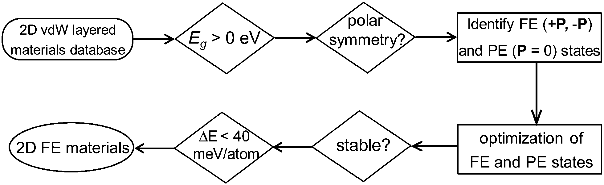 | ||
| Fig. 1 High-throughput screening scheme for 2D FE materials. We start by looking for non-metallic 2D monolayers without inversion symmetry, which restrict the search to about 260 types of 2D insulating or semiconducting monolayers with C1, C2, C2v, C3v, C4v and C6v polar point groups. We then analyze polarization for each candidate, and identify two potential FE states with opposite polarizations (±P states). The potential PE phase is obtained after “averaging” the atomic structures of the ±P states. After structural optimization, those 2D materials with unstable FE or PE structures are excluded. More importantly, the energy difference between the FE and PE phases (ΔE) should be small enough so that the polarization can be switchable. The energy criteria for ΔE is chosen to be 40 meV per atom, corresponding to the PE–FE energy difference in PbTiO3. Based on our material screening scheme, we not only obtain the known 2D FE materials, such as group-IV monochalcogenides, but also identify a new class of layered FE materials – NbOX2. | ||
Bulk NbOX2 have been synthesized since the 1960s,27,28 and they can be potentially exfoliated into 2D layered forms. Despite their structural polarities at room temperature,28–31 NbOX2 have not been considered or investigated as 2D layered ferroelectrics. Except for earlier tight-binding band structure calculations,32 accurate predictions regarding electronic and FE properties for NbOX2 bulk and 2D layers have never been reported. In our work, based on first-principles calculations, model Hamiltonian and molecular dynamics simulations, we identify the presence of stable FE and metastable antiferroelectric (AFE) phases in both 3D bulk and 2D layered forms of NbOX2. The coexistence of FE and AFE phases can lead to unique polarization switching and structural phase transition features in NbOX2, distinct from the currently known 2D FE materials. Our findings demonstrate NbOX2 as a practical system to study the intrinsic ferroelectricity and antiferroelectricity down to the monolayer limit, and to explore the novel functionalities associated with 2D FE/AFE phase transitions.
Results and discussion
Ground state structures and ferroelectric properties
Niobium oxide dihalides NbOCl2, NbOBr2 and NbOI2 belong to a group of transition metal oxide halide compounds with chemical formula MOX2 (M = V, Nb, Mo and Ta, and X = Cl, Br and I).27,28 Bulk NbOX2 is a typical van der Waals layered material,25 which is formed by stacking of NbOX2 monolayers along the out-of-plane direction. Due to the weak van der Waals interlayer interactions (the interlayer binding energy Eb = 12–13 meV Å−2 in Table 1, while the Eb of graphite is predicted to be 20.3 meV Å−2![[thin space (1/6-em)]](https://www.rsc.org/images/entities/char_2009.gif) 33), it should be eminently possible to obtain 2D NbOX2 multi-layers or monolayers via mechanical exfoliation techniques. Similar to the perovskite crystal structure, the NbOX2 monolayer is composed of NbO2X4 octahedra with mixed edge- and corner-sharing connectivity. Typically, as shown in Fig. 2(a), NbO2X4 octahedra build up a 2D structural network through extensive interconnecting X–X edges along one planar direction (crystallographic a axis) and cornered O atoms along the other (b axis).
33), it should be eminently possible to obtain 2D NbOX2 multi-layers or monolayers via mechanical exfoliation techniques. Similar to the perovskite crystal structure, the NbOX2 monolayer is composed of NbO2X4 octahedra with mixed edge- and corner-sharing connectivity. Typically, as shown in Fig. 2(a), NbO2X4 octahedra build up a 2D structural network through extensive interconnecting X–X edges along one planar direction (crystallographic a axis) and cornered O atoms along the other (b axis).
| NbOCl2 | NbOBr2 | NbOI2 | ||||
|---|---|---|---|---|---|---|
| Bulk | Monolayer | Bulk | Monolayer | Bulk | Monolayer | |
| E b (meV Å−2) | 12.19 | — | 12.77 | — | 13.40 | — |
| d Nb (Å) | 0.15 | 0.14 | 0.14 | 0.14 | 0.13 | 0.13 |
| ΔEFE (meV f.u.−1) | 13.31 | 13.63 | 10.64 | 11.00 | 8.12 | 9.08 |
| P (μC cm−2) | 26.86 | 26.50 | 22.28 | 22.32 | 17.78 | 17.66 |
| E g (eV) | 1.84 (3.73) | 1.88 (3.99) | 1.79 (3.07) | 1.87 (3.01) | 1.69 (1.83) | 1.77 (1.84) |
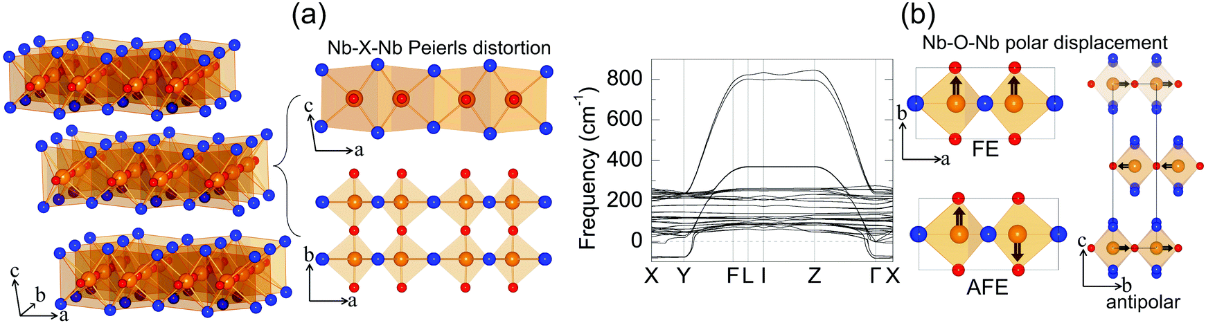 | ||
| Fig. 2 Layered structures of PE NbOX2. (a) Three-dimensional crystal structure for paraelectric (PE) phases of bulk NbOX2, with Nb in brown, O in red and halogen atoms X in blue. Both side and top views of an isolated PE NbOX2 monolayer are shown to highlight the one-dimensional Peierls distortion between neighboring Nb atoms along the crystallographic a axis. (b) Calculated phonon spectrum for bulk PE NbOI2. There are three unstable soft-phonon modes corresponding to FE, AFE and antipolar Nb polar displacement relative to the center of the NbO2I4 octahedra along the crystallographic b axis. The unit cell of NbOX2 is indicated by a black rectangle. | ||
As determined by experimental structural characterizations,29–31 bulk NbOX2 can crystalize in a ferroelectric C2 phase with monoclinic symmetry, where Nb cations exhibit non-zero off-center displacement along the Nb–O–Nb atomic chain direction (b axis). In our work, in order to explore all possible NbOX2 polar configurations, we choose the Nb polar-distortion free, centrosymmetric C2/m phase (ground state structures for MoOCl234 and TaOI235) as the paraelectric (PE) reference for bulk NbOX2. Fig. 2(a) displays the crystal structure for the PE bulk phase (crystallographic parameters shown in Table S1 of the ESI†), in which there exits one-dimensional Peierls distortion36 of Nb atoms in each NbO2X4 octahedra, leading to an alternation of two unequal Nb–Nb distances along the Nb–X–Nb direction (a axis). As we will discuss later, Nb–Nb Peierls distortion is crucial for determining the electronic structures and band gaps of NbOX2. After examining the phonon spectra of PE phases, the soft phonon modes and corresponding polar structural instabilities for bulk NbOX2 can be identified.
We use bulk NbOI2 as an example and display the calculated phonon spectrum of its PE phase in Fig. 2(b). Three types of soft optical phonon modes with imaginary frequencies at the Γ point (ω = i 83, 82 and 71 cm−1) are identified, corresponding to FE (all Nb atoms have exactly the same polar displacement), antipolar (two neighboring monolayers have anti-parallel Nb polar displacement) and AFE (Nb atoms from neighboring octahedra within each monolayer displace oppositely) Nb polar displacement patterns relative to the center of the NbO2I4 octahedra. It is noted that Nb polar displacement in all three modes is restricted along the Nb–O–Nb direction. We next inject each soft mode into PE NbOI2, followed by structural optimization to obtain lower symmetry polar phases. FE phases with C2 symmetry (Table S2 in the ESI†) are obtained after relaxation of FE-mode related structure. Cooperative displacement of all Nb atoms (polar displacement amplitude dNb ≈ 0.14 Å) in the FE phase can break inversion symmetry and generate non-zero spontaneous polarizations along the b axis, which can be qualified using Berry phase calculations. The typical polarization-energy double well curves are obtained for bulk NbOX2 FE phases (Fig. S1 in the ESI†), after recording the variation of polarization and total energy of the system with respect to the amplitude of the FE mode connecting the FE C2 and PE C2/m phases. Based on our calculations, bulk NbOCl2 exhibits the largest spontaneous polarization, highest FE potential depth and largest Nb polar displacement amplitude (Table 1), due to the significant electronegativity of the Cl anion. Besides the FE phase, antipolar phases with P2/c symmetry and AFE P![[1 with combining macron]](https://www.rsc.org/images/entities/char_0031_0304.gif) phases (crystallographic parameters shown in Tables S3 and S4 of the ESI†) with anti-parallel interlayer or intralayer Nb polar displacement are also identified. Each Nb cation in the antipolar or AFE phases has non-zero polar displacement, but their contributions to the overall polarization of the system cancel out.
phases (crystallographic parameters shown in Tables S3 and S4 of the ESI†) with anti-parallel interlayer or intralayer Nb polar displacement are also identified. Each Nb cation in the antipolar or AFE phases has non-zero polar displacement, but their contributions to the overall polarization of the system cancel out.
After investigation of bulk NbOX2, we now turn to 2D NbOX2 multi-layers and monolayers, where we will demonstrate these NbOX2 layers as intrinsic 2D FE (AFE) materials. The soft-mode adopted structural optimization scheme is also used to obtain the polar ground state structures for 2D NbOX2 layers. FE, antipolar and AFE soft modes are found in the PE phase of NbOX2 multi-layers, while the monolayers only have FE and AFE modes (Fig. S2 and Table S5 in the ESI†). Without a vertical stacking sequence and out-of-plane periodicity, all 2D NbOX2 layers are optimized into orthorhombic symmetry. Fig. 3(a) summarizes our calculated energetic results for all polar phases in NbOI2 (results for NbOCl2 and NbOBr2 are provided in Fig. S3 of the ESI†). The FE phase is the most stable structure for all NbOX2 layered systems, independent of the layer numbers. Except for the monolayer, the antipolar phase is the next most stable phase, and is very close to the FE phase in energy. Even the less stable AFE phase has a small energy difference (<2 meV f.u.−1) relative to the FE phase.
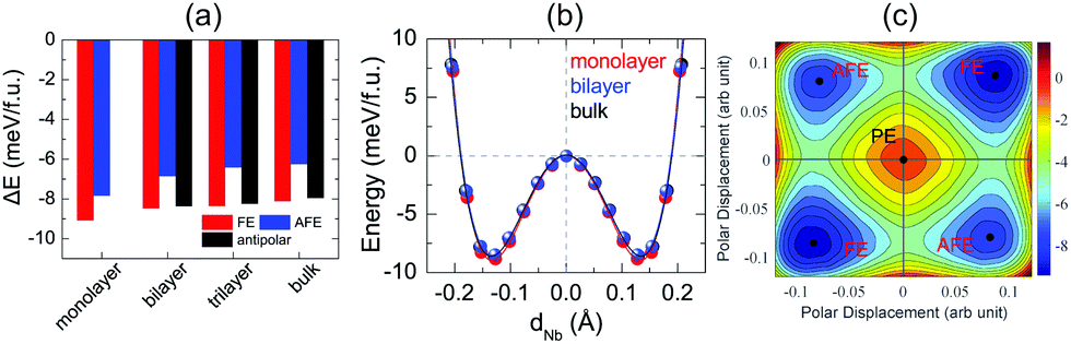 | ||
| Fig. 3 Energy profiles and FE polarization of 2D NbOI2 layers. (a) Variation of the total energy for different polar configurations in the NbOI2 system as a function of number of layers, where the energy of the corresponding PE phases are chosen as energy zero. The trend in the energy stability of different NbOI2 polar configurations is: FE ≈ antipolar > AFE. (b) Nb polar displacement-energy double well plots connecting PE and two FE phases in NbOI2 monolayer, bilayer and bulk. Symbols are the calculated results, lines are fitted to the data based on the Landau model. Both the magnitude of Nb polar displacement and FE potential depth remain almost unchanged with respect to the number of layers. (c) The calculated energy contour plot (in meV f.u.−1) of an isolated NbOI2 monolayer as a function of the polar displacement between two Nb atoms in one unit cell. One PE state and two energetically equivalent FE (AFE) states are identified. The energy of the PE state is set as the energy zero. | ||
FE phases of NbOX2 also show weak layer-dependent in-plane ferroelectricity due to the van der Waals interlayer interactions.37 Shown in Fig. 3(b) are the calculated double-well potential curves for FE NbOI2, where NbOI2 monolayer, bilayer and bulk exhibit almost identical Nb polar displacement amplitude and FE potential depth in their FE phases (similar results are also found in NbOCl2 and NbOBr2). Based on layer-independent energetic stability and ferroelectricity, it is expected that in-plane FE polarization of almost the same magnitude (Table 1) can be obtained in all structural forms of NbOX2, including 3D bulk and 2D layers. This unique feature makes 2D NbOX2 distinct from group-IV monochalcogenides (e.g. GeS, SnS and SnTe), a well studied 2D FE material class with in-plane ferroelectricity. As it is demonstrated by experiment, 2D orthorhombic SnTe layers (γ phase) exhibit strong antipolar interlayer coupling, leading to a vanishing of ferroelectricity in the bulk phase and those multi-layers containing even numbers of layers.16
NbOX2 monolayer can be stabilized into two polar phases, either a stable FE or metastable AFE phase, which contain two NbO2X4 octahedra in their unit cell. To evaluate the possibility of FE-to-AFE transition, we calculate 2D energy contour plot of NbOI2 monolayer as a function of polar displacement of two Nb atoms within a single unit cell. As shown in Fig. 3(c), two degenerate FE (AFE) phases locate along the diagonal directions, separated by the PE phase. Transition between two FE phases with opposite polarizations does not need to go through the high-energy PE phase. Instead, it will cross a low-lying AFE phase, where the polar displacement of one Nb atom is reversed, while keeping the other almost unchanged.
Electronic structure and optical absorption properties
Layered NbOX2, including 3D bulk and 2D layers, have FE ground states with spontaneous polarizations. The coupling between FE ordering and the electronic and optical properties of 2D materials can lead to interesting phenomena, such as the bulk photovoltaic9,38 and ferrovalley effects.12,39 We will investigate the electronic structures and optical absorption properties for the FE phases in bulk and monolayer NbOX2.Fig. 4 displays our calculated energy band structures and projected density of states (PDOS) for FE NbOX2, obtained from HSE hybrid density functional calculations. All NbOX2 systems, including 3D bulk and 2D monolayer, are predicted to be indirect semiconductors with nominal Eg (the energy difference between the filled and empty band edges, shown in Table 1) around 1.8 eV. Due to the hybridization of Nb-4d with anion p orbitals, largely dispersed energy bands around the conduction band minimum (CBM) in NbOX2 are mainly contributed to by empty Nb-4d states. Below the Fermi level, the highest occupied valence band is almost dispersionless through the entire Brillouin zones of the monoclinic bulk and orthorhombic monolayer. For NbOCl2 and NbOBr2, such a flat band is isolated from other valence bands of hybridized anion p orbitals. Further orbital component analysis indicates that the dispersionless valence bands (marked as green circles in the energy bands of the monolayers) originate from localized Nb-dz2 states. Meanwhile, similar weakly dispersed energy bands also appear in conduction states (above CBM), corresponding to empty Nb-dz2 orbitals.
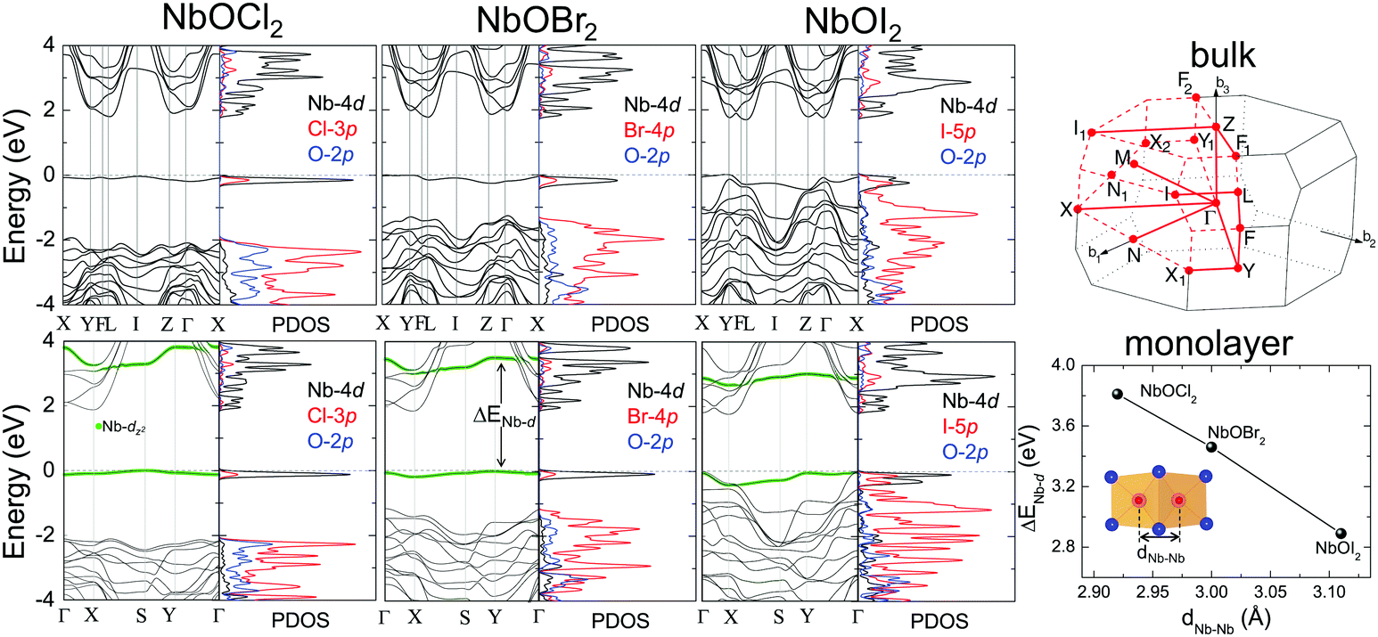 | ||
| Fig. 4 Electronic structures for FE NbOX2. HSE calculated energy band structures and projected density of states (PDOS) for FE bulk NbOX2 with C2 monoclinic symmetry (upper panel) and FE NbOX2 monolayer with Pmm2 orthorhombic symmetry (lower panel). Fermi energy level is set as energy zero. The choice of k-point path for the monoclinic Brillouin zone follows the convention from ref. 40. For NbOX2 monolayer, the contribution of Nb-dz2 orbital to energy bands are highlighted by green circles. The variation of the energy separation between the occupied and empty Nb-dz2 orbitals at Γ point (ΔENb-d) as a function of Nb–Nb paring distance (dNb–Nb) in FE NbOX2 monolayers is also presented. NbOCl2 monolayer with the shortest dNb–Nb has the strongest Peierls distortion intensity and therefore the largest ΔENb-d. | ||
Formation of the energy gap between the filled and empty Nb-dz2 states (ΔENb-d) is a direct consequence of 1D Peierls distortion.36 Each Nb4+ cation in NbOX2 has one unpaired 4d electron. Paring of two 4d electrons simultaneously occurs in the NbOX2 single unit cell, after periodic dimerization of neighboring Nb cations created by the 1D Peierls distortion. The energy gap is then formed as two paired electrons are favored to fully occupy the low-energy Nb-dz2 orbital, leaving the high-energy dz2 orbital empty. We double checked the electronic structures for NbOX2 using spin polarized calculations, which also predict nonmagnetic ground states with paired electrons on the Nb-dz2 orbitals. In fact, the intensity of the 1D Peierls distortion in NbOX2 can be well qualified by energy separation between the occupied and empty Nb-dz2 orbitals (ΔENb-d). As shown in the last plot of Fig. 4, the strongest Peierls distortion with the shortest Nb–Nb distance in NbOCl2 monolayer leads to the largest ΔENb-d. The overall extraordinarily large ΔENb-d in all three systems indicates that 1D Peierls distortion in NbOX2 is ultra-stable, able to survive over thermal fluctuations at high temperature.
In layered NbOX2, Nb-dz2 orbitals can hardly hybridize with any planar anion p orbitals. As a result, Nb-dz2 states correspond to the dispersionless energy bands that are quite localized in energy. More importantly, optical transitions from the localized Nb-dz2 valence band to other empty Nb-d orbitals from conduction bands are completely forbidden. The effective optical absorption in NbOX2 comes from the transition between hybridized anion-p orbitals of the valence band and hybridized Nb-4d orbitals (except dz2) of the conduction bands. Therefore, as far as optical absorption properties are considered, NbOCl2 and NbOBr2 are insulators with optical transition allowed Eg > 3.0 eV (Table 1). Due to the weak electronegativity of the I anion, bulk and monolayer NbOI2 can exhibit semiconducting electronic and optical properties. Typically, as a ferroelectric semiconductor with an indirect Eg, bulk NbOI2 can effectively absorb visible light with a photon energy above 2.0 eV (Fig. S4 in the ESI†), making it suitable for FE photovoltaic applications.41,42
2D NbOX2 layers have orthorhombic symmetry with anisotropic planar crystal structures, where Nb atoms bond with X–X edges along one planar direction and O atoms along the other. Similarly to many other 2D FE materials,12,43 strong anisotropy in crystal structures of 2D NbOX2 will be reflected in their energy bands and optical absorption properties as well. Using semiconducting monolayer NbOI2 as an example, we will illustrate its highly anisotropic and strongly coupled electronic and optical absorption properties. Fig. 4(a) shows the band structure for FE NbOI2 monolayer, where all the energy bands around the Fermi energy level are marked by colored circles whose radii are proportional to the contribution of the corresponding atomic orbitals. I anion has a weaker electronegativity than O, therefore the valence bands around the Fermi level mainly come from I-p orbitals. Except for the localized dz2 bands, most valence and conduction bands show anisotropic dispersion along two planar directions: valence I-py bands and low-lying conduction Nb-dyz bands are highly dispersed along Γ–Y (reciprocal lattice equivalent of the crystallographic b axis), but weakly dispersed along the Γ–X direction.
Besides electronic structures, we have also investigated the anisotropic optical properties of NbOI2 monolayer by simulating its optical absorption coefficient α, excited by incident light polarized along the x and y directions (corresponding to the a and b axes, respectively). As shown in Fig. 5(b), both αx and αy have optical absorption edges around 2.0 eV. Above the absorption edge, a strong optical absorption peak appears at 3.15 eV, when incident light is polarized along the x direction. The strength of this absorption peak in αx is larger than that of αy by almost 10 times, indicating a strong direction-dependent photo-absorption in NbOI2 monolayer. As energy bands around the Fermi level are mainly contributed to by hybridized I-p and Nb-d orbitals, the low-energy optical absorption in NbOI2 can be assigned to optical transitions from I-p to Nb-d orbitals. When NbOI2 monolayer is excited by incident light polarized along the x direction, optical transitions between all weakly dispersed Nb-dyz and I-py energy bands along the whole Γ–X direction (indicated by dashed red arrows in Fig. 5(a)) can contribute to optical absorption at 3.15 eV in αx. While along the y direction, the weaker absorption at 3.15 eV comes from the optical transition (blue dashed arrow) of Nb-dyz and I-py bands around the Γ point only. As a result, when monochromatic light with photon energy of 3.15 eV is incident on FE NbOI2 monolayer, optical absorption along the nonpolar a axis is significantly larger than that along the polar axis, leading to a nearly linearly polarized optical absorption selectivity in NbOI2 monolayer.39
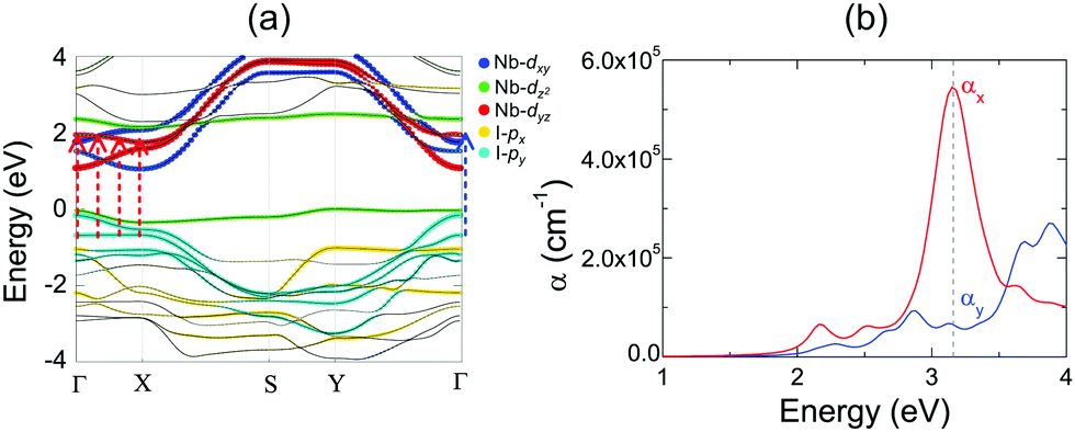 | ||
| Fig. 5 Anisotropic electronic structure and optical absorptions of NbOI2 monolayer. (a) Calculated band structure for FE NbOI2 monolayer. The radii of the colored circles are proportional to the contribution of the corresponding atomic orbitals. The Fermi energy level is set as energy zero. (b) The optical absorption spectrum for FE NbOI2 monolayer under incident light polarized along crystallographic a and b axes (x and y directions), respectively. Blue and red arrows in (a) indicate the optical transitions that contribute to the anisotropic optical absorption peaks around 3.15 eV, which are marked by the dashed line in (b). | ||
Ferroelectric polarization switching and domain-wall properties
It is clearly shown that layered NbOX2 systems have in-plane ferroelectricity at the monolayer limit. As a fundamental nature of ferroelectricity, FE polarizations in 2D NbOX2 should be switchable under an applied electric field. Unlike other 2D FE materials with planar ferroelectricity (e.g. SnS and SnSe), FE ordering in 2D NbOX2 monolayers indeed has a “1D” nature, as the ferroelectricity or antiferroelectricity is restricted along the polar b axis, but forbidden along the other nonpolar axis. Based on its 1D collinear nature, FE polarization switching in 2D NbOX2 monolayers can be achieved through the direct reversal of the polarization direction by 180°, rather than rotation of polarization across the nonpolar axis.During the polarization reversal (switching) process, FE domain-walls between oppositely orientated FE mono-domains will be formed in NbOX2 monolayers. Meanwhile, the polarization reversal process can be carried out through the motion of FE domain-walls.44,45Fig. 6(a) displays the supercell configuration containing two FE mono-domains with opposite polarization directions, separated by a 180° FE domain-wall located along the I–I lattice plane in NbOI2 monolayer. Each mono-domain is composed of four NbOI2 unit cells, stacking along the a axis. To preserve the periodic boundary condition required by first-principles plane wave calculations, we must include two coherent FE domain-walls (twin walls) in one supercell, so that the whole supercell can be repeated periodically along both axes.
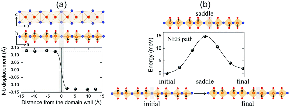 | ||
| Fig. 6 FE domain wall and polarization reversal process. (a) Atomic structure (including side and top views) for a 180° FE domain-wall (marked by the grey area) between two oppositely oriented FE mono-domains in NbOI2 monolayer. The change of the associated Nb polar displacement as a function of the distance from the domain-wall is also given. Symbols are the calculated results, the solid line is fitted to the data based on domain wall theory and the dashed lines indicate the mono-domain values. (b) Minimum energy pathway (MEP) for polarization reversal and the associated domain wall motion process obtained from solid-state NEB calculations. Reversal of NbOI2 polarization is achieved by motion of the FE domain wall from one I–I lattice plane to the next. Atomic structures for initial, saddle and final states along the simulated MEP are also presented. Black arrows indicate the polar displacement of Nb cations. All calculations were performed using the supercell configuration containing eight NbOI2 unit cells. For clarity, only half of the domain-wall supercell is shown. | ||
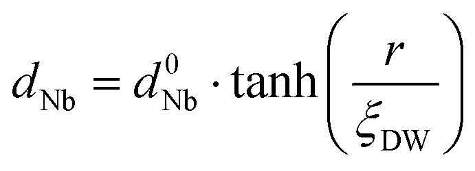
In order to evaluate how polarization is reversed across the FE domain-wall, we analyze the evolution of Nb polar displacement amplitude (dNb) as a function of Nb distance (r) away from the domain-wall. As shown in Fig. 6(a), polarization is reversed as dNb changes its sign abruptly across the domain-wall. dNb of each Nb cation almost fully recovers to its mono-domain value (indicated by dashed lines). As a result, the 180° FE domain-wall supercell configuration is geometrically similar to a NbOI2 superlattice, where AFE phases are sandwiched between two FE phases with opposite polarizations. As the energy difference between AFE and FE phases of NbOI2 monolayer is as low as 1.24 meV f.u.−1, the 180° FE domain-wall has a very small domain wall energy. The dNb–r curve shown in Fig. 6(a) can be quantitatively described using a function corresponding to the soliton solution of one-dimensional fourth-order Landau–Ginzburg domain wall theory44 as:
 | (1) |
We then explore the kinetic process for domain-wall motion by simulating the corresponding minimum energy pathway (MEP) trajectory and the associated energy barrier height, using a generalized solid-state NEB method.46 Such a method allows both atomic positions and lattice parameters to relax along the pathway. As shown in Fig. 6(b), transition from the initial to the final domain-wall configurations resembles the motion of the domain wall from one I–I lattice plane to the next, accompanied by the reversal of polarization direction of one group of Nb cations by 180°. At the saddle point configuration along the MEP, the domain-wall moves to the lattice plane where Nb cation is located. This very Nb cation is then constrained to have zero dNb, while dNb of other Nb cations remain unchanged. As a result, the MEP associated with domain-wall motion is similar to the energy pathway for transition from single FE to AFE phase, as we obtained earlier from the energy contour plot in Fig. 3(c). The overall barrier height for polarization reversal of the Nb cation in the NbOI2 monolayer is predicted to be 14.9 meV, which is much smaller than the polarization rotation barrier (∼40 meV) in FE perovskite PbTiO3.47 Therefore, the presence of the low-lying AFE phase can lead to a small energy barrier, which is beneficial for easy domain-wall motion and polarization switching in NbOI2 monolayer.
Using the simulated energy barrier, we can estimate how large the electric field needs to reverse FE polarization in NbOI2 monolayer. The critical electric field EC is given by: EC ≃ Ebarrier/P·V, where P is the spontaneous polarization and V is the normalized cell volume for NbOI2 monolayer. The estimated critical electric field EC ≃ 0.63 MV cm−1, which is readily accessible by experiment.48 Therefore, electric field induced switching of FE polarization can be achievable under laboratory conditions.
Structural phase transition at finite temperature
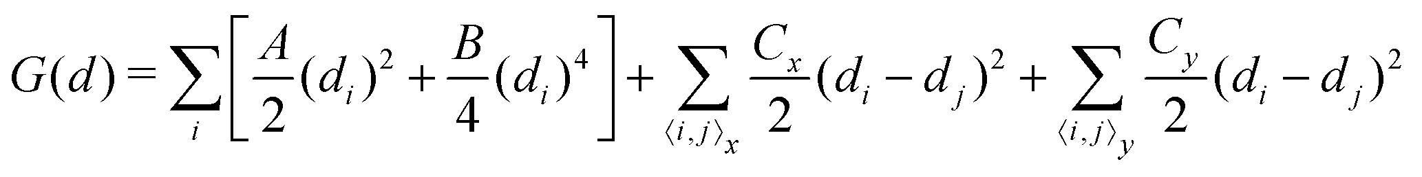
Up to now, we have simulated the structural, electronic and polarization switching properties for FE NbOX2 layers using zero-temperature DFT calculations. For practical applications of ferroelectrics, 2D NbOX2 should have relatively high Curie temperature TC, so that their polarizations can still persist above room temperature. In the following, we will investigate the ferroelectricity and structural phase-transition of NbOX2 monolayers at finite temperature using both Monte Carlo (MC) and ab initio molecular dynamics (MD) simulations.The geometry of 2D NbOX2 monolayers can be represented by a 2D lattice grid containing a number of Nb cations, where each Nb cation at 2D grid point i [i is a collapsed index of its 2D position (m, n)] has a unique polar displacement di. Due to the 1D nature of polarization, di of Nb cations are collinearly arranged into columns along the polar axis. Using polar displacement di as the order parameter, the configuration of NbOX2 monolayer at any condition can be unambiguously specified. Therefore, we can express the free energy of NbOX2 monolayer as Landau–Ginzburg expansion of order parameter di as:13
 | (2) |
| A | B | C x | C y | T C (K) | |
|---|---|---|---|---|---|
| NbOCl2 | −1.29 × 10³ | 3.03 × 10⁴ | 48.23 | 6.08 × 10³ | 396 |
| NbOBr2 | −1.11 × 10³ | 2.74 × 10⁴ | 38.68 | 4.28 × 10³ | 283 |
| NbOI2 | −1.01 × 10³ | 2.85 × 10⁴ | 19.14 | 4.82 × 10³ | 242 |
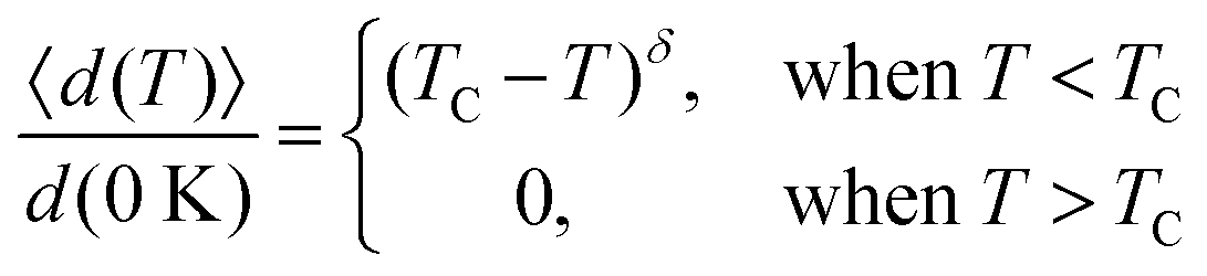
Based on the effective Hamiltonian we developed for NbOX2 monolayers, we can investigate temperature induced structural transition using MC simulations (computational details in the ESI†). For comparison, we also perform parameter-free ab initio MD simulations, where the time evolution of the instantaneous temperature, total energies and cation polar displacement of NbOX2 can be obtained (Fig. S6 in the ESI†). Due to the large computational cost, we restrict our MD simulations of NbOX2 monolayers to selected target temperature. Fig. 7 shows our simulated temperature dependent macroscopic average polar displacement 〈d(T)〉 in NbOX2 monolayers. The structural transition from FE to PE phase is identified, as the simulated 〈d(T)〉 drops abruptly to zero around TC. Moreover, at the selected temperature, ab initio MD predicted ensemble average 〈d(T)〉 are in overall good agreement with MC results (the largest derivation occurs in NbOI2, with ΔT ∼ 60 K), which validates the effective Hamiltonian and parameters we used for MC simulations. Curie temperature TC can be quantitatively determined after fitting MC simulated 〈d(T)〉 as follows:13
 | (3) |
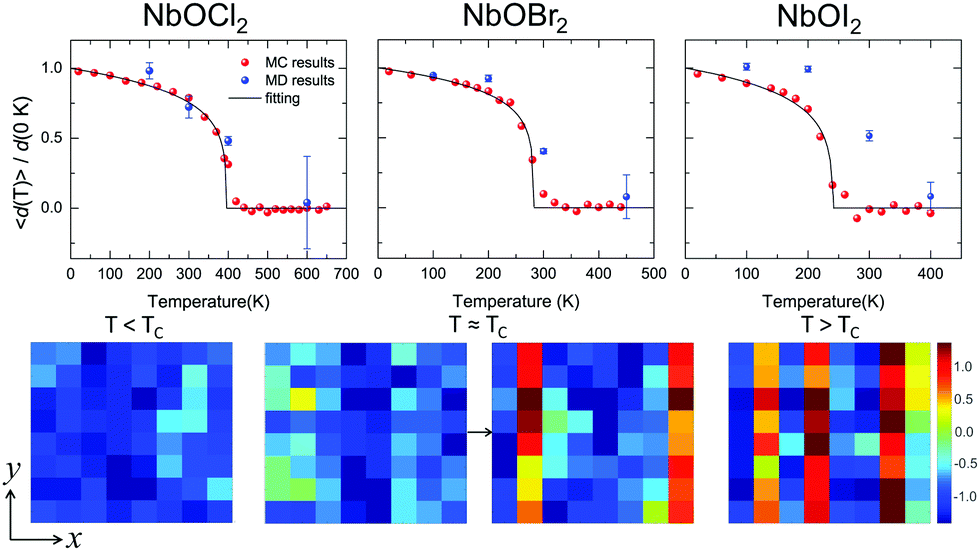 | ||
| Fig. 7 Structural phase-transitions and Curie temperatures of NbOX2 monolayers. Upper panel: Temperature dependence of the average Nb polar displacement obtained from MC and ab initio MD simulations for NbOCl2, NbOBr2 and NbOI2 monolayers. Average polar displacement 〈d(T)〉 is normalized with respect to the corresponding 0 K value. Black lines are fitted to MC data based on eqn (3). The error bars of Nb polar displacement highlight the thermal fluctuations during the MD simulations. Lower panel: MD simulated polarization reversal process in NbOI2 monolayer. The normalized polar displacements (di(T)/|d(0 K)|) for each Nb cation in a 8 × 8 lattice grid are presented when the temperature is below, approaching and above Curie temperature TC. Polarization reversal occurs when T ≈ TC, and is initiated by switching di of a single Nb from one cation column along the polar axis (y direction). | ||
In order to understand the microscopic mechanism governing FE–PE phase transition, we further examine temperature dependent cation displacement evolution. The lower panel of Fig. 7 plots the real space mapping of di from the whole NbOI2 lattice grid during MD simulations after the system reaches thermal equilibrium at target temperature below, approaching and above TC, respectively. Below TC, the magnitude of di starts to decrease from its zero temperature value as temperature increases. The polarization reversal event (changing sign of di) does not occur until T ≈ TC, where |di| of some Nb cations become small enough so that thermal energy is comparable with the energy cost to form a head-to-head/tail-to-tail polar configuration. The polarization reversal process around TC is initiated by switching di of a single Nb cation from one cation column. Then the whole column simultaneously switches its polarization to the opposite direction, to avoid the unfavorable head-to-head/tail-to-tail configuration. The FE–PE phase transition is achieved through dynamic reversal of column polarization as mentioned above. As AFE phase in NbOX2 is more stable than the distortion-free PE phase. Even when T > TC, the system stays in a thermal-equilibrium PE state, where the overall polarization is almost zero, but individual columns can still have non-zero and randomly oriented polarization along the polar axis. As a result, PE state above TC is more like a disordered AFE phase. Moreover, the energy cost associated with “collective” reversal of whole column polarization is negligible compared to the “isolated” cation dipole switching energy (Cy ≫ Cx, Table 2), thus TC of NbOX2 monolayer is mainly determined by “isolated” rather than “collective” cation dipole switching events.49 Therefore, TC is not simply proportional to the energy difference associated with “collective” polarization reversal (FE-to-AFE phase transition). Even though AFE phase is close to FE phase in energy, NbOX2 monolayers can still have TC around or even above room temperature.
Experimental outlook and FE device by design
We have provided strong evidence that 2D NbOX2 possess intrinsic in-plane ferroelectricity and antiferroelectricity. Experimentally, bulk NbOX2 have already been prepared using solid-state sintering methods, while their structure polarity at room temperature was verified by XRD measurement.28–31 Direct identification of ferroelectricity or antiferroelectricity in bulk NbOX2 requires further measurement of their polarization–electric field (P–E) hysteresis loops. 2D NbOX2 layers, including multilayers and monolayers can be obtained by direct exfoliation of bulk samples or chemical vapor deposition. As long as the temperature is below TC, 2D NbOX2 layers can crystalize in a ground state FE phase with polarization comparable with that of bulk NbOX2, after poling by electric field (above critical field EC) applied along the polar axis. Based on our simulation, 2D NbOX2 monolayers exhibit variable FE polarizations and TC. Chemical alloys made of individual NbOX2 end members can offer a wide range of material choice to achieve optimal TC and FE properties. For example, a 2D NbOClxI2−x monolayer is expected to possess TC above room temperature and semiconducting properties comparable with NbOI2. More specifically, increasing concentration x can lead to a higher TC and larger optical transition allowed Eg in the NbOClxI2−x monolayer. Alternatively, one can also use experimentally accessible tensile strain to engineer the FE properties of NbOX2 monolayers. As shown in Fig. S7 of the ESI,† more than 6 times enhancement of the FE potential depth and twice of the Nb polar displacement can be achieved with 3% tensile strain applied along the polar axis of NbOX2 monolayers. As a result, tensile strained NbOBr2 and NbOI2 monolayers are expected to have elevated TC above room temperature. Due to linearly polarized optical selectivity of the semiconducting NbOI2 monolayer, its in-plane polar and non-polar axes can be easily distinguished using incident polarized light. As NbOX2 have the interconnected octahedral structural framework similar to perovskite oxides, after imaging of Nb off-center polar displacement (0.13–0.14 Å) using annular bright-field scanning transmission electron microscopy (ABF-STEM),50,51 one can directly observe and quantify FE polarization appearing in 2D NbOX2 layers. Moreover, measuring the shear piezoelectric effect arising from in-plane polarization by lateral piezoelectric force microscopy (PFM)37 can also provide a direct experimental proof of FE polarization in 2D NbOX2.The 1D polarization nature and coexistence of FE/AFE phases make 2D NbOX2 exhibit the unique polarization reversal and structural phase-transition features. In experiment, AFE perovskite oxides have been widely used as dielectric capacitors for electrostatic energy storage through electric charging and discharging processes.52 In particular, high energy densities are achieved in perovskite solid solutions near the phase boundaries where FE and AFE phases coexist.53 We therefore propose the application of NbOX2 monolayers as 2D dielectric capacitors.
Fig. 8(a) displays a schematic diagram for a 2D single-layered capacitor obtained by lateral growth of a heterostructure between a NbOX2 monolayer and another 2D metallic material, where an electric field can be applied along the polar axis through a metal electrode. In order to evaluate the performance of a 2D NbOX2 based capacitor, we choose NbOI2 monolayer as an example, and investigate the electric-field induced phase transition by simulating its P–E loop around room temperature using MC simulations. When electric field E is applied along the polar axis, the additional energy term −(E·P)V will be incorporated into the effective Hamiltonian in eqn (2). The effective polarization P can be computed from Nb polar displacement di and Born effective charge Zi* by: 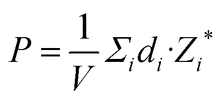 . Therefore, the electric field related energy term can be simplified as: −E(Σidi·Zi*). Based on our predictions, NbOI2 monolayer adopts a disordered AFE (PE) phase at room temperature. The simulated P–E loop in Fig. 8(b) shows that under the charging process (increasing E) P increases abruptly around 0.15 MV cm−1, indicating that a small critical field EC can trigger the AFE-to-FE transition in NbOI2 monolayer at room temperature. Above EC, P increases linearly within FE phase upon further charging. Remarkably, an almost identical P–E curve associated with the FE-to-AFE transition is obtained under the discharging process (decreasing E). As a result, under the applied electric field, NbOI2 monolayer possesses P–E loops with almost no hysteresis, which is consistent with its small FE/AFE energy difference and low polarization switching energy barrier at room temperature.54 Similarly to NbOI2, NbOBr2 monolayer also crystalizes in a disordered AFE phase at room temperature and exhibits nearly hysteresis-free P–E loops. While NbOCl2 monolayer has a non-zero FE polarization at room temperature, it features P–E double hysteresis loops of typical ferroelectrics. Due to the energy loss associated with the hysteresis, NbOCl2 monolayer is less suitable for electrostatic energy storage than NbOBr2 or NbOI2. A 2D capacitor based on NbOBr2 or NbOI2 monolayers can exhibit nearly zero energy loss during the charging and discharging processes, yet has the advantage of operating at a low electric field, which can potentially enable nearly 100% efficiency for electrostatic energy storage in the 2D monolayer.
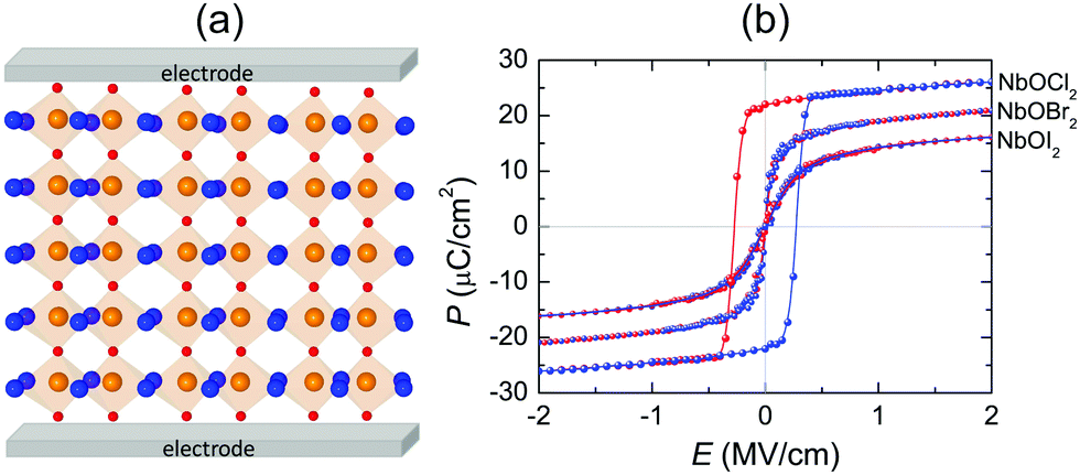 | ||
| Fig. 8 Electrostatic energy storage in a 2D FE capacitor. (a) Schematic model for a 2D FE capacitor device based on NbOX2 monolayers. (b) MC simulated P–E loops for NbOX2 monolayers at room temperature. Electric field E is applied along the polar axis. Results corresponding to the electric charging and discharging processes are marked in red and blue colors, respectively. | ||
Conclusions
In summary, we have identified niobium oxide dihalides NbOX2 as a new family of 2D van der Waals layered materials, exhibiting intrinsic in-plane ferroelectricity and antiferroelectricity. Comprehensive investigations regarding structural, ferroelectric, electronic, optical absorption and domain-wall properties of 2D NbOX2 have been carried out using first-principles calculations. NbOX2 adopts a 2D structural framework composed of interconnected NbO2X4 octahedra, where considerable cation off-center polar displacement along one planar axis can lead to 1D ferroelectricity or antiferroelectricity. Along the other planar axis, the ultra-stable Peierls distortion between Nb4+ cations gives rise to the semiconducting or insulating electronic properties, which are preferable for stable polarizations. In-plane ferroelectricity or antiferroelectricity in 2D NbOX2 can be sustained down to the monolayer limit, and the energetic stabilities and polar magnitudes are almost independent of the number of layers. Coexistence of FE and AFE phases makes 2D NbOX2 exhibit easily switchable polarizations. Moreover, the strong coupling between FE order and optical absorption leads to a nearly linearly polarized optical selectivity in the semiconducting NbOI2 monolayer. Besides zero temperature DFT calculations, we also develop an effective Hamiltonian to simulate the structural phase transitions of NbOX2 monolayers under finite temperature and an applied electric field. The NbOCl2 monolayer is predicted to be a robust FE material with room temperature stable ferroelectricity, while NbOBr2 and NbOI2 monolayers adopt a PE state composed of disordered AFE phases at room temperature, but will undergo a structural transition into a stable FE phase under a small applied electric field. Based on our simulations, P–E loops characterizing AFE–FE transitions have nearly zero hysteresis, therefore a capacitor composed of NbOBr2 or NbOI2 has a great advantage for highly efficient electrostatic energy storage. We hope our work will motivate future experimental exploration of 2D ferroelectricity and antiferroelectricity in layered NbOX2, and realization of superior energy storage performance that our simulations predicted.Computational methods
Our first-principles calculations are performed based on density functional theory (DFT) as implemented in the Vienna ab initio Simulation Package (VASP-5.4.1).55,56 A plane-wave basis set within the projector augmented-wave method57 is employed, using a 600 eV plane-wave energy cutoff. We simulate NbOX2 bulk and 2D layered structures using the strongly constrained and appropriately normed (SCAN) meta-GGA functional.58 After inclusion of the revised Vydrov–van Voorhis nonlocal correlation (rVV10),33,59 SCAN + rVV10 functional can accurately predict the interlayer spacings as well as intralayer lattice parameters for bulk NbOX2 (Table S2 in the ESI†). 2D NbOX2 layers are modeled as slabs with a vacuum region of more than 20 Å along the out-of-plane direction. A Γ-centered Monkhorst–Pack k-point grid of about 40 k-points per Å−1 spacing is used for k-point sampling. NbOX2 bulk and layers are fully optimized until the residual Hellmann–Feynman forces are smaller than 1 meV Å−1 and the stresses less than 0.1 kbar. Phonon frequencies and eigenvectors are calculated based on the finite difference method implemented in the Phonopy package.60 The electronic structures and optical absorption spectra of NbOX2 systems are further calculated using the Heyd–Scuseria–Ernzerhof (HSE06) hybrid functional.61,62 As band gap changes due to spin–orbital coupling (SOC) effects are quite small (ΔEg < 0.02 eV for bulk NbOI2), the SOC effect is excluded during HSE calculations. The electronic contribution to the polarization is calculated following the Berry phase formalism.63 The generalized solid-state nudged elastic band (ss-NEB) method46,64,65 is used to simulate the minimum energy path (MEP) and associated energy barriers for various kinetic processes.Conflicts of interest
There are no conflicts to declare.Acknowledgements
Work in XJTU is supported by funding from the National Science Foundation of China under Contract No. 11574244, 51320105014 and 51621063, the State Key Laboratory for Mechanical Behavior of Materials, as well as computational support from the National supercomputer center (NSCC) in Tianjin. X. C. Z. is supported by the National Science Foundation (NSF) through the Nebraska Materials Research Science and Engineering Center (MRSEC) (Grant No. DMR-1420645), and UNL Holland Computing Center. Y. J. thanks Dr Liang Ma, Dr Chongqin Zhu, Dr Ruixiang Fei and Prof. Yunhao Lu for helpful discussions.References
- M. Dawber, K. M. Rabe and J. F. Scott, Rev. Mod. Phys., 2005, 77, 1083–1130 CrossRef CAS.
- A. Belianinov, Q. He, A. Dziaugys, P. Maksymovych, E. Eliseev, A. Borisevich, A. Morozovska, J. Banys, Y. Vysochanskii and S. V. Kalinin, Nano Lett., 2015, 15, 3808–3814 CrossRef CAS PubMed.
- F. Liu, L. You, K. L. Seyler, X. Li, P. Yu, J. Lin, X. Wang, J. Zhou, H. Wang, H. He, S. T. Pantelides, W. Zhou, P. Sharma, X. Xu, P. M. Ajayan, J. Wang and Z. Liu, Nat. Commun., 2016, 7, 12357 CrossRef CAS PubMed.
- L. Niu, F. Liu, Q. Zeng, X. Zhu, Y. Wang, P. Yu, J. Shi, J. Lin, J. Zhou, Q. Fu, W. Zhou, T. Yu, X. Liu and Z. Liu, Nano Energy, 2019, 58, 596–603 CrossRef CAS.
- J. Junquera and P. Ghosez, Nature, 2003, 422, 506–509 CrossRef CAS PubMed.
- D. D. Fong, G. B. Stephenson, S. K. Streiffer, J. A. Eastman, O. Auciello, P. H. Fuoss and C. Thompson, Science, 2004, 304, 1650–1653 CrossRef CAS PubMed.
- J. Feng, X. Qian, C.-W. Huang and J. Li, Nat. Photonics, 2012, 6, 866–872 CrossRef CAS.
- A. Castellanos-Gomez, R. Roldán, E. Cappelluti, M. Buscema, F. Guinea, H. S. J. van der Zant and G. A. Steele, Nano Lett., 2013, 13, 5361–5366 CrossRef CAS PubMed.
- T. Rangel, B. M. Fregoso, B. S. Mendoza, T. Morimoto, J. E. Moore and J. B. Neaton, Phys. Rev. Lett., 2017, 119, 067402 CrossRef PubMed.
- P. Luo, F. Zhuge, Q. Zhang, Y. Chen, L. Lv, Y. Huang, H. Li and T. Zhai, Nanoscale Horiz., 2019, 4, 26–51 RSC.
- M. Wu and X. C. Zeng, Nano Lett., 2016, 16, 3236–3241 CrossRef CAS PubMed.
- H. Wang and X. Qian, 2D Mater., 2017, 4, 015042 CrossRef.
- R. Fei, W. Kang and L. Yang, Phys. Rev. Lett., 2016, 117, 097601 CrossRef PubMed.
- M. Mehboudi, B. M. Fregoso, Y. Yang, W. Zhu, A. van der Zande, J. Ferrer, L. Bellaiche, P. Kumar and S. Barraza-Lopez, Phys. Rev. Lett., 2016, 117, 246802 CrossRef PubMed.
- K. Chang, J. Liu, H. Lin, N. Wang, K. Zhao, A. Zhang, F. Jin, Y. Zhong, X. Hu, W. Duan, Q. Zhang, L. Fu, Q.-K. Xue, X. Chen and S.-H. Ji, Science, 2016, 353, 274–278 CrossRef CAS PubMed.
- K. Chang, T. P. Kaloni, H. Lin, A. Bedoya-Pinto, A. K. Pandeya, I. Kostanovskiy, K. Zhao, Y. Zhong, X. Hu, Q.-K. Xue, X. Chen, S.-H. Ji, S. Barraza-Lopez and S. S. P. Parkin, Adv. Mater., 2018, 31, 1804428 CrossRef PubMed.
- W. Ding, J. Zhu, Z. Wang, Y. Gao, D. Xiao, Y. Gu, Z. Zhang and W. Zhu, Nat. Commun., 2017, 8, 14956 CrossRef CAS PubMed.
- Y. Zhou, D. Wu, Y. Zhu, Y. Cho, Q. He, X. Yang, K. Herrera, Z. Chu, Y. Han, M. C. Downer, H. Peng and K. Lai, Nano Lett., 2017, 17, 5508–5513 CrossRef CAS PubMed.
- C. Cui, W.-J. Hu, X. Yan, C. Addiego, W. Gao, Y. Wang, Z. Wang, L. Li, Y. Cheng, P. Li, X. Zhang, H. N. Alshareef, T. Wu, W. Zhu, X. Pan and L.-J. Li, Nano Lett., 2018, 18, 1253–1258 CrossRef CAS PubMed.
- J. Xiao, H. Zhu, Y. Wang, W. Feng, Y. Hu, A. Dasgupta, Y. Han, Y. Wang, D. A. Muller, L. W. Martin, P. Hu and X. Zhang, Phys. Rev. Lett., 2018, 120, 227601 CrossRef CAS PubMed.
- S. Wan, Y. Li, W. Li, X. Mao, W. Zhu and H. Zeng, Nanoscale, 2018, 10, 14885–14892 RSC.
- F. Xue, W. Hu, K.-C. Lee, L.-S. Lu, J. Zhang, H.-L. Tang, A. Han, W.-T. Hsu, S. Tu, W.-H. Chang, C.-H. Lien, J.-H. He, Z. Zhang, L.-J. Li and X. Zhang, Adv. Funct. Mater., 2018, 28, 1803738 CrossRef.
- S. N. Shirodkar and U. V. Waghmare, Phys. Rev. Lett., 2014, 112, 157601 CrossRef PubMed.
- Y. Fang, X. Hu, W. Zhao, J. Pan, D. Wang, K. Bu, Y. Mao, S. Chu, P. Liu, T. Zhai and F. Huang, J. Am. Chem. Soc., 2019, 141, 790–793 CrossRef CAS PubMed.
- G. Cheon, K.-A. N. Duerloo, A. D. Sendek, C. Porter, Y. Chen and E. J. Reed, Nano Lett., 2017, 17, 1915–1923 CrossRef CAS PubMed.
- N. Mounet, M. Gibertini, P. Schwaller, D. Campi, A. Merkys, A. Marrazzo, T. Sohier, I. E. Castelli, A. Cepellotti, G. Pizzi and N. Marzari, Nat. Nanotechnol., 2018, 13, 246 CrossRef CAS PubMed.
- H. Schnering and H. Wöhrle, Angew. Chem., 1963, 75, 684 CrossRef.
- H. Hillebrecht, P. Schmidt, H. Rotter, G. Thiele, P. Zönnchen, H. Bengel, H.-J. Cantow, S. Magonov and M.-H. Whangbo, J. Alloys Compd., 1997, 246, 70–79 CrossRef CAS.
- D. Drobot and E. Pisarev, Russ. J. Inorg. Chem., 1984, 29, 1561–1563 Search PubMed.
- J. Beck and C. Kusterer, Z. Anorg. Allg. Chem., 2006, 632, 2193–2194 CrossRef CAS.
- J. Rijnsdorp and F. Jellinek, J. Less-Common Met., 1978, 61, 79–82 CrossRef CAS.
- M.-H. Whangbo, Inorg. Chem., 1982, 21, 1721–1723 CrossRef CAS.
- H. Peng, Z.-H. Yang, J. P. Perdew and J. Sun, Phys. Rev. X, 2016, 6, 041005 Search PubMed.
- P. Zonnchen, G. Thiele, C. Hess, C. Schlenker, H. Bengel, H. Cantow, S. Magonov, D. Seo and M. Whangbo, New J. Chem., 1996, 20, 295–300 Search PubMed.
- M. Ruck, Acta Crystallogr., Sect. C: Cryst. Struct. Commun., 1995, 51, 1960–1962 CrossRef.
- S. van Smaalen, Acta Crystallogr., Sect. A: Found. Crystallogr., 2004, 61, 51–61 CrossRef PubMed.
- L. You, F. Liu, H. Li, Y. Hu, S. Zhou, L. Chang, Y. Zhou, Q. Fu, G. Yuan, S. Dong, H. Fan, A. Gruverman, Z. Liu and J. Wang, Adv. Mater., 2018, 30, 1803249 CrossRef PubMed.
- S. M. Young and A. M. Rappe, Phys. Rev. Lett., 2012, 109, 116601 CrossRef PubMed.
- X.-W. Shen, W.-Y. Tong, S.-J. Gong and C.-G. Duan, 2D Mater., 2018, 5, 011001 CrossRef.
- W. Setyawan and S. Curtarolo, Comput. Mater. Sci., 2010, 49, 299–312 CrossRef.
- I. Grinberg, D. V. West, M. Torres, G. Gou, D. M. Stein, L. Wu, G. Chen, E. M. Gallo, A. R. Akbashev, P. K. Davies, J. E. Spanier and A. M. Rappe, Nature, 2013, 503, 509–512 CrossRef CAS PubMed.
- H. Wang, G. Gou and J. Li, Nano Energy, 2016, 22, 507–513 CrossRef CAS.
- S. Guan, C. Liu, Y. Lu, Y. Yao and S. A. Yang, Phys. Rev. B, 2018, 97, 144104 CrossRef.
- B. Meyer and D. Vanderbilt, Phys. Rev. B: Condens. Matter Mater. Phys., 2002, 65, 104111 CrossRef.
- S. Liu, I. Grinberg and A. M. Rappe, Nature, 2016, 534, 360 CrossRef PubMed.
- D. Sheppard, P. Xiao, W. Chemelewski, D. D. Johnson and G. Henkelman, J. Chem. Phys., 2012, 136, 074103 CrossRef PubMed.
- J. Hong and D. Vanderbilt, Phys. Rev. B: Condens. Matter Mater. Phys., 2011, 84, 115107 CrossRef.
- J. Zhang, X. Ke, G. Gou, J. Seidel, B. Xiang, P. Yu, W.-I. Liang, A. M. Minor, Y.-h. Chu, G. Van Tendeloo, X. R. Ren and R. Ramesh, Nat. Commun., 2013, 4, 2768 CrossRef PubMed.
- Q. Yang, M. Wu and J. Li, J. Phys. Chem. Lett., 2018, 9, 7160–7164 CrossRef CAS PubMed.
- S. Van Aert, S. Turner, R. Delville, D. Schryvers, G. Van Tendeloo and E. K. H. Salje, Adv. Mater., 2012, 24, 523–527 CrossRef CAS PubMed.
- C. Ma, Y. Lin, H. Yang, H. Tian, L. Shi, J. Zeng and J. Li, Adv. Mater., 2015, 27, 6328–6332 CrossRef CAS PubMed.
- H. Wang, Y. Liu, T. Yang and S. Zhang, Adv. Funct. Mater., 2019, 29, 1807321 CrossRef.
- B. Peng, Q. Zhang, X. Li, T. Sun, H. Fan, S. Ke, M. Ye, Y. Wang, W. Lu, H. Niu, J. F. S. Scott, X. Zeng and H. Huang, Adv. Electron. Mater., 2015, 1, 1500052 CrossRef.
- B. Xu, J. Íñiguez and L. Bellaiche, Nat. Commun., 2017, 8, 15682 CrossRef CAS PubMed.
- G. Kresse and J. Furthmüller, Phys. Rev. B: Condens. Matter Mater. Phys., 1996, 54, 11169–11186 CrossRef CAS.
- G. Kresse and D. Joubert, Phys. Rev. B: Condens. Matter Mater. Phys., 1999, 59, 1758–1775 CrossRef CAS.
- P. E. Blöchl, Phys. Rev. B: Condens. Matter Mater. Phys., 1994, 50, 17953–17979 CrossRef.
- J. Sun, A. Ruzsinszky and J. P. Perdew, Phys. Rev. Lett., 2015, 115, 036402 CrossRef PubMed.
- R. Sabatini, T. Gorni and S. de Gironcoli, Phys. Rev. B: Condens. Matter Mater. Phys., 2013, 87, 041108 CrossRef.
- L. Chaput, A. Togo, I. Tanaka and G. Hug, Phys. Rev. B: Condens. Matter Mater. Phys., 2011, 84, 094302 CrossRef.
- J. Heyd, G. E. Scuseria and M. Ernzerhof, J. Chem. Phys., 2003, 118, 8207–8215 CrossRef CAS.
- J. Heyd, G. E. Scuseria and M. Ernzerhof, J. Chem. Phys., 2006, 124, 219906 CrossRef.
- R. D. King-Smith and D. Vanderbilt, Phys. Rev. B: Condens. Matter Mater. Phys., 1993, 47, 1651–1654 CrossRef CAS.
- G. Henkelman, B. P. Uberuaga and H. Jónsson, J. Chem. Phys., 2000, 113, 9901–9904 CrossRef CAS.
- G. Henkelman and H. Jónsson, J. Chem. Phys., 2000, 113, 9978–9985 CrossRef CAS.
Footnote |
| † Electronic supplementary information (ESI) available. See DOI: 10.1039/c9nh00208a |
| This journal is © The Royal Society of Chemistry 2019 |