
Suppressing defect states in CsPbBr3 perovskite via magnesium substitution for efficient all-inorganic light-emitting diodes†
Qi
Huang‡
a,
Yatao
Zou‡
 a,
Sean A.
Bourelle‡
b,
Tianshu
Zhai
a,
Tian
Wu
a,
Yeshu
Tan
a,
Yajuan
Li
a,
Junnan
Li
a,
Steffen
Duhm
a,
Tao
Song
a,
Lu
Wang
a,
Felix
Deschler
*b and
Baoquan
Sun
*a
a,
Sean A.
Bourelle‡
b,
Tianshu
Zhai
a,
Tian
Wu
a,
Yeshu
Tan
a,
Yajuan
Li
a,
Junnan
Li
a,
Steffen
Duhm
a,
Tao
Song
a,
Lu
Wang
a,
Felix
Deschler
*b and
Baoquan
Sun
*a
aJiangsu Key Laboratory for Carbon-Based Functional Materials & Devices, Institute of Functional Nano & Soft Materials (FUNSOM), Joint International Research Laboratory of Carbon-Based Functional Materials and Devices, Soochow University, 199 Ren’ai Road, Suzhou 215123, People's Republic of China. E-mail: bqsun@suda.edu.cn
bCavendish Laboratory, Department of Physics, University of Cambridge, JJ Thomson Avenue, Cambridge CB3 0HE, UK. E-mail: fd297@cam.ac.uk
First published on 27th March 2019
Abstract
Lead-halide perovskites are promising materials for photovoltaic, light emitting and laser applications due to their excellent optoelectronic properties. Of note, light-emitting diodes (LEDs) based on these materials have attained efficiencies exceeding 20% with emission in either red or green colour. However, the toxicity of lead ions would raise potential risks to users and the environment. Herein, it is desirable to replace lead with sustainable and non-toxic elements. In this work, we show that the photoluminescence quantum yield (PLQY) and electroluminescence (EL) efficiencies in CsPbBr3 perovskite can be dramatically improved upon partial replacement of lead ions with magnesium ones. The perovskite films with magnesium incorporation display improved film morphology and better crystallinity. Simulation results indicate a higher defect formation energy upon incorporating magnesium. As a result, an enhanced PLQY and a longer photoluminescence lifetime are obtained in the magnesium incorporated halide perovskite film. Time-resolved spectroscopy and transient absorption are used to conduct a detailed analysis of the recombination pathways, and a reduction in non-radiative loss is observed, in conjunction with a significant decrease in the drop of carrier density in the first few picoseconds—from 60% to 10%—that is often associated with trap filling. In addition, ultraviolet photoelectron spectroscopy measurement indicates that the hole injection barrier is dramatically reduced with magnesium. Under optimized conditions, perovskite LEDs based on CsPb0.9Mg0.1Br3 achieved a high luminance of 25![[thin space (1/6-em)]](https://www.rsc.org/images/entities/char_2009.gif) 450 cd m−2 and a current efficiency of 13.13 cd A−1, which is enhanced by approximately 100-fold compared to the device without substitution. Our results provide new approaches for more sustainable and efficient perovskite LEDs in the crucial green emission region.
450 cd m−2 and a current efficiency of 13.13 cd A−1, which is enhanced by approximately 100-fold compared to the device without substitution. Our results provide new approaches for more sustainable and efficient perovskite LEDs in the crucial green emission region.
Conceptual insightsPerovskite light-emitting diodes (PeLEDs) are one of the most promising candidates for next-generation display and lighting technology due to their tunable emission wavelength, high color purity, and high efficiency, etc. The toxicity of lead (Pb) elements sets an obstacle for practical applications. Previous studies have demonstrated that tin (Sn) can be used to replace Pb to achieve eco-friendly goals; however, the easy oxidation of Sn2+ to Sn4+ poses threats to the efficiency and stability of the resulting optoelectronic devices. In this work, we demonstrate that by partially substituting Pb with magnesium (Mg), defect states in all-inorganic CsPbBr3 perovskite films are dramatically reduced, leading to efficient and stable PeLEDs. This Mg-substitution strategy enables us not only to suppress the non-radiative recombination in perovskite films to improve the performance of PeLEDs but also to realize eco-friendly optoelectronic devices. |
1. Introduction
Metal halide perovskites with the chemical formula, ABX3, where A is a monovalent cation (e.g. methylammonium (MA), or the alkali metal cesium), B a divalent cation (e.g. lead, tin) and X a halide anion (e.g. chloride, bromide and iodine), have been widely investigated in solar cells, light emitting diodes (LEDs) and lasers.1–3 The power conversion efficiency (PCE) of perovskite solar cells has been boosted from 3.8% to 23.2%2,4–6 within the last few years due to their excellent semiconductor properties, such as long exciton diffusion lengths, small exciton binding energies and high absorption coefficients.7–9 In terms of perovskite LEDs (PeLEDs), inspired by the high colour purity and solution processability of perovskites,1,10 the first room temperature PeLEDs based on MAPbBr3 were fabricated with a luminance of 364 cd m−2 and an external quantum efficiency (EQE) of only 0.1% in 2014.11 Later, a high EQE of up to 8.8% was achieved through a solvent pinning method as well as increasing MABr molar portion to improve film morphology and suppress non-radiative recombination.12 More recently, highly efficient PeLEDs based on mixtures of two-dimensional and three-dimensional perovskites, or quasi-core–shell structure perovskites, were reported with EQE exceeding 20% for emission either in the red or green range via perovskite composition and device interface engineering.13–15 Despite the efficiency of PeLEDs being comparable to the well-established organic and quantum dot LEDs,16,17 the toxicity of lead ions (Pb2+) could raise potential risks to users and the environment, which may hinder the practical applications of lead-based PeLEDs.To solve the toxicity issue, in the perovskite solar cell field, many works that focused on seeking lead-free or low-toxicity metal halide perovskites have been reported. The first lead-free perovskite solar cell based on MASnIBr2 was demonstrated with an initial PCE of 5.73% in 2014.18 However, those tin based perovskite solar cells exhibited low efficiency and stability due to the high density of trap states induced by the oxidation of Sn2+ to Sn4+.19–21 More stable metal ions (e.g. Sr2+, Mn2+, Co2+, Ca2+, Ni2+) have also been investigated to successfully substitute Pb2+ and achieve efficient perovskite solar cells with better stability.22 In contrast, to the best of our knowledge, there is still limited research on the effects of substituting Pb2+ with alternative metal ions in PeLEDs. In most cases, the strategy towards eco-friendly PeLEDs mainly focuses on replacing lead with tin ions. An infrared PeLED based on CsSnI3 has been fabricated with a maximum radiance of 40 W sr−1 m−2 and an EQE of 3.8%.23 Besides, a near-infrared PeLED with a radiance of 3.4 W sr−1 m−2 and an EQE of 0.72% was also achieved via Pb2+ replacement with Sn2+.24 However, as we mentioned above, those tin based PeLEDs exhibited low stability since Sn2+ can easily undergo oxidation to Sn4+ under ambient conditions, which may also induce unsatisfactory perovskite crystallization, leading to deteriorated device performance.25 Therefore, alternative non-toxic metal ions are highly desirable to substitute Pb2+ for efficient and stable PeLEDs. Mg2+ ions are eco-friendly and have been demonstrated to be able to effectively enhance the photoluminescence (PL) of colloidal perovskite nanocrystals,26 which inspires us to fabricate efficient PeLEDs. However, it is difficult to achieve highly efficient PeLEDs based on solid colloidal perovskite films partly due to their poor charge transport properties.27–29
In this work, MgBr2 is utilized to partially substitute PbBr2 in a CsPbBr3 precursor solution to reduce lead content and enhance the performance of PeLEDs. Detailed investigations of the effects of Mg2+ substitution on the morphological, optical and electronic properties of perovskite films were conducted. It is found that Mg2+ substitution can significantly improve film morphology and enhance photoluminescence quantum yield (PLQY), which we attribute to a decreased trap density in the perovskite film. Based on a detailed analysis of the recombination pathways from time-resolved spectroscopy and transient absorption, we assign the reduced traps to a reduction of non-radiative loss channels—particularly in the initial few picoseconds, where we observe a reduction in carrier loss from 60% to 10%. In addition, the hole injection barrier is dramatically reduced with magnesium substitution, leading to balanced charge carrier injection. Under optimized conditions, a champion PeLED device with a luminance of 25450 cd m−2, a current efficiency (CE) of 13.13 cd A−1 and an EQE of 3.60% is achieved. Besides improved efficiency, the Mg-doped PeLED device displays enhanced operation lifetime.
2. Results and discussion
Perovskite films were prepared from different precursor solutions with a formula of CsPb1−xMgxBr3 where x is the molar ratio of MgBr2 to the total amount of MgBr2 and PbBr2 in the precursor solution, x = nMgBr2/(nMgBr2 + nPbBr2) (full details in the Experimental section). To confirm the replacement of Pb2+ ions with Mg2+, inductively coupled plasma mass spectrometry (ICP-MS) measurement was conducted. The result confirms the successful introduction of Mg2+ into the perovskite film, and the real doping molar ratios of Mg2+ were 4.2%, 6.3% and 16.9% for the perovskite films with 5%, 10% and 20% Mg2+ substitution in the precursor solution, respectively. In order to simplify presentation, we still use 5%, 10% and 20% Mg2+ doping concentration in the following discussion. Additionally, X-ray photoelectron spectroscopy (XPS) measurement was carried out. With the binding energy of C 1s set at 284.6 eV, the XPS spectra of different elements (Cs 3d, Pb 4f, Br 3d and Mg 2p) are shown in Fig. 1. The Mg 2p peak is located at 51.25 eV, and the peak intensity becomes stronger with increasing molar ratio of MgBr2. This further confirms the existence of Mg2+ in the film. In addition, the XPS spectrum of each element shifts to a lower binding energy. Specifically, the Cs 3d peak shifts from 738.75 to 738.45 eV, the Pb 4f peak from 143.55 to 143.10 eV, and the Br 3d peak from 69.60 to 69.25 eV, indicating that the replacement of Pb2+ with Mg2+ likely occurs in the perovskite films. Theoretically, the shifting of Pb 4f peaks to a lower binding energy implies the weak interaction between Pb2+ and Br− ions, which may be attributed to the radius difference between Mg2+ (approximately 0.86 Å) and Pb2+ (approximately 1.33 Å) ions. Therefore, we propose that Pb2+ ions have been partially replaced by Mg2+ ions, resulting in the formation of a much smaller MgBr6 framework in CsPb1−xMgxBr3. Generally, the bond energy becomes stronger with shorter bond distance. As a result, the bond energy of Mg–Br is stronger than that of Pb–Br, contributing to the weakened interaction between Pb2+ and Br−, as reflected in the shifts in XPS spectra, which is well in line with previous reports.30,31 Similar to the shift of the Pb 4f peak, the Cs 3d peak shifts to a lower binding energy, which also implies the weakened interaction between Cs+ and Br. The formation of a smaller MgBr6 framework induced by the successful Mg2+ substitution results in the increased distance between Cs+ and Br− ions. The Coulomb force between Cs+ and Br− ions would decrease accordingly. As a result, we can observe a shift of the Cs 3d peak to a lower binding energy. However, when the doping ratio is increased to 20%, the peak of Cs 3d shifts to a higher binding energy rather than the opposite, which is similar to the shift of Cs 3d in Ca-doped CsPbI3 perovskite.30 We attribute this behaviour to the high doping ratio of Mg2+, which is probably beyond the tolerance of the CsPbBr3 perovskite system.32 As a result, the excess Mg2+ ions may generate other influences on the chemical environment.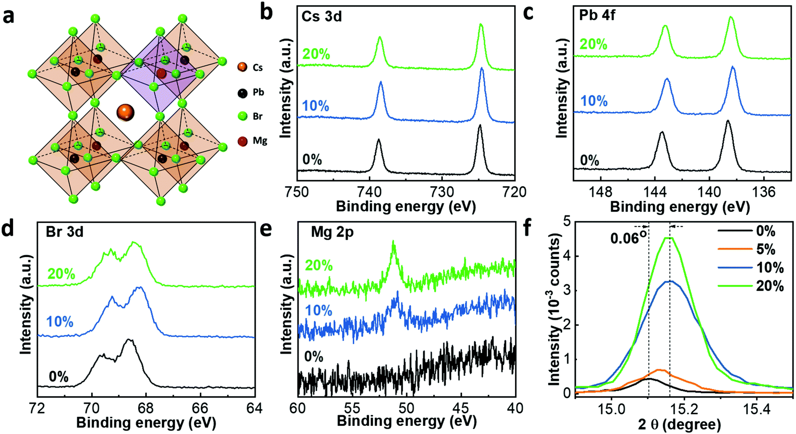 | ||
| Fig. 1 (a) Crystal structure of Mg-doped all-inorganic CsPb1−xMgxBr3 perovskite. XPS spectra of (b) Cs 3d, (c) Pb 4f, (d) Br 3d, (e) and Mg 2p regions and (f) XRD diffraction around 2θ = 15° of CsPb1−xMgxBr3 perovskite films with different MgBr2 concentrations. | ||
In order to further confirm the replacement of Pb2+ with Mg2+, θ–2θ X-ray diffraction (XRD) measurements were performed, since changes in the crystal lattice are expected if Mg2+ ions with a smaller radius replace Pb2+ (Fig. S1a, ESI†). Three typical diffraction peaks located at 15.1°, 21.4° and 30.6° can be observed, which correspond to the (100), (110) and (200) planes of a Pm![[3 with combining macron]](https://www.rsc.org/images/entities/char_0033_0304.gif) m cubic perovskite structure respectively.33 The peaks located at 27.60° and 29.32° are ascribed to CsPb2Br5 due to the corrosion of the perovskite film under ambient conditions (high humidity over 80%). A much stronger diffraction intensity from the (100) plane was observed in the perovskite films with Mg2+ incorporation, as shown in Fig. 1f. This peak became stronger with increasing ratio of MgBr2, indicating better crystallinity of the perovskite film. In addition, as we can see from the normalized XRD spectra in Fig. S1c (ESI†), the diffraction peak of the (110) plane almost disappeared while the diffraction peak of the (200) plane became stronger with increasing amount of MgBr2, which indicates the preferential orientation with Mg2+ substitution. Moreover, XRD peaks shifted toward a larger angle for Mg2+ incorporated films (Fig. 1f). The diffraction peak shifted from 15.10° (0%) to 15.16° (10%) suggesting the shrinkage of perovskite crystal lattice dimensions, which further proves that Pb2+ has been partially replaced with Mg2+. If instead Mg2+ ions were interstitially occupied between perovskite frameworks, a lattice expansion in the XRD pattern could be observed.34 Further theoretical calculations also demonstrated that the Mg–CsPbBr3 structure is stable with the Pb2+ site substituted with Mg2+ ions. The optimized structure is shown in Fig. S2a (ESI†), and the structure preserves the original symmetry without distortion. The partial density of states (PDOS) for the Mg–CsPbBr3 structure were calculated and are plotted in Fig. S2b (ESI†). After substituting the Pb2+ site with Mg2+, the electronic coupling interaction between Mg2+ and Br− does not generate any gap states around the Fermi level. Therefore, according to the experimental and theoretical results, it is safely concluded that Pb2+ ions are partially replaced by Mg2+ ions. Fig. S1b (ESI†) shows the full width at half maximum (FWHM) of the (100) peaks of perovskite films with different substitution concentrations. According to the Debye–Scherrer equation, D = Kλ/(β
m cubic perovskite structure respectively.33 The peaks located at 27.60° and 29.32° are ascribed to CsPb2Br5 due to the corrosion of the perovskite film under ambient conditions (high humidity over 80%). A much stronger diffraction intensity from the (100) plane was observed in the perovskite films with Mg2+ incorporation, as shown in Fig. 1f. This peak became stronger with increasing ratio of MgBr2, indicating better crystallinity of the perovskite film. In addition, as we can see from the normalized XRD spectra in Fig. S1c (ESI†), the diffraction peak of the (110) plane almost disappeared while the diffraction peak of the (200) plane became stronger with increasing amount of MgBr2, which indicates the preferential orientation with Mg2+ substitution. Moreover, XRD peaks shifted toward a larger angle for Mg2+ incorporated films (Fig. 1f). The diffraction peak shifted from 15.10° (0%) to 15.16° (10%) suggesting the shrinkage of perovskite crystal lattice dimensions, which further proves that Pb2+ has been partially replaced with Mg2+. If instead Mg2+ ions were interstitially occupied between perovskite frameworks, a lattice expansion in the XRD pattern could be observed.34 Further theoretical calculations also demonstrated that the Mg–CsPbBr3 structure is stable with the Pb2+ site substituted with Mg2+ ions. The optimized structure is shown in Fig. S2a (ESI†), and the structure preserves the original symmetry without distortion. The partial density of states (PDOS) for the Mg–CsPbBr3 structure were calculated and are plotted in Fig. S2b (ESI†). After substituting the Pb2+ site with Mg2+, the electronic coupling interaction between Mg2+ and Br− does not generate any gap states around the Fermi level. Therefore, according to the experimental and theoretical results, it is safely concluded that Pb2+ ions are partially replaced by Mg2+ ions. Fig. S1b (ESI†) shows the full width at half maximum (FWHM) of the (100) peaks of perovskite films with different substitution concentrations. According to the Debye–Scherrer equation, D = Kλ/(β![[thin space (1/6-em)]](https://www.rsc.org/images/entities/i_char_2009.gif) cosθ), where D is the average crystal size, K is the Scherrer constant, λ is the X-ray wavelength, β is the FWHM of the diffraction peak, and θ is the diffraction angle, the extracted average crystal sizes of perovskite films with different substitution concentrations are approximately 76 nm (0%), 53 nm (5%), 43 nm (10%) and 54 nm (20%), respectively, as summarized in Table S1 (ESI†). The results indicate the reduction of crystal size with incorporation of Mg2+, which is in line with the scanning electron microscopy (SEM) images, as shown in Fig. 2a. The average crystal size difference could be attributed to the different nucleation and growth rates of perovskite films.
cosθ), where D is the average crystal size, K is the Scherrer constant, λ is the X-ray wavelength, β is the FWHM of the diffraction peak, and θ is the diffraction angle, the extracted average crystal sizes of perovskite films with different substitution concentrations are approximately 76 nm (0%), 53 nm (5%), 43 nm (10%) and 54 nm (20%), respectively, as summarized in Table S1 (ESI†). The results indicate the reduction of crystal size with incorporation of Mg2+, which is in line with the scanning electron microscopy (SEM) images, as shown in Fig. 2a. The average crystal size difference could be attributed to the different nucleation and growth rates of perovskite films.
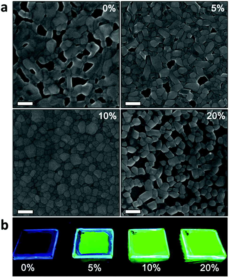 | ||
| Fig. 2 (a) SEM images for CsPb1−xMgxBr3 films with increasing Mg-content. All the scale bars are 200 nm. (b) Photographs of CsPb1−xMgxBr3 perovskite films under 365 nm illumination with different MgBr2 concentrations. The blue fluorescence is ascribed to the encapsulation with UV-curing adhesive. | ||
Replacement of Pb2+ with Mg2+ results in improved perovskite film morphology, as shown in Fig. 2a. The control sample without MgBr2 is composed of discrete large grains with numerous pin-holes, which would lead to a direct contact between the hole transport layer (HTL) and the electron transport layer (ETL). Upon incorporating 5% MgBr2, the film morphology was significantly improved with reduced grain size and much fewer pin-holes. The film morphology was further improved with the addition of 10% MgBr2, leading to a smooth film with full coverage of densely packed small grains. Nevertheless, further increasing the molar ratio of MgBr2 (20%) led to a rougher film morphology with increased grain size, which may be ascribed to a surpassed tolerance due to the excess Mg2+ in the precursor solution.32 Moreover, Fig. S3 (ESI†) presents the energy dispersive X-ray spectroscopy (EDX) mapping images of the perovskite film incorporated with 10% MgBr2, which confirms a homogeneous dispersion of Mg element in the whole perovskite film.
Ultraviolet visible (UV-Vis) absorption and PL spectroscopy studies were performed to investigate the influence of Mg2+ substitution on the optical properties of perovskite films. As shown in Fig. 3a and b, a clear blue-shift is observed in both UV-Vis absorption and PL spectra for the perovskite films incorporated with Mg2+. This blue-shift becomes more obvious with increasing molar ratio of Mg2+, in which the PL peak shifts from 527 to 522 nm as the molar ratio of MgBr2 increases from 0% to 20%. A quantum confinement effect is usually used to explain optical blue-shifts; however, as we discussed above, the calculated crystal sizes are much larger than the Bohr radius (approximately 7 nm for CsPbBr3),33 which can rule out the possibility of a quantum confinement effect for the blue-shift. Therefore, the optical shift is likely to be ascribed to a change in the crystal lattice upon Pb2+ replacement with Mg2+ cations because the conduction band and upper valence band are strongly related to Pb s and p orbitals.35 This is consistent with previous reports, where an increase in the bandgap occurs when lead is substituted with alkaline-earth metals.36
 | ||
| Fig. 3 (a) UV-Vis absorption spectra, (b) PL spectra, (c) comparison of the initial carrier recombination, (d) comparison of the kinetics obtained from long time PL and TA measurements, (e) time-resolved PL kinetics, and (f) PLQY (excited at 365 nm at approximately 2.3 mW cm−2) of CsPb1−xMgxBr3 perovskite films with different MgBr2 concentrations deposited directly on quartz. | ||
To investigate the effects of Mg2+ substitution on the radiative and non-radiative channels within the perovskite films, time-resolved transient absorption (TA) and PL decay were recorded. The TA response was integrated from 510 to 515 nm. Strikingly, we observe that the initial loss of charge carriers, which is usually observed in the first few picoseconds following photoexcitation, is significantly reduced by the inclusion of the Mg2+ ions, as shown in Fig. 3c. This recombination is normally attributed to a non-radiative loss pathway. The absorption changes with the addition of Mg2+, thus the absolute value of ΔT/T at the bleach peaks varies between 0.8% and 2.2%. This plot is normalised to highlight the differences between the bleach kinetics of each sample but this normalization does not significantly alter the trends that are presented.
In addition, the TA measurements confirm the increased carrier lifetime observed by time resolved PL decay. Fig. 3d plots the comparison of decay kinetics for TA (tracking the total excitation population) and PL (tracking the luminescent part). These results show that the inclusion of Mg2+ has significantly reduced non-radiative recombination, as the PL and TA lifetimes move closer together with the inclusion of Mg2+. The bimolecular nature of the luminescence is confirmed by the dependence of decay rate on carrier density (Fig. S4, ESI†). The results reveal that the recombination remains bi-molecular with addition of Mg2+, confirming that this crystal is non-excitonic in nature.
From the TA kinetics we find that the lifetime of the excited state population increases from 21 ns (Mg2+ = 0%) to 50 ns (Mg2+ = 10%) upon addition of Mg2+. As shown in Fig. 3e, the PL-lifetime for the perovskite films incorporated with Mg2+ also increased, indicating a reduction of non-radiative decay pathways. The cubic-exponential fitted PL lifetimes for perovskite films with different Mg2+ substitution concentrations are summarized in Table S2 (ESI†). The PL-lifetime increases from 0.79 ns (0% Mg2+) to 3.80 ns (5% Mg2+) and 11.10 ns (10% Mg2+). For the 20% Mg2+ sample, the PL-lifetime slightly decreases to 6.12 ns. We note that the PL lifetime increases by an order of magnitude, which is larger than the expected variation of a factor four from the observed doubling of TA lifetimes. This suggests that the incorporation of Mg2+ leads to further changes in the recombination order, although identification of the detailed mechanism is beyond the scope of this study.
To quantitatively analyse the trap density of perovskite films with different Mg2+ substitution concentrations, the dark current of hole-only devices with a structure of ITO/CsPb1−xMgxBr3/MoO3/Ag (Fig. S5, ESI†) was measured under different applied biases to calculate the trap density according to the following equation37,38
Halide vacancies have been reported to be the common defects in both inorganic and organic halide perovskites.39 Herein, we propose that the Mg-incorporated CsPbBr3 crystal may possess a relatively higher defect formation energy compared to pristine CsPbBr3. To verify our assumption, first-principles calculations for the cubic crystal structure of CsPbBr3 and CsPb0.875Mg0.125Br3 with Br vacancies were carried out. The optimized configurations are shown in Fig. S7 (ESI†). We used a 2 × 2 × 2 supercell including 7 Pb atoms and 1 Mg atom in CsPb0.875Mg0.125Br3. Due to the smaller radius of the Mg atom, the lattice parameters of the CsPb0.875Mg0.125Br3 crystal were reduced by 2.5%. The formation energy of a Br defect in both CsPbBr3 and CsPb0.875Mg0.125Br3 was calculated. The Br-defect formation energy in the CsPb0.875Mg0.125Br3 crystal is higher by approximately 0.1 eV than that in the CsPbBr3 crystal, indicating that it is slightly more difficult to form the Br-defect in the Mg-incorporated CsPbBr3 structure. Though the formation energy difference is small (this may be due to the limited size of the simulation supercell), the simulation results still give some hints on the lower defective density for the Mg-incorporated CsPbBr3 structure, which is consistent with our experimental observations.
Because of the reduced trap states, enhanced PL is clearly observed from photographs of CsPb1−xMgxBr3 films excited with a UV lamp (365 nm) (Fig. 2b), where the perovskite films were deposited on glass and encapsulated with UV-curing adhesive. As a result, the PLQY values of perovskite films incorporated with different ratios of MgBr2 show an enhancement, in agreement with the PL kinetics (Fig. 3f). The PLQY of pure CsPbBr3 was below the detection limit, while the PLQY value of films incorporated with MgBr2 was enhanced from 4.25% (5%) to 15.73% (10%). Additionally, light stability of perovskite films with different Mg2+ doping ratios was studied, as shown in Fig. S8 (ESI†). With continuous UV light exposure for 6 h, the PL intensity just slightly decreased, especially for the 10% sample, which indicates the good stability of our MgBr2-doped perovskite films against light.
To test the impact of the improved optoelectronic properties and compact film morphology upon Mg2+ substitution on device performance, PeLEDs with a structure of ITO/TFB/PVK/CsPb1−xMgxBr3/TPBi/LiF/Al were fabricated, as shown in Fig. 4a. The normalized electroluminescence (EL) curves of devices incorporated with different amounts of MgBr2 in Fig. 4b indicate a small blue-shift compared with the pristine one, in agreement with the PL spectra. The current density–voltage–luminance (J–V–L) curve in Fig. 4c reveals that the leakage current drastically decreased by two or three orders of magnitude for the devices with Mg2+ substitution, which may be contributed by the improved film morphology. The device incorporated with 10% MgBr2 achieves the lowest leakage current owing to its compact and pin-hole-free film morphology as presented in the SEM images. On the other hand, the luminance significantly increased by two orders of magnitude in contrast to the one without Mg2+ substitution, which can be attributed to the much lower trap density with the incorporation of MgBr2. The device incorporated with 10% MgBr2 achieved the highest luminance of 25450 cd m−2, in comparison to a luminance of 935 cd m−2 for films without Mg2+ doping. Fig. 4d shows a working PeLED device incorporated with 10% MgBr2 driven at 4 V, which exhibits uniform bright green EL emission. Fig. 4e depicts the EQE versus luminance curves, where the EQE increased with the amount of MgBr2, except for the 20% one. When the active layer is substituted with 10% MgBr2, the device achieved the best performance with an EQE of 3.60%. Although the 10% MgBr2 perovskite structure achieves a PLQY of 15.7%, the inferior EQE value should be ascribed to the low out-coupling efficiency of this LED structure. Due to the large refractive index of the perovskite layer, only approximately 20–25% of light can escape out of a continuous and flat emitting layer.40 The detailed performance parameters of devices with different Mg2+ substitution concentrations are summarized in Table S3 (ESI†). We attribute the reduced performance of the device with 20% Mg2+ to the poor film morphology. We further measured the operational lifetime to evaluate the device stability. The EL intensity was continuously measured under a constant applied voltage with an initial luminance of approximately 100 cd m−2 under ambient conditions. The operational lifetime is defined as the time when the luminance decays to half of its initial value. As shown in Fig. 4f, the operational lifetimes of devices incorporated with different amounts of MgBr2 are 7 min (0%), 60 min (5%), 138 min (10%) and 38 min (20%) respectively, implying that the devices fabricated with 10% MgBr2 in the precursor solution exhibit a 20-fold improvement in stability.
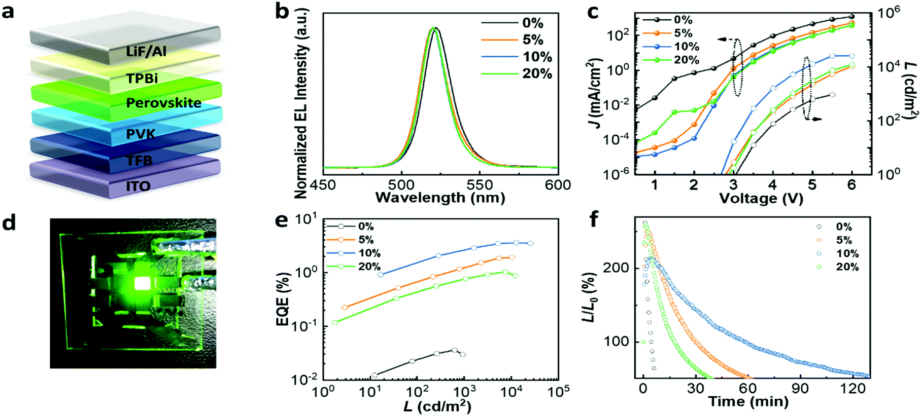 | ||
| Fig. 4 (a) Schematic of the PeLED devices. (b) EL spectra, (c) J–V–L curves, (d) photograph of a PeLED device fabricated with CsPb0.9Mg0.1Br3 precursor solution under 4 V bias. It shows the uniform emission range, (e) EQE–luminance dependence, (f) EL stability curves under a constant applied voltage of the devices based on the perovskite precursor solution incorporated with different amounts of MgBr2. All the devices show increased EL intensity in the first few minutes of measurement which then decayed with time. | ||
To gain detailed insights into the charge carrier injection and transfer processes in PeLED devices, we performed ultraviolet photoelectron spectroscopy (UPS) measurements on the Mg-doped films (Fig. 5a and b). The calculated work functions (WFs) are 4.74 eV (0%), 4.41 eV (10%) and 4.30 eV (20%) and the valence band maximum (VBM) values are 6.10 eV (0%), 5.74 eV (10%) and 5.87 eV (20%), respectively. According to the electronic bandgap extracted from the EL peak position, as shown in Fig. 4b, the corresponding conduction band minimum (CBM) values are calculated to be 3.72 eV (0%), 3.35 eV (10%) and 3.48 eV (20%), respectively. Fig. 5c presents the corresponding energy diagram calculated from the UPS spectra; the perovskite films incorporated with MgBr2 show a shallow VBM level, which is well in line with the theoretical research reporting that the VBM and CBM are strongly dependent on the Pb 6s and 6p orbital states.35,41 In our previous work, we demonstrated that the low hole injection rate in PeLEDs was one of the drawbacks that impeded device performance.42 For our device structure, the hole injection barrier is the main limitation for charge transport since the CBM of the perovskite layer is always under the lowest unoccupied molecular orbital (LUMO) level of TPBi as shown in Fig. S9 (ESI†). Because of the pulling up of the VBM, the hole injection barrier is decreased, and the hole injection rate is supposed to be improved, which is beneficial for fabricating high-performance PeLEDs. To be more specific, the VBM of 5.74 eV in the 10% perovskite film, since it is higher than the highest occupied molecular orbital (HOMO) level of PVK (5.8 eV), as shown in Fig. S9 (ESI†), results in the disappearance of the hole injection barrier, leading to balanced charge carrier injection and hence improved device performance. The falling back of the VBM of the perovskite film incorporated with 20% MgBr2 induces an injection barrier for holes, which is one reason for its worse performance.
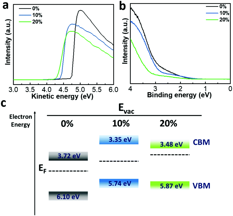 | ||
| Fig. 5 UPS spectra of perovskite films with different MgBr2 concentrations. (a) Work function, (b) offset between work function and ionisation energy. (c) Schematic illustration of the energy level change of the CBM, EF and VBM without and with incorporation of different MgBr2 concentrations. | ||
3. Experimental
Materials
PbBr2 (99.999%, metals basis) was purchased from Alfa. CsBr (99.999%, metals basis), LiF, Al (evaporation slug, 99.999%) and MgBr2 (99.999%, metals basis) were purchased from Sigma Aldrich. TFB, PVK and TPBi were purchased from Han Feng Chemical Co. Chlorobenzene (99.8% extra dry) and toluene (99.8% extra dry) were purchased from Acros. All the chemicals were directly used without any further purification.Preparation of perovskite precursor solutions
Precursor solutions were prepared according to the formula CsPb1−xMgxBr3, where x is the molar ratio of MgBr2, and the concentration of all kinds of precursor solutions is 0.2 mol L−1 in DMSO.Device fabrication
PeLEDs were fabricated on commercialized pre-patterned ITO glass substrates, which were ultrasonicated in acetone, ethanol and deionized water for 25 min each in sequence and then treated by ozone plasma for 15 min before depositing functional layers. Then, they were transferred to a N2-filled glovebox for spin coating of the TFB, PVK and perovskite layers. TFB (8 mg mL−1) in chlorobenzene was spin-coated with a speed of 1000 rpm for 40 s and baked at 120 °C for 20 min. PVK (4 mg mL−1) in toluene was spin coated on top of the TFB layer at 3000 rpm for 40 s and baked at 150 °C for 20 min. Then the perovskite precursor solutions filtered through polytetrafluoroethylene filter (0.45 μm) were spin coated via a two-step process at 1000 rpm for 5 s and 3000 rpm for 55 s respectively, followed by annealing at 90 °C for 20 min. Subsequently, the substrates were transferred into a vacuum thermal evaporator with pressure below 2 × 10⁻⁶ mbar; the TPBi (40 nm), LiF (1 nm) and Al cathode (100 nm) were deposited layer by layer, respectively. The active device area was 0.09 cm2.Characterization
The film morphology was characterized by SEM (Carl Zeiss (Supra 55)). Time resolved PL spectra were acquired on a fluorescence spectrophotometer (HORIB-FM-2015). PL spectra and PLQY (integrated with a sphere) were obtained using a fluorescence spectrophotometer (HORIBA FL3) excited by a 365 nm lamp with an excitation power density of 0.3 mW m−2. UV-Vis absorption spectra were acquired using a UV-Vis spectrometer (SPECORD S 600). XRD measurements were carried out with a Bruker D8 Advance X-ray diffractometer. XPS and UPS spectra were obtained using a SPECSTM photoelectron spectroscopy system with a monochromatized HeI (21.22 eV) excitation source. SEM-EDX was measured using a Gemini 500 and an Oxford Xmax 20. ICP-MS measurement was conducted with an Aurora M90. We directly deposited perovskite films on glass substrates. After annealing, the substrate was immersed in 0.5 wt% HNO3. The mass of the perovskite films was obtained from the weight difference of the glass substrates with and without the film. Later, the perovskite solutions were diluted and applied to conduct the ICP-MS measurement so that the real doping ratio of Mg2+ in the perovskite film can be obtained. The J–V–L characteristics and EL spectra were measured using a Keithley 2400 sourcemeter and a Photo Research spectrometer PR675. To obtain the ultrafast transient absorption data, a Ti:sapphire amplifier system (Spectra-Physics Solstice) operating at 1 kHz generated ∼100 fs pulses at 800 nm which were split into both pump and probe beam arms. The broad band probe beam (500–700 nm) was generated in a home-built noncollinear optical parametric amplifier, while the excitation was generated by second harmonic generation through a β-BBO crystal. The transmitted pulses were collected with an InGaAs dual-line array detector (Hamamatsu G11608-512) that was driven and read out using a custom-built board from Stresing Entwicklungsbüro. Long-time transient absorption (in the ns and μs regime) was similarly obtained, with the pump beam replaced by the third harmonic output (355 nm) from a Nd:YVO4 laser (AOT-YVO-25QSPX, Advanced Optical Technologies), with electronically controlled delay. The second set of time resolved photoluminescence measurements were obtained using an intensified charge-coupled device camera (Andor iStar DH740 CCI-010 system connected to a grating spectrometer Andor SR303i). Excitation at 400 nm was realized using a frequency-doubled Ti:sapphire laser (Spectra Physics Solstice) with a wavelength of 800 nm, repetition rate of 1 kHz and pulse length of ∼100 fs. Carrier density was obtained by measuring the film thickness (using a Bruker DektakXT Stylus Profilometer) and the absorption (using a UV-3600 Plus UV-Vis-NIR Spectrophotometer) for films of each composition in order to determine the absorption coefficient. The fluence was obtained in spectroscopy measurements, from spot size and power measurements, and converted to carrier densities using these absorption coefficients. The equation relating the carrier density and absorption coefficient is n0 = jα, where j is the pump fluence (photons cm−2) and α is the absorption coefficient (cm−1).43Computational method
The CsPbBr3 and CsPb0.875Mg0.125Br3 structures with Br-defects are optimized by the projector augmented wave (PAW) method within first-principles calculations as implemented in the Vienna ab initio simulation package (VASP).44 The Perdew–Burke–Ernzerhof (PBE) functional within the generalized-gradient approximation (GGA) was chosen to treat the exchange–correlation interaction of electrons.45 The Γ-centered K mesh of 3 × 3 × 3 is used with an energy cutoff of 450 eV for the plane-wave expansion of the electronic wave function. Geometric structures are fully relaxed until the force on each atom is less than 0.03 eV Å−1.4. Conclusions
In summary, we successfully demonstrate that Mg2+ cations can partially replace the Pb2+ ions in 3D perovskites for high-performance PeLEDs. The incorporation of MgBr2 can contribute to better crystallization as well as reducing the crystal size. In addition, better film morphology, enhanced PLQY, longer PL/TA-lifetime and decreased trap states were also achieved due to Mg2+ substitution, which is promising for fabricating high-performance PeLEDs. Moreover, the pulling up of both VBM and CBM levels of perovskite films with MgBr2 was beneficial for carrier injection in PeLEDs. PeLEDs based on the perovskite film with 10% MgBr2 achieved a bright luminance of 25450 cd m−2 and a current efficiency of 13.13 cd A−1 corresponding to an EQE of 3.60%. It is worth noting that a longer operation lifetime was also obtained as a result of Mg2+ substitution. Our work provides a feasible method to fabricate more efficient as well as low-toxicity PeLEDs, which paves the way for their further commercialization.
Conflicts of interest
There are no conflicts to declare.Acknowledgements
This work was supported by the National Key Research and Development Program of China (2016YFA0202402), the National Natural Science Foundation of China (61674108, 91833303), Jiangsu High Educational Natural Science Foundation (18KJA430012), the Priority Academic Program Development of Jiangsu Higher Education Institutions, the 111 program and Collaborative Innovation Center of Suzhou Nano Science and Technology (NANO-CIC). Y. T. Zou thanks the Postgraduate Research & Practice Innovation Program of Jiangsu Province (KYCX18_2504).References
- S. D. Stranks and H. J. Snaith, Nat. Nanotechnol., 2015, 10, 391 CrossRef CAS PubMed.
- W. S. Yang, B.-W. Park, E. H. Jung, N. J. Jeon, Y. C. Kim, D. U. Lee, S. S. Shin, J. Seo, E. K. Kim, J. H. Noh and S. I. Seok, Science, 2017, 356, 1376 CrossRef CAS PubMed.
- F. Deschler, M. Price, S. Pathak, L. E. Klintberg, D.-D. Jarausch, R. Higler, S. Hüttner, T. Leijtens, S. D. Stranks, H. J. Snaith, M. Atatüre, R. T. Phillips and R. H. Friend, J. Phys. Chem. Lett., 2014, 5, 1421–1426 CrossRef CAS PubMed.
- A. Kojima, K. Teshima, Y. Shirai and T. Miyasaka, J. Am. Chem. Soc., 2009, 131, 6050–6051 CrossRef CAS PubMed.
- Q. Lin, A. Armin, R. C. R. Nagiri, P. L. Burn and P. Meredith, Nat. Photonics, 2014, 9, 106 CrossRef.
- N. J. Jeon, H. Na, E. H. Jung, T.-Y. Yang, Y. G. Lee, G. Kim, H.-W. Shin, S. Il Seok, J. Lee and J. Seo, Nat. Energy, 2018, 3, 682–689 CrossRef CAS.
- G. Xing, N. Mathews, S. Sun, S. S. Lim, Y. M. Lam, M. Graetzel, S. Mhaisalkar and T. C. Sum, Science, 2013, 342, 344 CrossRef CAS PubMed.
- N. Pellet, P. Gao, G. Gregori, T.-Y. Yang, M. K. Nazeeruddin, J. Maier and M. Graetzel, Angew. Chem., 2014, 126, 3215–3221 CrossRef.
- W. Tress, J. P. Correa Baena, M. Saliba, A. Abate and M. Graetzel, Adv. Energy Mater., 2016, 6, 1600396 CrossRef.
- G. Li, Z. K. Tan, D. Di, M. L. Lai, L. Jiang, J. H. Lim, R. H. Friend and N. C. Greenham, Nano Lett., 2015, 15, 2640–2644 CrossRef CAS PubMed.
- Z.-K. Tan, R. S. Moghaddam, M. L. Lai, P. Docampo, R. Higler, F. Deschler, M. Price, A. Sadhanala, L. M. Pazos, D. Credgington, F. Hanusch, T. Bein, H. J. Snaith and R. H. Friend, Nat. Nanotechnol., 2014, 9, 687–692 CrossRef CAS PubMed.
- H. Cho, S.-H. Jeong, M.-H. Park, Y.-H. Kim, C. Wolf, C.-L. Lee, J. H. Heo, A. Sadhanala, N. Myoung, S. Yoo, S. H. Im, R. H. Friend and T.-W. Lee, Science, 2015, 350, 1222–1225 CrossRef CAS PubMed.
- K. Lin, J. Xing, L. N. Quan, F. P. G. a. de Arquer, X. Gong, J. Lu, L. Xie, W. Zhao, D. Zhang, C. Yan, W. Li, X. Liu, Y. Lu, J. Kirman, E. H. Sargent, Q. Xiong and Z. Wei, Nature, 2018, 562, 245–248 CrossRef CAS PubMed.
- Y. Cao, N. Wang, H. Tian, J. Guo, Y. Wei, H. Chen, Y. Miao, W. Zou, K. Pan, Y. He, H. Cao, Y. Ke, M. Xu, Y. Wang, M. Yang, K. Du, Z. Fu, D. Kong, D. Dai, Y. Jin, G. Li, H. Li, Q. Peng, J. Wang and W. Huang, Nature, 2018, 562, 249–253 CrossRef PubMed.
- B. Zhao, S. Bai, V. Kim, R. Lamboll, R. Shivanna, F. Auras, J. M. Richter, L. Yang, L. Dai, M. Alsari, X.-J. She, L. Liang, J. Zhang, S. Lilliu, P. Gao, H. J. Snaith, J. Wang, N. C. Greenham, R. H. Friend and D. Di, Nat. Photonics, 2018, 12, 783–789 CrossRef CAS.
- X. Dai, Z. Zhang, Y. Jin, Y. Niu, H. Cao, X. Liang, L. Chen, J. Wang and X. Peng, Nature, 2014, 515, 96–99 CrossRef CAS PubMed.
- P. J. Conaghan, S. M. Menke, A. S. Romanov, S. T. E. Jones, A. J. Pearson, E. W. Evans, M. Bochmann, N. C. Greenham and D. Credgington, Adv. Mater., 2018, 30, 1802285 CrossRef PubMed.
- F. Hao, C. C. Stoumpos, D. H. Cao, R. P. H. Chang and M. G. Kanatzidis, Nat. Photonics, 2014, 8, 489–494 CrossRef CAS.
- M. A. Green, A. Ho-Baillie and H. J. Snaith, Nat. Photonics, 2014, 8, 506 CrossRef CAS.
- M. H. Kumar, S. Dharani, W. L. Leong, P. P. Boix, R. R. Prabhakar, T. Baikie, C. Shi, H. Ding, R. Ramesh, M. Asta, M. Graetzel, S. G. Mhaisalkar and N. Mathews, Adv. Mater., 2014, 26, 7122–7127 CrossRef CAS PubMed.
- T. Yokoyama, D. H. Cao, C. C. Stoumpos, T. B. Song, Y. Sato, S. Aramaki and M. G. Kanatzidis, J. Phys. Chem. Lett., 2016, 7, 776–782 CrossRef CAS PubMed.
- M. T. Klug, A. Osherov, A. A. Haghighirad, S. D. Stranks, P. R. Brown, S. Bai, J. T. W. Wang, X. Dang, V. Bulović, H. J. Snaith and A. M. Belcher, Energy Environ. Sci., 2017, 10, 236–246 RSC.
- W. L. Hong, Y. C. Huang, C. Y. Chang, Z. C. Zhang, H. R. Tsai, N. Y. Chang and Y. C. Chao, Adv. Mater., 2016, 28, 8029–8036 CrossRef CAS PubMed.
- M. L. Lai, T. Y. S. Tay, A. Sadhanala, S. n. E. Dutton, G. Li, R. H. Friend and Z.-K. Tan, J. Phys. Chem. Lett., 2016, 7, 2653–2658 CrossRef CAS PubMed.
- H. C. Wang, W. Wang, A. C. Tang, H. Y. Tsai, Z. Bao, T. Ihara, N. Yarita, H. Tahara, Y. Kanemitsu, S. Chen and R. S. Liu, Angew. Chem., Int. Ed., 2017, 56, 13650–13654 CrossRef CAS PubMed.
- X. Sheng, Y. Liu, Y. Wang, Y. Li, X. Wang, X. Wang, Z. Dai, J. Bao and X. Xu, Adv. Mater., 2017, 29, 1700150 CrossRef PubMed.
- Z. Shi, Y. Li, Y. Zhang, Y. Chen, X. Li, D. Wu, T. Xu, C. Shan and G. Du, Nano Lett., 2017, 17, 313–321 CrossRef CAS PubMed.
- Z. Shi, S. Li, Y. Li, H. Ji, X. Li, D. Wu, T. Xu, Y. Chen, Y. Tian, Y. Zhang, C. Shan and G. Du, ACS Nano, 2018, 12, 1462–1472 CrossRef CAS PubMed.
- Z. Shi, Y. Li, S. Li, X. Li, D. Wu, T. Xu, Y. Tian, Y. Chen, Y. Zhang, B. Zhang, C. Shan and G. Du, Adv. Funct. Mater., 2018, 28, 1707031 CrossRef.
- C. F. J. Lau, X. Deng, J. Zheng, J. Kim, Z. Zhang, M. Zhang, J. Bing, B. Wilkinson, L. Hu, R. Patterson, S. Huang and A. Ho-Baillie, J. Mater. Chem. A, 2018, 6, 5580–5586 RSC.
- S. Zou, Y. Liu, J. Li, C. Liu, R. Feng, F. Jiang, Y. Li, J. Song, H. Zeng, M. Hong and X. Chen, J. Am. Chem. Soc., 2017, 139, 11443–11450 CrossRef CAS PubMed.
- X. Shai, J. Wang, P. Sun, W. Huang, P. Liao, F. Cheng, B. Zhu, S.-Y. Chang, E.-P. Yao, Y. Shen, L. Miao, Y. Yang and M. Wang, Nano Energy, 2018, 48, 117–127 CrossRef CAS.
- L. Protesescu, S. Yakunin, M. I. Bodnarchuk, F. Krieg, R. Caputo, C. H. Hendon, R. X. Yang, A. Walsh and M. V. Kovalenko, Nano Lett., 2015, 15, 3692–3696 CrossRef CAS PubMed.
- J. Cao, S. X. Tao, P. A. Bobbert, C. P. Wong and N. Zhao, Adv. Mater., 2018, 30, e1707350 CrossRef PubMed.
- W. Yang, Y. Tang, Q. Zhang, L. Wang, B. Song and C. Wong, Ceram. Int., 2017, 43, 13101–13112 CrossRef CAS.
- M. Pazoki, T. J. Jacobsson, A. Hagfeldt, G. Boschloo and T. Edvinsson, Phys. Rev. B, 2016, 93, 144105 CrossRef.
- M. A. Lampert, Phys. Rev., 1956, 103, 1648–1656 CrossRef CAS.
- A. A. Zhumekenov, M. I. Saidaminov, M. A. Haque, E. Alarousu, S. P. Sarmah, B. Murali, I. Dursun, X.-H. Miao, A. L. Abdelhady, T. Wu, O. F. Mohammed and O. M. Bakr, ACS Energy Lett., 2016, 1, 32–37 CrossRef CAS.
- D. Yang, W. Ming, H. Shi, L. Zhang and M.-H. Du, Chem. Mater., 2016, 28, 4349–4357 CrossRef CAS.
- X.-B. Shi, Y. Liu, Z. Yuan, X.-K. Liu, Y. Miao, J. Wang, S. Lenk, S. Reineke and F. Gao, Adv. Opt. Mater., 2018, 6, 1800667 CrossRef.
- J. Kang and L.-W. Wang, J. Phys. Chem. Lett., 2017, 8, 489–493 CrossRef CAS PubMed.
- Y. Zou, M. Ban, Y. Yang, S. Bai, C. Wu, Y. Han, T. Wu, Y. Tan, Q. Huang, X. Gao, T. Song, Q. Zhang and B. Sun, ACS Appl. Mater. Interfaces, 2018, 10, 24320–24326 CrossRef CAS PubMed.
- J. S. Manser and P. V. Kamat, Nat. Photonics, 2014, 8, 737 CrossRef CAS.
- K. Momma and F. Izumi, J. Appl. Crystallogr., 2011, 44, 1272–1276 CrossRef CAS.
- J. P. Perdew, K. Burke and M. Ernzerhof, Phys. Rev. Lett., 1996, 77, 3865–3868 CrossRef CAS PubMed.
Footnotes |
| † Electronic supplementary information (ESI) available. See DOI: 10.1039/c9nh00066f |
| ‡ These authors contributed equally to this work. |
| This journal is © The Royal Society of Chemistry 2019 |