
Doping engineering and functionalization of two-dimensional metal chalcogenides
Peng
Luo
,
Fuwei
Zhuge
*,
Qingfu
Zhang
,
Yuqian
Chen
,
Liang
Lv
,
Yu
Huang
,
Huiqiao
Li
and
Tianyou
Zhai
 *
*
State Key Laboratory of Material Processing and Die & Mould Technology, School of Material Science and Engineering, Huazhong University of Science and Technology, Wuhan, 430074, China. E-mail: zhugefw@hust.edu.cn; zhaity@hust.edu.cn
First published on 2nd August 2018
Abstract
Two-dimensional (2D) layered metal chalcogenides (MXs) have significant potential for use in flexible transistors, optoelectronics, sensing and memory devices beyond the state-of-the-art technology. To pursue ultimate performance, precisely controlled doping engineering of 2D MXs is desired for tailoring their physical and chemical properties in functional devices. In this review, we highlight the recent progress in the doping engineering of 2D MXs, covering that enabled by substitution, exterior charge transfer, intercalation and the electrostatic doping mechanism. A variety of novel doping engineering examples leading to Janus structures, defect curing effects, zero-valent intercalation and deliberately devised floating gate modulation will be discussed together with their intriguing application prospects. The choice of doping strategies and sources for functionalizing MXs will be provided to facilitate ongoing research in this field toward multifunctional applications.
 Peng Luo | Peng Luo received his BS degree from Northeastern University (NEU), China, in 2016. He is currently a PhD candidate at the School of Materials Science and Engineering, Huazhong University of Science and Technology (HUST). His research concentrates on the synthesis of 2D transition metal chalcogenides by CVD methods and their doping engineering for high performance electronic and optoelectronic applications. |
 Fuwei Zhuge | Fuwei Zhuge received his PhD degree from Shanghai Institute of Ceramics, Chinese Academic of Sciences in 2011. He then joined Osaka University and Kyushu University as a postdoctoral researcher. He is now an Associate Professor at the School of Materials Science and Engineering, Huazhong University of Science and Technology (HUST). His research interests have been focused on the controllable fabrication and application of various low-dimensional nanostructured materials in photodetection, energy storage and conversion. |
 Tianyou Zhai | Tianyou Zhai received his BS degree in Chemistry from Zhengzhou University in 2003 and then received his PhD degree in Physical Chemistry from the Institute of Chemistry, Chinese Academy of Sciences (ICCAS) under the supervision of Prof. Jiannian Yao in 2008. Afterwards, he joined in National Institute for Materials Science (NIMS) as a JSPS postdoctoral fellow of Prof. Yoshio Bando's group and then as an ICYS-MANA researcher within NIMS. Currently, he is a Chief Professor at the School of Materials Science and Engineering, Huazhong University of Science and Technology (HUST). His research interests include the controlled synthesis and exploration of the fundamental physical properties of inorganic functional nanomaterials, as well as their promising applications in energy science, electronics and optoelectronics. |
1. Introduction
2D MXs have been attracting increasing interest over the past few years due to their attractive carrier mobility,1,2 widely adjustable bandgaps,3 and their peculiar excitonic4,5 and light–matter interaction properties.6 As the counterparts of graphene, their rich physical and chemical properties have raised exotic prospects in optoelectronics,7–10 transistors,11–13 chemical14 and bio-sensors,15 memory,16 wearable devices,17 and recently in neuromorphic electronics.18 After years of efforts, the large-scale synthesis of many MXs with atomic-level thickness has become attainable based on both liquid exfoliation19 and chemical vapour deposition (CVD) methods.20–23 This has been mostly highlighted by the recent progress in synthesizing 47 kinds of MXs and some alloyed heterostructures using the melt-salt assisted CVD process.24 On this basis, the ability to precisely tailor their functional performances in applications is increasingly vital, which significantly relies on the doping engineering of these 2D MXs.25The prevailing 2D MXs compounds are generally comprised of cationic elements in the transition metal group (Mo, W, Ta, Nb, etc.), group IIIA (Ga, In) and IVA (Sn, Pb), and anionic elements of chalcogenides (O, S, Se, Te), which are bonded in the chemical formula MXn with n = 2, for the most part, e.g. for MoS2, WS2, etc., and n = 1, e.g. InSe, SnS, SnSe, etc.24,26,27 Because of the rich electron configurations in the d-orbitals of both the metal elements and chalcogenides (Se, Te),28 diverse electrical properties have been found in MXs compounds, ranging from semiconductors (MoS2, WS2)29 to insulators (HfS2)30 and even metals (NbS2).31 In particular, their characteristics, including doping polarity,32,33 optical luminescence34,35 and catalytic activity,36–38 have been demonstrated to be widely tuneable by a variety of doping engineering methods. Novel phase transition phenomena in terms of both crystal structure and electrical properties were also found in MoTe2 and TaS2 under high concentration charge injection.39–41 The rich properties of 2D MXs thus offered a wealth of opportunities for both fundamental studies and technological applications of their functional devices.
Based on the history of the contemporary Si and III–V semiconductors, the doping engineering of 2D materials appears to be the key to controlling their electronic,42 optical,43,44 magnetic,45,46 catalytic,36,37 and many other exotic properties including charge density wave,40 valleytronics,47etc. Fortunately, the ultrathin nature of 2D materials not only allows traditional substitutional doping strategies by implantation48 or diffusion processes,25,49,50 but also enables new methods that could address the demands; e.g. using surface charge transfer,51 intercalation52,53 and field effect modulation methods.54 The rich choices of doping strategy and sources are now rendering exciting opportunities in bringing new properties and functions to 2D MXs. A striking example is that the preferential substitution of single S layer in MoS2 to Se led to a new Janus-type 2D material (MoSSe) that has broken symmetry along the Z direction, thus leading to new applications in second harmonic generation (SHG),55 piezoelectricity,56 and improved catalytic performances in the hydrogen evolution reaction (HER).57
In this review, we summarize the recent progress in the doping engineering of 2D MXs and highlight their essential functions in various kinds of devices. The principle of each doping strategy, based on substitutional doping, charge transfer doping, intercalation doping and electrostatic doping, will be presented, followed by an in-depth discussion of their latest progress toward functional engineering and the remaining challenges for ongoing research efforts.
2. Strategies for doping 2D metal chalcogenides
The purpose of doping 2D materials is to achieve precise control of their electrical, optical and magnetic properties, and it is important to choose the appropriate doping method. Fig. 1 illustrates the primary strategies that are currently being used to achieve doping engineering in 2D MXs, including (i) substitutional doping, (ii) charge transfer doping, (iii) intercalation doping and (iv) electrostatic field effect doping. Compared to the conventional semiconductors with 3D crystal structures, which are usually doped by impurity atoms at substitutional or interstitial sites, the weak van der Waals (vdW) interactions between 2D layers lead to large interlayer distances that facilitate the intercalation of dopant atoms.52,53 When they are exfoliated or directly grown into ultrathin thicknesses, they can be also easily doped via surface charge transfer and external electrostatic field effects.54 Although in as-prepared 2D MXs, cation or anion vacancies are generally present due to slight stoichiometry differences, it is hard to regulate intentional doping. For example, the CVD-grown 2D MXs often appear in both triangular and hexagonal shapes due to the fluctuation of vapour sources and the local deficiency of anion or cation atoms.58–60 Deliberate post-treatments have been formulated to alleviate and eliminate the defects, e.g. by drafting thiol-containing molecules,61,62 ethylenediaminetetraacetic acid (EDTA)63 or coating poly(4-styrenesulfonate) (PSS) polymers,64 since they often lead to low carrier mobility and poor photoluminescence (PL) efficiency.42,65,66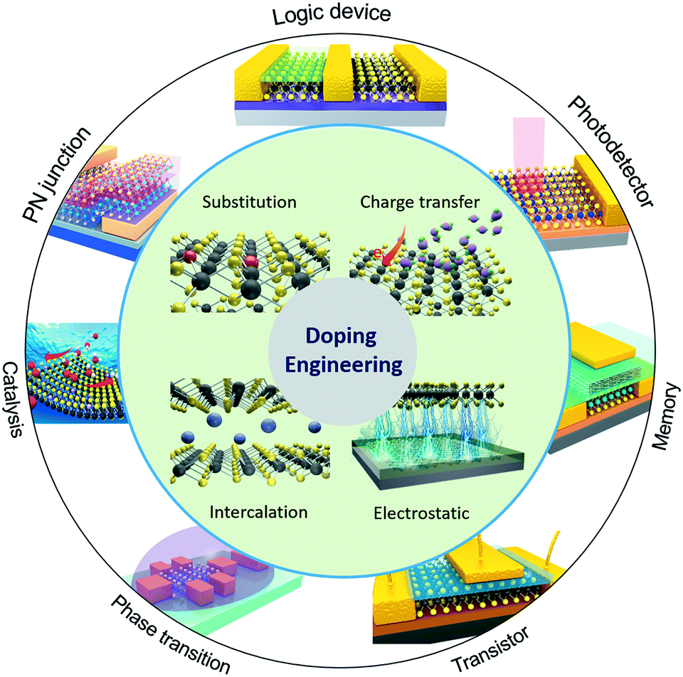 | ||
| Fig. 1 Doping strategies to 2D MXs and their potential function applications. | ||
To conduct the doping engineering in 2D MXs, one needs to choose the appropriate strategies according to the application purpose and then select the available doping sources and processing methods, e.g. using simple electrostatic doping for integrated electronic devices.54 It should be noted that the targeted application function, e.g. electrical modulation, is not exclusive to the doping strategies. For electrical purposes, one generally tunes the materials into either non-degenerate or degenerate n-type or p-type conductance with electrons and holes, respectively, as the majority carriers. In addition to electrostatic methods, this could be also achieved conventionally using substitutional doping at the anion or cation sites of the crystal lattice. The doping behavior is generally determined from their valence states, compared to the replaced elements in the lattice, with a subvalent replacement for p-type doping and a supervalent replacement for n-type doping, as will be discussed later. Another growing method is via charge transfer doping,51 in which the dopant source is attached to the surface of 2D MXs via either chemical bonds or physical interaction. According to their work function difference, electrons are injected into or withdrawn from MXs, thereby modulating their electrical conductance. Compared to substitutional doping, charge transfer doping does not create lattice disorders and is thus preferred to maintain high electrical mobility in ultrathin 2D MXs, as with field-effect modulation in electrostatic doping.54
The feasibility in scaling and patterning the doping process is another important factor, especially for integrated devices that require selective area doping, like detectors, logic inverters, memories, and transistors.44 Electrostatic doping has been generally adopted in such devices, which relies on the local patterning of gate dielectrics and electrodes by using lithography processes.43 However, keeping the field effects in devices draws continuous energy consumption in operation. Recently, substantial improvements have been made by using a floating gate and ferroelectric dielectrics in devices,67 which introduces retentivity to electrostatic doping. On the other hand, surface charge transfer doping of 2D MXs could be also feasibly patterned using the existing complementary metal oxide semiconductor (CMOS) technology,51 displaying bright potential in the assembly of functional devices.
There are many versatile possibilities of the various doping strategies and their functions. In the following sections, we generally classify the doping strategies into substitutional doping, charge transfer doping, intercalation doping and electrostatic doping. In each part, an in-depth survey will be provided regarding the latest progress in the doping engineering of 2D MXs. The advances in optimizing their performances in various functional devices will be also highlighted.
3. Substitutional doping
In MXs, both cationic and anionic elements can be substitutionally replaced by foreign atoms with comparable radii.68,69 Depending on the number of valence electrons in the dopant atom, the MXs can be doped into n-type70 or p-type conductance,32 and even with new optical emission.71,72 In the following, the theoretical aspects of substitutional doping will be firstly introduced by taking MoS2 as the example, and then the recent advances in doping metal-chalcogenides at cation and anion sites will be discussed.3.1 The theoretical aspects of substitutional doping
In the typical MXs crystal lattice, like the one displayed in Fig. 2a for MoS2, the metal atoms are generally sandwiched between the outer chalcogenide layers, which screens the incorporated metal atoms into the substitutional sites. Because of the length limitation of ionic bonds, non-metal dopants of MXs tend to occupy the anionic sites at the outer layers, while for metal dopants, the favourable position depends on the radii of the foreign dopant atoms. For light metals with smaller radii, such as Li and Na, the interlayer spaces (0.615 nm for MoS2) are usually large enough for intercalation, whereas for those heavy dopants with larger radii, i.e. the transition metals, substitutional doping is thermodynamically preferred.68,69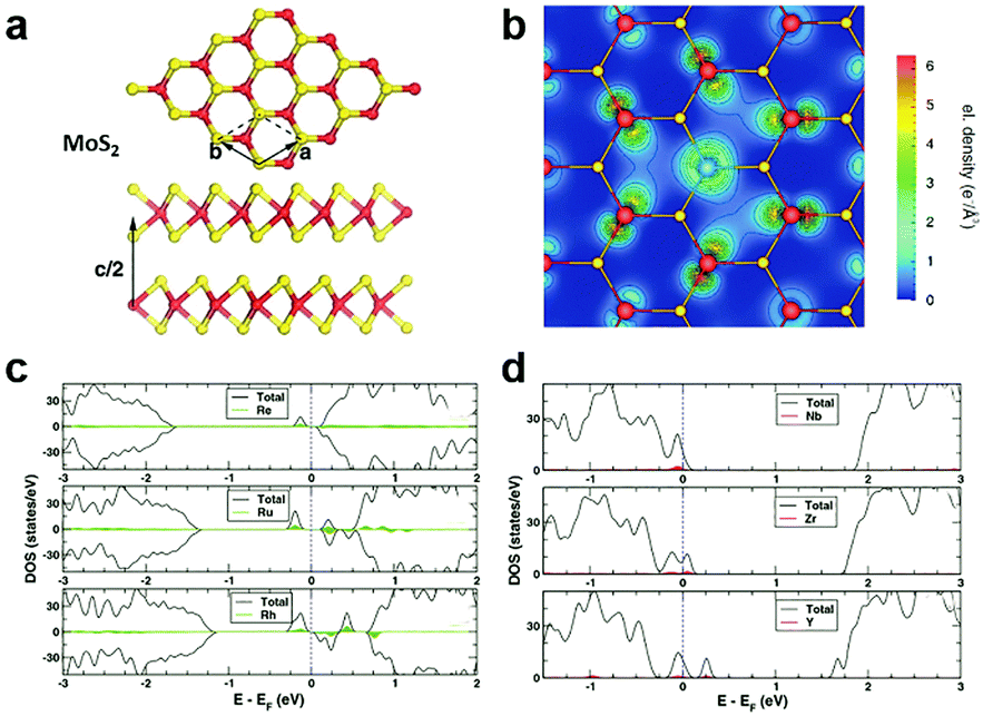 | ||
| Fig. 2 Substitutional doping of MoS2: (a) the crystal structure of MoS2 with Mo sandwiched between the S outer layers, (b) the electron density mapping of MoS2 with one Mo substituted by an Nb atom, reprinted with permission from ref. 79, Copyright 2008 American Physical Society. The electronic DOS of (c) Re, Ru, Rh and (d) Nb, Zr, Y substitutionally doped MoS2, reprinted with permission from ref. 69, Copyright 2013 American Physical Society. | ||
To determine the influence of substitutional doping, theoretical calculations based on first principles and density functional theory (DFT) are particularly instructive as the reference. The formation energy of substitutional doping and the resulting band structure, electronic density of states (DOS), and magnetic moments can be utilized to predict the thermal stability of the doping and the final electronic68,69,73 or magnetic properties.74,75 It has been shown that in MoS2, the formation energy of the S vacancy is considerably more negative than Mo vacancy,76,77 thus contributing to the usual n-type behaviour in the as-fabricated samples.78 Notably, the presence of native Schottky defects in MXs facilitates the formation of substitutional dopants at the vacancy position. As an example, the study on metal-sulfides showed that the doping of halogens (F, Cl, Br) and group V elements (N, P, As) at anion sites is more thermodynamically favourable in the presence of sulphur vacancies.69 At the metal sites, the formation of some dopants, such as Re in MoS2, also depends highly on the concentration of the metal vacancy. Doping of these elements into MXs compounds is, therefore, more favourably achieved in experiments using in situ methods during growth or post-treatments that create vacancy defects.
Considering the electrical behaviour, the impact of substitutional doping could be predicted from the calculated charge density distribution around dopant atoms and the electronic DOS. As displayed in Fig. 2b for substitutional Nb-doped MoS2,79 there is less electron density around the Nb atom than Mo, suggesting the acceptor behaviour of Nb in MoS2. This can be understood from the lower valence number of Nb (4d45s1) compared to Mo (4d55s1). The effect of valence electrons on whether the dopant atoms act as donors or acceptors was clearly revealed by the calculated electronic DOS (Fig. 2c and d).69 Those dopant elements (Re, Ru, Rh) with more valence electrons than Mo introduce electronic states below the conduction band minimum (CBM) and result in n-type doping, while the dopant (Y, Zr, Nb) with fewer valence electrons contributes, conversely, to p-type doping. Among the various substitutional elements, Re and Nb are hitherto the most extensively adopted doping elements in experiments for the n-type and p-type doping, respectively, in MoS2,32,50,80,81 while consistently, the latter was previously predicted as being thermodynamically practicable without the facilitation by vacancies.69,79
In addition to the modulation of electronic properties, the 2D MXs can also be doped by using magnetic elements such as Mn, Fe, Co.74,75 The ultrathin MXs can be engineered into dilute magnetic semiconductors that could find application in spintronic devices with feasible spin injection.82–84 However, the experimental realization of high-performance magnetic doping in MXs encounters the challenge of maintaining the electronic performances,45,85 because the incorporation of most magnetic dopant atoms still relies on vacancy defects in the lattice of MXs,83 which tend to limit the electronic performance.
In the past, the use of calculation power has greatly accelerated the screening of effective doping elements and designing the functionality of MXs. It should be however noted that the realistic material performance in experimental studies could be dramatically modulated by the co-existence of unguarded defect formation, which can, unfortunately, be required for the efficient incorporation of substitutional dopants. In Table 1, we summarize the electrical performance of several substitution-doped MXs at both the cation and anion sites, using the carrier concentration and mobility as the criteria.32,33,45,80,86–91 The effects of substitutional doping were seen as consistent with theoretical predictions, whereas their performances, e.g. the carrier mobility in devices, were greatly scattered for various reasons.
3.2 Cation substitutional doping
At the cation sites, many transition metal ions that have a similar radius to that of the host atoms can achieve effective substitutional doping of the MXs lattice, thus enriching the functionality.69 However, in the X–M–X structure, the encapsulating chalcogenide layers tend to act as blocking layers to the incorporation of foreign metal elements in post-treatment processes. It is, therefore, the usual case to achieve cation substitutional doping in situ during the fabrication of the MXs themselves, e.g. by tuning the source composition and the growth environments.32,46,49,50,80,81,86,92–97Using exfoliation methods, the ultrathin MXs with dopant modulation can be obtained from the doped bulk materials. Suh et al. first synthesized Nb-doped MoS2 bulk crystals using Mo, Nb, S and the source material.32 The nature of Nb substitutional doping at Mo sites (schematically illustrated in Fig. 3a) was confirmed by the study of the chemical bond environment by extended X-ray absorption fine structure (EXAFS) analysis. When exfoliated into few layers, the 0.5% Nb-doped MoS2 displayed strong p-type electrical conductance, as had been predicted.69 When assembled with non-doped MoS2, a vertical p–n junction with well-defined rectification characteristics was formed under positive gate modulation (Fig. 3b), which tuned the non-doped MoS2 into the n-type via the electrostatic effect. Notably, such degenerate Nb doping of >0.1% may cause structural transformation of MoS2 from the usual 2H (ABABAB) to 3R mode (ABCABC) stacking (Fig. 3c),49 which is asymmetric and inherently supports the SHG as a nonlinear optic material.98 It was also found to exhibit better catalytic activity in HER.99 Besides, after degenerate Nb doping, the PL properties of single-layer MoS2 were drastically shifted within 1.3 to 1.9 eV as displayed in Fig. 3d, due to the strong d-orbital coupling between the foreign dopants and the host Mo atoms.
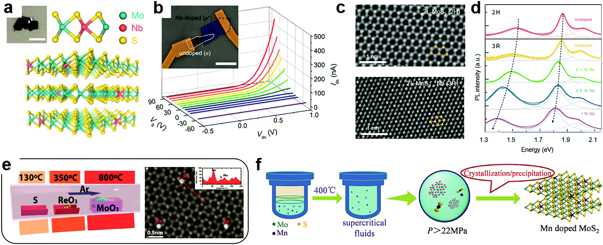 | ||
| Fig. 3 Substitutional doping at cation sites: (a) schematic illustration of substitutional Nb doping in MoS2 in partial replacement of Mo atoms, (b) the resulting rectification behaviour in a gate modulated junction formed between Nb-doped and undoped MoS2, reprinted with permission from ref. 32, Copyright 2014 American Chemical Society. (c) High resolution TEM image of bilayer MoS2 in the 2H and 3R phases induced by Nb doping and (d) their PL characteristics; reprinted with permission from ref. 49, Copyright 2018 Nature Publishing group. (e) A typical CVD configuration for in situ doping during growth using multiple source evaporation and the TEM image of the resulting Re doped MoS2, reprinted with permission from ref. 80, Copyright 2018, Wiley-VCH. (f) Illustration of hydrothermal procedures for achieving Mn doped MoS2 in supercritical conditions, reprinted with permission from ref. 108, Copyright 2017, Wiley-VCH. | ||
To fabricate large-scale and ultrathin MXs in the single crystalline or thin film form, the CVD methods are growing mature, considering the fact that some MXs (MoS2, WS2) could already be grown directly on dielectric substrate surfaces.21,22 Accordingly, there is increasing interest in achieving effective in situ dopant incorporation during the growth process. Metal halides, oxides, sulphides, tellurides, metal salts and pure metal elements could all be used as the candidates for source materials during CVD growth.100,101 The co-evaporation of multiple dopant sources and their rates could be controlled by using separately controlled temperature zones in CVD chambers or the temperature gradient, as the one indicated in Fig. 3e, thus offering the desired chalcogenide rich environment for MXs growth and dopant incorporation in cation sites.80
In 2016, Gao et al. successfully demonstrated the direct CVD growth of Nb and Re doped MoS2 and WS2 with monolayer thickness.50 The obtained Re concentration (0.3%) was much lower than that of Nb (6.7%) due to their large difference in the formation energy. To determine whether the dopant atoms are in the substitutional position, aberration-corrected Z-contrast scanning transmission electron microscopy (STEM) can be used to identify the Nb position in single layer MoS2. An indirect method has also been employed. For example, Lin et al. observed the stability of foreign dopant atoms under high dose electron beam irradiation.81 The surface adatoms of Au on MoS2 were found to migrate to the edges and vacancy sites when they gained sufficient energy from electron irradiation, while the substitutional Nb displayed excellent stability. The successful substitutional doping during CVD growth enabled the fine tuning of the electrical conductance of 2D MXs. The n-type dopant behaviour of Re doped samples greatly reduced the contact resistance in transistors.50 Recently, the Re dopant concentration in MoS2 was further increased to 1%, enabling degenerate n-type doping,80 and Nb doping was widely used for optimizing p-type transistors and other functional devices. For example, by artificially placing degenerate Nd-doped (0.5%) 2D WSe2 flakes at the contact, the obtained contact resistance to undoped WSe2 in the transistor was as low as 0.3 kΩ μm, yielding the high field-effect mobility of 200–300 cm2 V−1 s−1.102 In photodetectors, such degenerate 2D contact to WSe2 further helped to realize the ultrafast response time (8 μs) by effectively decreasing the RC time constant in the device.103
Notably, substitutional doping may induce structural disorder near the dopant.104 Increasing the concentration of substitutional doping in MXs by alloying may result in phase transformation rather than maintaining the host lattice structure. Kochat et al. found that MoSe2, which is thermally stable in the 2H phase, was transformed into the 1T′ phase after doping with Re to give the thermally stable structure of ReSe2.46 It is suspected that the 2H structure becomes unstable when lots of electrons are donated to the lattice under degenerate Re doping, similar to the case of the Li+ and Na+ intercalation-induced 1T phase.52 This structure transition was also observed in isoelectronic alloying systems, such as Mo1−xWxTe2,96 WxNb1−xSe2,105 and in WSe2(1−x)Te2x with substitutional doping at the anion sites.106 The metallic 1T phase transformed by doping engineering was utilized in devices such as transistors and detectors to improve the contacts for their metallic characteristics.105,106 Between the metallic phase contact and the semiconductor phase, it has been shown that a composition gradient could further suppress the Schottky contact barrier.107
In addition to vapour phase methods, cation substitution doping can be also achieved in solution methods. However, because of the formation energy issue, the incorporation of cation substitutional dopants other than Nb is still generally facilitated by creating vacancies in the host lattice. This fabrication can be achieved by choosing metal deficient or chalcogenide rich conditions. Recently, Tan et al. successfully doped magnetic Mn into MoS2 by using the supercritical hydrothermal method (Fig. 3f).108 Under high temperature and pressure, the concentration of Mn in MoS2 reached 3% while having the Mn2+ valence for room temperature ferromagnetism.
Though cation substitutional doping enriches the functionality of MXs, a critical challenge lies in the preferential patterning of the dopant for junction type electronic devices, since all the present methods ubiquitously rely on transfer methods that are unlikely to be scalable for integrated designs in the future. Developing substitutional doping methods that are temperature benign is however hindered by the high formation energy at cation sites, which deserves further attention.
3.3 Anion substitutional doping
Compared to the substitutional doping at cation sites, the anion substitutional doping can be more conveniently achieved in experiments. This is because in the structure of MXs, anion atoms are generally exposed to the outer surface, and the substitutional doping is likely to happen in the presence of anion vacancies.69 In the past, the anion substitution has been widely realized by both in situ growth and post-treatment methods,55,89,90,109–112 while the latter can be made compatible with existing patterning techniques. Owing to its feasibility in both controlling the electrical conductance by using various doping elements that are available in the gas phase, such as H,55,113 O,110,114 Cl,91,115 N,116,117 P,33 patterned substitutional anion doping was extensively adopted in electronic devices to reduce the contact resistance,88,115 and to build up selective area p–n junctions.33Similar to the cationic case, substitutional doping at anion sites also rely on the diffusion of dopants to the vacancy sites. Li et al. first introduced isoelectronic doping of MoS2 by Se in the CVD method, obtaining alloyed 2D few-monolayer MoS2xSe2(1−x) with lateral tuned composition.111 In MXs, the valence band position is generally contributed by the d-orbital of the metal and the valence electron of chalcogenides.31 The substitution of chalcogenides in the lattice often causes changes in the energy bandgap and thereby, related optical properties. It has been demonstrated that isoelectronic doping at anion sites can reach high concentration uniform alloying for tuneable PL bands displayed in Fig. 4a. If modulating the evaporation temperature during growth, gradient dopant incorporation can be tailored in 2D MXs, forming the graded lateral heterojunction (Fig. 4b).118 Abrupt MoSe2–WSe2 lateral heterojunctions were obtained alternatively by sequentially vaporizing Mo and W sources.119 By carefully balanced source evaporation, e.g. using molecular sieves,112 similar growth was extended to fabricate WS2xSe2(1−x),89 ReS2xSe2(1−x).112 Since sulphides and selenides often display different electrical conductance behaviour in terms of the majority carrier, such abrupt or graded lateral junctions have been made into p–n junctions,89 manifesting good rectification characteristics for low dark current and self-powered photodetection.119
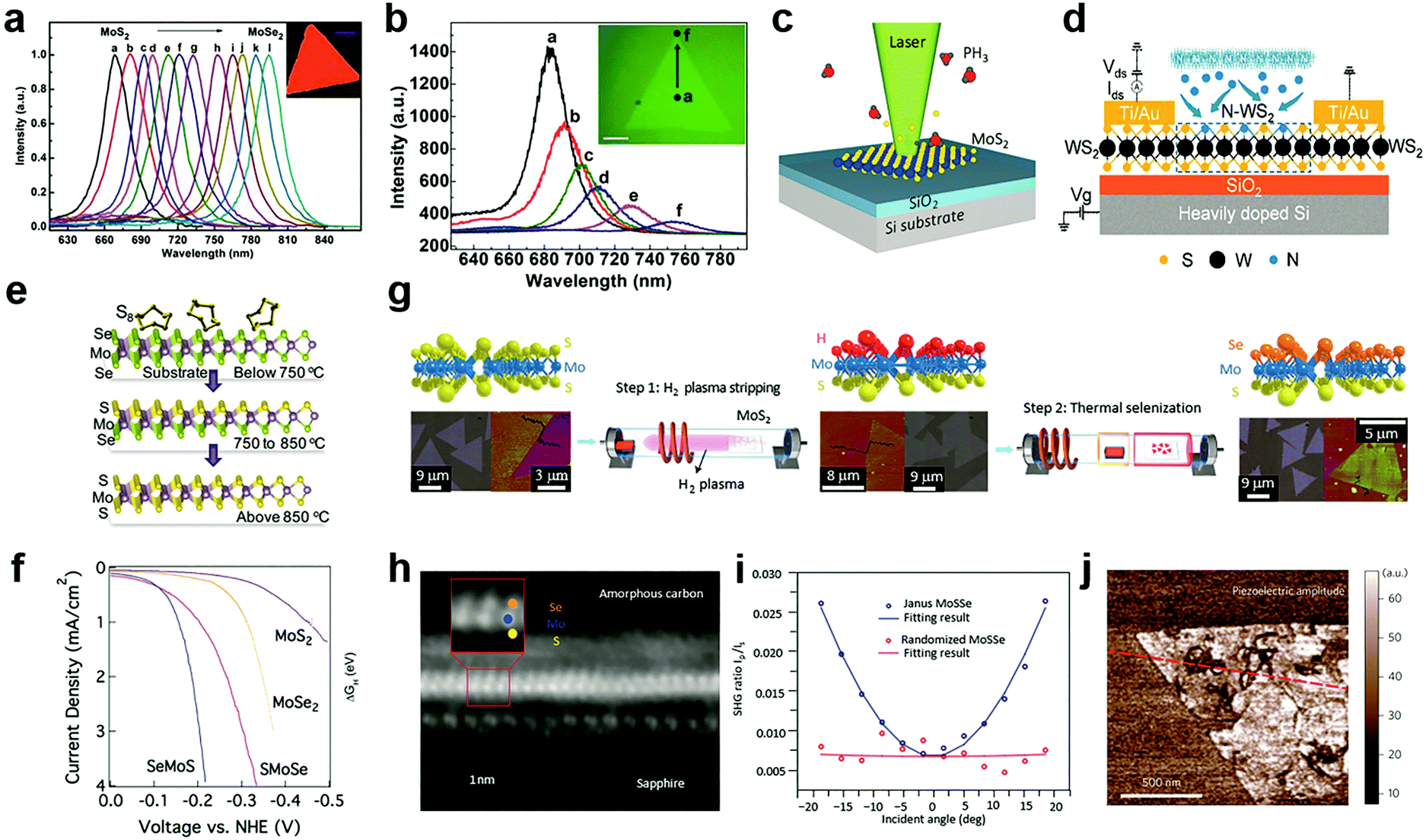 | ||
| Fig. 4 Substitutional doping at anion sites: (a) the PL of composition-tuned MoS2xSe2(1−x) with uniform distribution and (b) with composition gradient in a single flake, reprinted with permission from ref. 111 and 118, Copyright 2014, 2015 American Chemical Society. (c) Laser assisted selective area doping by PH3, reprinted with permission from ref. 109, Copyright 2016 American Chemical Society. (d) Schematic of N2 plasma doping of WS2, reprinted with permission from ref. 87, Copyright 2018 American Chemical Society. (e and f) 2D Janus structure of SMoSe from gentle sulfidation and the obtained HER performance, reprinted with permission from ref. 57, Copyright 2018 American Chemical Society. (g) H2 plasma-assisted fabrication of Janus type SeMoS, (h) the HRTEM image, (i) SHG, (j) piezoelectric properties, reprinted with permission from ref. 55, Copyright 2017 Nature Publishing group. | ||
Taking advantage of the ultrathin nature of MXs, anion doping can be also achieved by using two-step methods with gentle post treatments like thermal annealing. For example, by placing MoS2 thin flakes in a hot wall CVD chamber with Se powders, selenization was achieved at high temperature 750–800 °C.120,121 However, the high temperature involved in substitutional doping faces challenges when using lithography methods for patterned doping. By using gentle sputter processes that generate rich surface S vacancies on MoS2, Ma et al. were able to demonstrate 21% selenization using organic Se sources (diselenodiphenyl) at greatly reduced temperatures around 350 °C.122
In view of the challenge in patterned doping, Kim et al. developed a laser ablation assisted doping process.109 As displayed in Fig. 4c, the laser spot was focused to heat up the lattice (MoSe2) to generate anion vacancies and in the meantime cause the dissociation of PH3, which acted as the dopant source. The substitutional doping by the supervalent P occupying anion sites compensated for the intrinsic n-type doping in MoS2 while it enhanced the p-type conductance of WSe2. It is noteworthy that the doped 2D MXs displayed excellent ambient stability for over 30 days, having potential in selective area doping and contact engineering.109 An alternative solution is based on the plasma technique, which could be operated under mild temperature conditions and is compatible with the existing CMOS techniques. Various gas molecules including N2,117 O2,123 SF6,110 could be used to generate highly energetic ions using radio frequency methods. The energetic ions bombarding the surface of the 2D material are prone to create vacancies that facilitate dopant incorporation, while in some cases, they can be directly implanted into the lattice of MXs.
In 2016, Nipane et al. successfully doped MoS2 with both non-degenerate and degenerate p-type conductance by using inductively coupled PH3:H2 plasma treatment.33 The inductive coupling enabled feasible DC bias control to the kinetic energy of ions bombarding the surface of MoS2 flakes. The hole mobility in P-doped MoS2 after correcting contact resistance reached 8.4 and 137 cm2 V−1 s−1, respectively, for degenerate and non-degenerate doping. When combined with lithography patterning, the plasma treatment method enabled the fabrication of a p–n junction that had an optimized rectification ratio exceeding 2 × 104.33 However, for ultrathin 2D MXs down to the monolayer, the plasma method may cause significant crystal disorder due to the accompanying etching effects from the energetic ions.110 Recently, Tang et al. improved the apparatus by introducing a perpendicular electric field to restrain energetic ions, leaving only neutral atoms reaching the sample surface (Fig. 4d).87 The method enabled the effective p-type doping of WS2, down to the few-layer to monolayer thickness level, yielding a moderate hole mobility of 0.53 cm2 V−1 s−1 without correcting the contact resistance. On the other hand, Chen et al. utilized the artificial surface states of MoS2 created from highly energetic CF4 and O2 plasma treatments in fabricating multi-bit memory devices, which displayed ambipolar charge trapping lasting for days.110
The increasingly established surface modification methods on 2D MXs further enabled the design and fabrication of novel Janus structures with the broken symmetry of the chalcogenides anions.55,57Fig. 4e illustrates the fabrication of Janus type MoSSe.57 Unlike conventional doping that generates random dopant distribution, the S and Se atoms in the Janus structure are located regularly in opposite positions in the lattice. Since Se at the bottom layer requires higher energy to substitute for gaseous sulfur molecules compared to the upper layer, the replacement of only the surface atoms is possible under suitable temperature and pressure conditions. By using carefully controlled sulfurization and selenization after CVD growth, Zhang et al. successfully demonstrated the fabrication of SMoSe and SeMoS Janus structures.57 The exciton energy of SMoSe lies between that of MoSe2 and MoS2, which is similar to the case of MXs alloys. Notably, the SeMoS Janus structure with surface Se replacement displayed significantly improved hydrogen evolving reaction (HER) performance compared to either MoSe2 or MoS2, as indicated in Fig. 4f.57
Due to the broken symmetry, the Janus type MXs exhibited inherently dipolar characteristics and other distinct properties compared to the randomly formed alloy, including piezoelectric and SHG.55,56 Lu et al. fabricated the SeMoS Janus structure by first stripping off the surface S atoms from MoS2 using remote H2 plasma treatment, followed by a thermal selenization as indicated in Fig. 4g.55 Precisely controlled plasma power was used to preserve the underlying Mo–S structure. The vertical asymmetric Se–Mo–S (Fig. 4h) was demonstrated to be active for optical dipole transition, leading to the out of plane SHG. In the experiment, such out of plane SHG activity could be identified from an angular dependent measurement, as displayed in Fig. 4i. The SHG intensity was scaled with the projected vertical electric field of incident optical excitation.55 The Janus structure clearly displayed the piezoelectric response in experiments,55 which in principle could be engineered by increasing the dipole contrast between the upper and lower chemical bonds.56,124 The precisely controlled substitutional doping at anion sites may, therefore, have the potential for creating new materials with novel functional properties.
4. Charge transfer doping
Charge transfer doping has attracted much attention in modulating the electronic behaviour of semiconductors.51 In contrast to substitutional doping with foreign dopant atoms incorporated into the lattice, the charge transfer doping takes advantage of the charge transfer interaction between the host material and any adjacent mediums, including surface adatoms,125 ions,126 molecules,127,128 particles129–131 and supporting substrates.132–135 Since the dopants lie out of the transport pathways of electrical carriers, such modulated doping avoids lattice distortion and enables high mobility transport in low dimensional materials.51 Significant research efforts have therefore been devoted to exploring ideal dopants that offer efficient charge transfer doping and superior functional performances.4.1 Principle of charge transfer doping
In charge transfer doping, the dopants are placed in contact with the host materials, based on either physical or chemical interaction. The Fermi level difference between the dopant and the host materials determines the charge transfer direction, and whether the adsorbed dopant acts as an acceptor or a donor. As illustrated in Fig. 5a, when the dopant exhibits a lower Fermi level (EF) than the host semiconductor, electrons are withdrawn from the semiconductor to the dopants, thus causing p-type doping. Conversely, n-type doping is obtained when the dopants have higher EF than the semiconductor. For gas molecules, a similar analysis is made by considering the electronegativity, with the oxidizing molecules like O2136 and NO2128 as the p-type dopants, and reducing molecules as the n-type dopants.137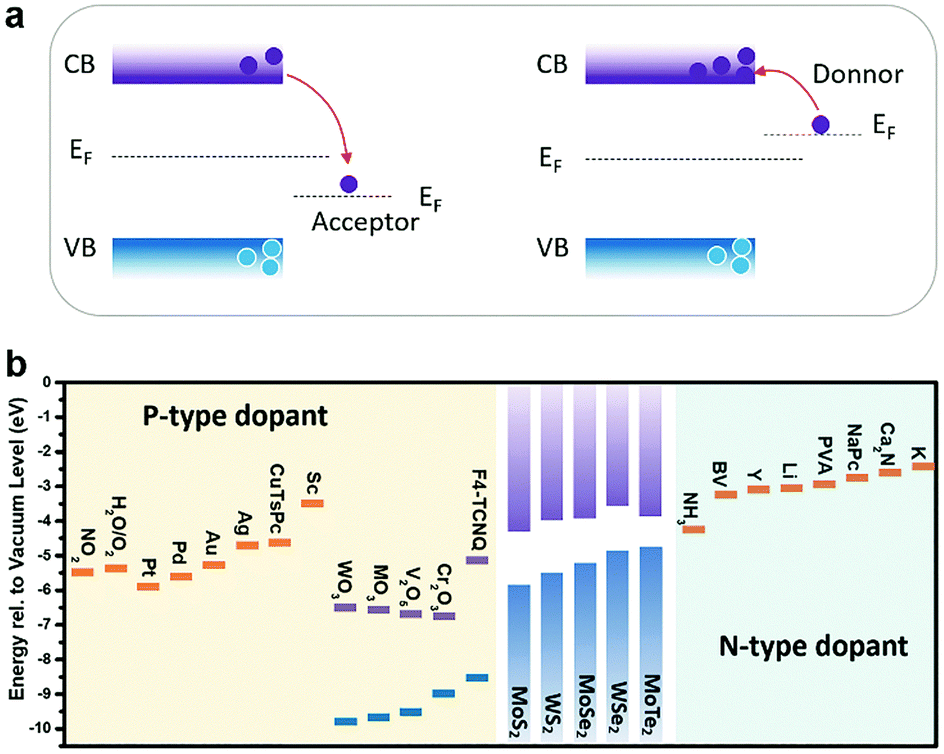 | ||
| Fig. 5 (a) Acceptor or donor behaviour of charge transfer doping of the semiconductor according to the Fermi level difference. (b) The summary of n-type and p-type dopants of typical MXs. | ||
Theoretical methods based on first principles and density functional theory can instead be used to predict the surface charge transfer to semiconductors and the resulting surface electronic states. The formation energy of surface adsorbents can verify the spontaneity of the adsorption process and predict the most thermally stable surface arrangement; the resulting electronic DOS then depicts the final electrical properties. The charge transfer direction between the host and surface adsorbents is directly visualized by the charge density distribution and their difference before and after the adsorption.138 Such theoretical methods are particularly viable for complicated molecules.139 However, for semiconductor organic molecules or others, the situation is much more complicated since the work function of the adsorbent and the resulting charge transfer behaviour are also influenced by the native doping and interface conditions.
For 2D materials, the ultrathin thickness and the exposed basal plane make their electrical properties especially sensitive through such charge transfer doping.51 The representative charge transfer dopants of several typical MXs, namely MoS2,126,131,134,138,140–142 WSe2,128,142–148 MoTe2,149,150 and InSe,151,152 are summarized in Table 2. In the following, we discuss their realization and performances using the classification of dopant sources as gaseous molecules, metals and metal compounds, organic small and super-molecules.
| MX2 | Dopant | Type | Concentration [cm−2] | Mobility [cm2 V−1 s−1] | Ref. |
|---|---|---|---|---|---|
| MoS2 | O2, H2O | p | — | — | 138 |
| AuCl3 | p | 1.5 × 10¹² | 68–132 | 131 | |
| FTOS | p | 3.4 × 10¹² | 0.087 | 134 | |
| ATO | n | 7.4 × 10¹² | 8 | 140 | |
| PVA | n | 8 × 10¹² | 36.6 | 141 | |
| BV | n | 1.2 × 10¹³ | 24.7 | 126 | |
| APTES | n | 1.0 × 10¹¹ | 142.2 | 142 | |
| WSe2 | NO2 | p | 2.2 × 10¹² | 250 | 128 |
| OTS | p | 1.4 × 10¹¹ | 168.8 | 142 | |
| MoO3 | p | 2 × 10¹³ | — | 147 | |
| WOx | p | 2.6 × 10¹² | 57 | 146 | |
| Au | p | — | 100 | 145 | |
| XeF2 | p | 5.18 × 10¹² | 0.35 | 143 | |
| K | n | 2.5 × 10¹² | 110 | 144 | |
| Cs2CO3 | n | ∼9× 10¹¹ | 27 | 148 | |
| MoTe2 | O2 | p | 5 × 10¹² | 80 | 150 |
| BV | n | 5.2 × 10¹² | 41 | 150 | |
| Ca2N | n | 1.6 × 10¹⁴ | — | 149 | |
| InSe | O2, H2O | p | — | 79.5 | 151 |
| Ti4+ | p | 5.25 × 10¹² | 4.1 × 10⁻³ | 152 | |
4.2 Gaseous molecules
In the atmosphere, foreign molecules are universally adsorbed on the surfaces of 2D MXs, which in turn modulate their optical and electronic behaviours.127,138,153 This feature is highly relevant to the gas sensing application that employs semiconductor materials as the sensing channel;14 it has recently been intentionally utilized to tune the performance of 2D materials.128,154Direct exposure of 2D materials to a target atmosphere is the simplest gas-phase doping method. The adsorption is mostly physical via weak vdW interactions, making it possible to desorb under vacuum conditions.138,153 The exposure effect to gas molecules is strengthened in samples after a so-called forming process by thermal annealing in a vacuum,138 which acts to clean unnecessary surface contaminants and creates chalcogenide vacancies that promote molecules adsorption. Tongay et al. have investigated the PL properties of n-type MoS2, MoSe2 and p-type WSe2 by exposing them to various gas atmospheres such as O2, H2O, ambient and inert gases.138 They found that the PL intensity in n-type MoS2 and MoSe2 can be dramatically enhanced by exposure to O2 and H2O, as indicated in Fig. 6a, due to the depletion of electrons and the related suppression of non-radiative Auger recombination (Fig. 6b). For p-type WSe2 the situation was reversed to deteriorate the PL efficiency. Since the amount of surface adsorption depends intimately on the concentration or pressure of the target gas molecules, the PL emission spectra and peak positions are strongly related to exposure conditions.138 Notably, the adsorption of gas molecules may preferentially adsorb on the edge, grain boundary or defect positions.153 Moving a step forward, a reinforced modulation of PL emission of MoS2 was demonstrated by chemically bonded O2 in mild plasma treatment.153
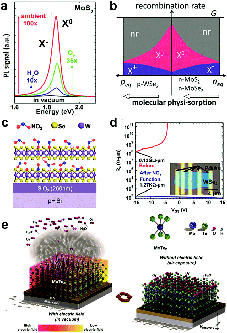 | ||
| Fig. 6 Gas molecules bound to 2D MXs: (a) the modulation of PL properties of MoS2 by exposure to various gas atmospheres; (b) the change in exciton and non-radiation recombination in p-type WSe2 and n-type MoS2, MoSe2, reprinted with permission from ref. 138, Copyright 2013 American Chemical Society. (c) Preferential NO2 binding to WSe2 at vacancy sites, forming WSe2−x−yOxNy species on the surface, and greatly reduced the contact resistance in transistors (d), reprinted with permission from ref. 155, Copyright 2014 American Chemical Society. (e) The engineering of gas molecules adsorption by electrothermal (left) and gate (right) modulation, reprinted with permission from ref. 127, Copyright 2018 Wiley-CH. | ||
On the surface of 2D MXs, the gas adsorption can be selective in a particular temperature range based on the different adsorption energy. Ou et al. investigated the gas sensor performance of SnS2 at <160 °C, and discovered the preferential response to NO2 over H2, CH4, CO2, H2S and NH3, as it was prone to bind strongly to surface vacancy sites.154 Due to the formation energy difference and strong charge transfer interactions, slight amounts of NO2, down to parts per million (ppm), could influence the electrical conductance of SnS2. Such simple surface adsorption could be transformed into covalently bonded chemical adsorption at elevated temperatures. Zhao et al. achieved p-type degenerate doping (>1019 cm−3) to WSe2 by NO2 surface treatment at 150 °C,155 which resulted in WSe2−x−yOxNy species on the surface, particularly at the Se vacancy sites, as illustrated in Fig. 6c. When combined with the pattern method, such gas phase treatment rendered remarkable improvement of contact resistance in Pd contacted field-effect transistors, from 0.13 GΩ μm to 1.27 kΩ μm (Fig. 6d). Such optimized contact by NO2 treatment resulted in an ideal sub-threshold swing (SS) of ∼60 mV dec−1 in the single layer WSe2 transistor.128
Beyond the lithography patterning, the gas phase adsorption can be controlled by using electrostatic fields from gate bias or electrothermal effects for advanced manipulation in devices. For example, Feng et al. found that under gate bias stress, O2 and H2O were attracted to the surface of InSe at Vg > 0, but were repelled when Vg < 0.151 The process was controlled not only by the polarity of the applied gate bias but was also related to the bias voltage and duration. By combining the gate effect and electrothermal effect, which desorbed surface adsorbents by Joule heating the 2D MoTe2 channel (Fig. 6e),127 Chang et al. recently demonstrated a facile construction of p/n-type doping in MoTe2, and also inverters, NOR and NAND logic devices. These results revealed the potential for adapting surface gas molecules adsorption induced doping in electronic devices.
4.3 Metals and metal compounds
By decorating metal144,156,157 or metal compounds, typically their ion complexes152 and oxides147,158,159 at the surface, 2D MXs can be intentionally doped. The decoration can be routinely made on 2D MXs by using evaporation and solution cast methods that are compatible with existing patterning techniques. As the essential criteria, it has been demonstrated that the work function of dopant sources (Fig. 5b) can predict well the resulting electrical doping behaviour, providing the guidelines for choosing dopants.Banerjee et al. comprehensively investigated the electrical doping of MoS2 and WSe2 with various noble metals nanoparticles (NPs: Au, Ag, Pd, Pt) and low work function metals (Sc, Y), prepared by electronic beam deposition methods.157 All the noble metals had larger work functions, >4.6 eV, and acted to deplete the original electron doping in MXs. In comparison, the Sc NPs (Φ = 3.5 eV) displayed only slight depletion effect, while Y NPs (Φ = 3.0 eV) with the lowest work function showed electron doping behaviour. Such a trend validates that the aforementioned higher work function dopants are prone to acting as p-type dopants by compensating the original electron concentration in n-type MXs. In particular, the MoS2 FET functionalized with Pd NPs displayed prospects in hydrogen sensing under such a charge transfer principle, based on the changeable work function of Pd NPs upon hydrogen adsorption.157
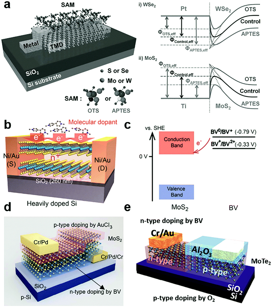
Since potassium has a low ionization energy and work function (2.3 eV), it was previously demonstrated to be very efficient for n-type doping in carbon nanotubes, graphene and recently in 2D MXs.51 By using a Joule heated K dispenser, Fang et al. investigated K doped MoS2 and WSe2. The amount of dopant was carefully controlled by the exposure time to K vapour and electrical characteristics of the device were observed in situ.144 The resulting electron concentration in MoS2 and WSe2 reached 1 × 1013 cm−2 and 2.5 × 1012 cm−2, respectively. Combined with a top-gate underlap structure (Fig. 7a), a selective area doped n+/i/n+ structure was demonstrated with remarkably suppressed electrical contact resistance in transistors, leading to improvement of the ON current by 4–5 orders (Fig. 7b). The extracted electron mobility in degenerately doped WSe2 exceeded 100 cm2 V−1 s−1. Later, a CMOS inverter was demonstrated in a single flake of WSe2 by combined contact electrode engineering (Pt for hole transport, Au for electrons) and K vapour doping.160 Other low work function dopants, such as amorphous TiO2 (ATO),140 Cs2CO3,148,161 and 2D electrides like Ca2N,149 have also been explored for n-type charge transfer doping of 2D MXs. When the single crystalline [Ca2N]+·e− electride was brought in close contact with MoTe2, ultrahigh degenerate (1.6 × 1014 cm−2) and long-range electron doping, penetrating 100 nm thickness, were recently demonstrated, leading even to a partial lattice symmetry change from 2H to 1T′. However, in spite of the strong electron doping effect, the poor air stability of K, Ca2N and similar low work function dopants in ambient conditions remains to be solved for integrated device fabrication.
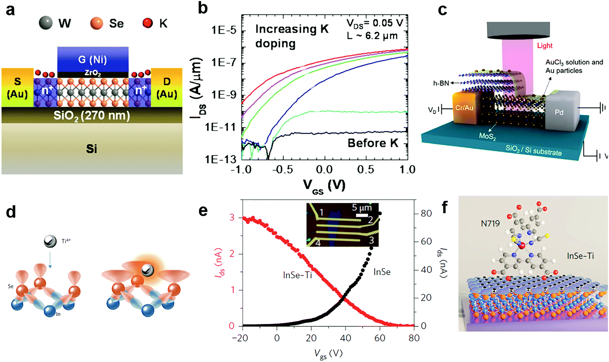 | ||
| Fig. 7 Charge transfer doping of MXs by metal and metal compounds: (a) K doping of WSe2 in a top gate transistor and (b) the resulting transfer curve, reprinted with permission from ref. 144, Copyright 2013 American Chemical Society. (c) Lateral PN junction enabled by AuCl3 doping of MoS2, reprinted with permission from ref. 129, Copyright 2014 American Chemical Society. (d) Schematic of Ti4+ Lewis acid bonding to the surface of InSe, (e) the transfer curve before and after doping, and (f) the schematic of a Lewis acid bridged connection to N719 dye molecules, reprinted with permission from ref. 152, Copyright 2017 Nature Publishing group. | ||
Due to the large positive reduction potential (1.4 V), AuCl3 is one of the most commonly used p-type dopants for 2D MXs.129–131,162 Though it was initially used to explore graphene,163 it has been widely adopted for tuning the doping polarity of n-type MXs. Liu et al. demonstrated the p-type doping of 2D MoS2 by spin-coating AuCl3 solution on it.131 The AuCl3 was later transformed into Au particles by accepting electrons from adjacent MXs. When other reductants such as NH2OH were included in the solution, the doping behaviour disappeared,156 demonstrating the critical role of surface reactions in the resulting doping behaviour. By using a partially pre-stacked h-BN as the mask (Fig. 7c), the group was able to fabricate a lateral MoS2 p–n junction with an ideal factor close to 1.129 Later, they further introduced a graphene buffer layer to the contact as the hole injection layer, then greatly lowered the contact resistance to 2.3 kΩ μm in the p-type transistor; the obtained hole mobility in MoS2 reached 72 cm2 V−1 s−1 at room temperature. From there on, a CMOS inverter was successfully fabricated based on the pristine n-type MoS2 and the degenerately p-doped MoS2.131 Recently, a vertical homogeneous MoS2 p–n junction was also reported based on diluted AuCl3 coating. The device upon illumination displayed ultrasensitive response to sub fW incident light power, reaching not only a high responsivity of 7 × 10⁴ A W−1 and superior detectivity of 3.5 × 10¹⁴ Jones, but also the fast response time on the scale of tens of ms.130 The intriguing performance demonstrated the potential for controllable surface chemical doping in the versatile engineering of device performances.
Due to the inert surface chemistry of 2D materials, chemically bonded charge transfer to MXs often relies on surface defects that inevitably degrade the material performances. Recently, a new strategy exploring Lewis acid (Ti4+, B3+, Al3+ and Sn4+) coupling to the lone pair electrons of the surface chalcogenide atom (Fig. 7d) was developed by Lei et al.152 Although the process is facile, achieved by solution treatment processes, the Lewis acid dopants were perfectly incorporated into the surface lattice of InSe by forming coordination complexes, as evidenced by an atom-resolved high angle annular dark field (HAADF) study. In the Mulliken population analysis, the surface bonded Ti4+ Lewis acid was found to withdraw 1.037 electrons from InSe, causing the p-type doping behaviour displayed in Fig. 7e. Importantly, such Lewis acid modification enables surface bridging to other organic functional materials like biocompatible 3-mercaptopropyltrimethoxysilane (MPTMS) and N719 organic dyes (Fig. 7f). Since the Lewis acid bridge was demonstrated as active for charge transfer, this opened a new avenue for the surface chemistry functionalization of 2D MXs for biosensors and photodetection.152
In addition to elemental metal nanoparticles and ions, metal compounds including oxides have also been explored as dopants.140,146,147,158,159,164 Because of the large band gaps of these metal compounds, their work functions are often close to the valence band of MXs and therefore cause p-type doping behaviour (Fig. 5b). In 2013, Chen et al. observed a dramatic electron depletion in MoS2 FET after the in situ evaporation of a thin MoO3 layer (∼0.1 nm) with high work function (Φ = 6.8 eV).165 The MoO3 with high work function also changed the ambipolar WSe2 into pure p-type characteristics with the hole mobility enhanced by almost two orders of magnitude (1.38–98.66 cm2 V−1 s−1).159 The high work function of MoO3 made it ideal as a hole injection layer, achieving low contact resistance in p-type transistors. To this end, McDonnell et al. investigated the detailed interfacial band alignment between MoS2 (WSe2) and MoOx (x < 3) from electron beam evaporation, and pointed out that the MoOx purity (by carbon contaminates) and stoichiometry are essential for efficient Ohmic hole injection.158 Recently, a rapid flame synthesis of MoO3 was demonstrated to directly prepare atomically thin 2D MoO3 on WSe2, which led to a record low sheet resistance (6.5 kΩ square−1) and contact resistance (0.8 kΩ μm).147 Encouragingly, the prepared p-type doping by 2D MoO3 displayed excellent ambient stability that lasted more than 20 days, implying the bright potential for device integration.
In Fig. 5b, the work functions of typical metals and metal compounds, compared to the conduction bands and valence bands of several representative MXs, are summarized. Importantly, the facile preparation of metal nanoparticles and their compounds using evaporation or thermal oxidation methods is highly compatible with existing CMOS technology, making them particularly attractive for functionalizing 2D MXs in devices.
4.4 Organic small and super-molecules
By vdW coupling, dipole interactions or the chemical bonding at defect sites, organic small166–168 and super-molecules169 can be introduced on the surface or interfaces of 2D MXs devices. The versatile functional groups (–OH, –SH, –NH2, –CF3, benzyl, metal ions, etc.) in organic materials allow the tailoring of the charge transfer interaction with adjacent MXs and the rich doping behaviour and functionality.132,134,142,170Self-assembled monolayers (SAM) were explored for tailoring the electrical and optical performances of 2D MXs. The SAM molecules often self-assembled on solid surfaces in solution via anchoring to surface hydroxyls (–OH), which minimized the interface energy. Silane and thiol groups are the most used anchoring groups in SAMs for surface bonding, while the other ends of the SAMs often determine the charge transfer behaviour by influencing the chemical reactivity, surface energy and dipole moment.132,134,142,170 Because of the inert surface chemistry, such chemical binding is not easily formed uniformly unless pre-modified with surface defects. Makarova et al. found that thiol molecules were preferentially attached to the MoS2 surface at the sulfur vacancies.171 Such bonding has the potential to passivate surface defects in MXs by reinserting the missing sulfur atoms.172 However, there was also debate that the thiols were physically adsorbed and the resulted functionalization may not be thermally stable.173 This might be related to the limited surface defect concentration for chemical bonding. As indicated in Fig. 8a, the SAMs at the electrode contact interface with transition metal dichalcogenides (TMDs) have been utilized to engineer the interfacial Schottky barrier.142 The contact engineering of MoS2 transistors was recently demonstrated by using thiol-molecules as tunnelling conduction paths, allowing the modification of the contact barriers and the facile construction of asymmetric junctions.174
 | ||
| Fig. 8 Charge transfer doping of 2D MXs by organic small molecules: (a) SAM to modulate the interfacial Schottky barrier for electrical contact to 2D TMDs, reprinted with permission from ref. 142, Copyright 2015 Wiley-VCH. (b) Reductive n-type doping of MoS2 by BV molecules and (c) the related redox processes, reprinted with permission from ref. 126, Copyright 2014 American Chemical Society. (d) Vertical and (e) lateral PN junctions enabled by combined BV induced doping and other doping methods, reprinted with permission from ref. 162, Copyright 2015 Nature publishing group, and ref. 150 Copyright 2017 Wiley-VCH. | ||
Instead of being drafted on the surface, the SAMs can be firstly prepared on the substrate, and then 2D MXs can be transferred on top of them.132,134 This not only brings the bottom layer of 2D MXs in contact with the functional groups of SAMs but also screens the substrate-induced charge transfer doping. Using patterned SAMs on substrates, the selective modification of MoS2 in terms of the electrical and PL performances has been demonstrated.132 Among the various functional groups in SAMs, –NH2, –SH are prone to donate electrons to 2D MXs, while –CF3 are likely to induce hole-doping.134,142,170 To name a few examples, 3-(trimethoxysilyl)-1-propanamine (APTMS) terminated with –NH2 showed electron-donating characteristics, while trichloro-(1H,1H,2H,2H-perfluorooctyl)silane (FOTS) with –CF3 displayed a large p-type doping effect to MoS2 due to the large electronegativity of the F element.134 A similar effect was also observed for thiol bonded SAMs.62 In the case of the abovementioned interfacial SAM layer between the contact electrode and TMDs (Fig. 8a), the chosen SAMs, octadecyltrichlorosilane (OTS) terminated with –CH3 and 3-aminopropyltriethoxysilane (APTES) terminated with –NH2, displayed the opposite non-degenerate doping of MoS2 and WSe2. The selective engineering of electron and hole transport across the interface enabled remarkably enhanced mobilities of 142 and 168.9 cm2 V−1 s−1 for MoS2 and WSe2, respectively,142 because of the lowering of the Schottky barrier height (SBH) at the prepared Pt–WSe2 and Ti–MoS2 contact.
Though SAMs exhibit chemical stability in ambient environments, they only cause slight non-degenerate doping of the adjacent MXs in experiments. Reductive and oxidative organic molecules can be used as degenerate charge transfer dopants,35,126,150,166,167,175–177 taking advantage of their electrochemical redox potential in solution as the criteria. Starting with the highly reductive benzyl viologen (BV), illustrated in Fig. 8b, for the replacement of hazardous hydrazine,175 changing the majority carriers in MXs and building p–n junctions by selective modification were previously demonstrated in MoS2126 and MoTe2150 with air stability. According to the electrochemical potential (Fig. 8c), each BV molecule may donate 2 electrons to MoS2via the successive BV0/BV+ and BV+/BV2+ transition.126 The degenerate doping (ne > 1013 cm−2) with BV molecule treatment near the contact area allows the significant reduction of contact resistance to 1.1 kΩ μm in the top gated MoS2 transistor. Within this regime, Tarasov et al. were able to realize large-scale work function change (±1 eV) in MoS2 using benzimidazoline radicals as the n-type dopants, and “magic blue” as the p-type dopant.178 The doping by BV molecules was also combined with other doping methods to fabricate both vertical162 and lateral homojunctions150 as indicated in Fig. 8d and e.
Since the PL of MXs are intimately related to their carrier doping conditions, by deliberately choosing molecules with negative and positive redox potential (negative: NADH, positive: F4TCNQ, TCNQ), Mouri et al. demonstrated the modulation of the PL efficiency and peak position in monolayer MoS2.166 Similar effects were also extended to other S-containing MXs (WS2). By using a strongly protonating organic superacid, bis(trifluoromethane)sulfonimide (TFSI), the PL yields were optimized close to unity (100%) after TFSI treatment in solution.35,177 Notably, different responses of sulphides and selenides to TFSI treatment were found, which were attributed to their distinct surface defects.177
Based on the vdW interactions, molecules with non-polar characteristics and high ambient stability can be also attached to 2D MXs. These molecules generally have large atomic numbers and molecular weights to yield strong vdW interactions, including superatoms,169 phthalocyanine (PC) compounds,139,179 and DNA molecules.180 Recently, the Kim group and their collaborators introduced the electron-rich super atom Co6Se8(PEt3)6 (redox potential ≈ −0.4 eV versus SHE) to the surface of p-type WSe2, achieving a reversion to electron conduction and tailorable carrier concentration.169 However, the chemical stability of surface dopant is still questionable since rapid decay over tens of hours was still observed after the 150 nm thick encapsulation by the hydrocarbon layer. Another attractive supermolecule is triphenylphosphine (PPh3), by which Jo et al. realized the non-degenerate level (∼1011 cm−2) n-type doping of WSe2. A high-performance photodetector was further demonstrated by doping engineering with super responsivity exceeding 4.31 × 10⁵ A W−1 and fast response speed within 2.8–20.8 ms.167
Since the typical materials used in organic photovoltaics, such as phthalocyanines, are semiconductors and exhibit charge transfer interaction with MXs, the properties of PC compounds can be modified by metal substitution.139 Recently, Benjamin et al. investigated Pt, Cu, Fe, Na substituted and F encapsulated PCs molecules on MoS2 and found a near-linear correlation between the metal work function and the doping level.179 Since PC molecules generally exhibit comparable bandgaps (1.4–1.9 eV) to that of MXs, type II band alignment was usually achieved in PCs modified MXs. This allows the engineering of carrier behaviour in optoelectronic applications, e.g. boosting the responsivity and speed in photodetectors.181 A recent study on TiOPc also implied that such surface charge transfer doping of MXs could passivate surface defects, leading to giant mobility enhancement.182 Similar metal-induced property tailoring was also achieved in the DNA-based surface modification. Metal ions (Zn2+, Ni2+, Co2+, Cu2+) incorporated into the backbone of DNA were found to cause p-type doping of MoS2 by changing the charge polarity on DNA,180 but co-doping with trivalent lanthanide (La) ions was later found to reverse such behaviour.183 Importantly, the charge transfer modification of MXs by versatile DNA molecules enabled the facile integration of existing optical probes for MXs based biosensors.184
The rich choice of organic molecules is undoubtedly advantageous for the controllable doping engineering of 2D MXs from non-degenerate to degenerate levels. However, at the present stage, a critical issue is that n-type dopants are generally non-stable in ambient conditions due to the negative redox potential versus the air exposure. Nevertheless, one should be optimistic, given the versatile potential by incorporating different functional groups into organic molecules. In addition to electronic modification, the accompanied tailoring of the optical, HER, and magnetic properties remain to be explored for enriching the function of 2D MXs.
5. Intercalation doping
The vdW interlayer coupling in 2D materials enables the intercalation of foreign ions,52,185 atoms,186–188 and even molecules189 into the rather large interlayer space instead of substitutional sites. Such intercalation has been used earlier to exfoliate 2D materials in solution,19,190–192 and was generally exploited in batteries and electrochemical cells.52,185,193 Recently, the intercalation was also shown to be able to modulate the crystal lattice and electronic structure of host materials, thereby allowing a series of peculiar physical or chemical phenomena including semiconductor–metal transition,194 charge density waves and superconductivity.40,195 In this section, we focus on the intriguing progress with the above aspects, while referring readers to other reviews on this topic for intercalation chemistry in electrochemical applications.196,1975.1 H and alkali metal intercalation in 2D MXs
Due to the small radii of H and alkali metal ions, they were most easily intercalated in layer structured materials.196 Their reductive nature allows them to donate electrons to the lattice of 2D MXs, thereby causing lattice distortion and electronic structure change. Taking advantage of the intercalation-induced interlayer expansion (Fig. 9a),193 the ion intercalation has been widely used for the liquid phase exfoliation of 2D materials;19 using electrochemical cells and similar setups, ion intercalation and de-intercalation in 2D MXs can be easily modulated by an external electric field.198 This renders the reversible engineering of material properties and revolutionizes its prospects in functional devices.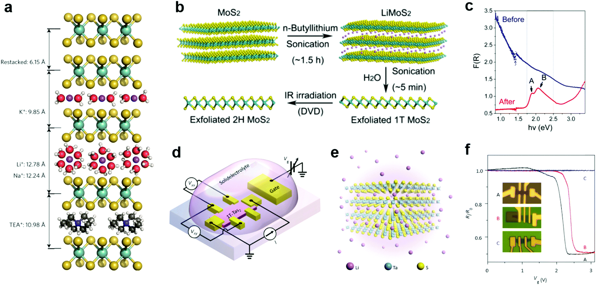 | ||
| Fig. 9 Intercalation modulation of MXs: (a) intercalation of MoS2 by alkali ions (Li+, Na+, K+) with solvent molecules, and by TEA+, reprinted with permission from ref. 193, Copyright 2015 Nature Publishing group. (b) Sonication assisted exfoliation of MoS2 in the 1T phase and IR irradiation assisted restoration; (c) the resulting reflectance spectral change, reprinted with permission from ref. 200, Copyright 2015 American Chemical Society. (d) The electrochemical setup and (e) the illustration of Li intercalation in TaS2; (f) patterned control of Li+ intercalation into devices and the resulting gate modulation characteristics, reprinted with permission from ref. 40, Copyright 2015 Nature Publishing group. | ||
In the liquid phase exfoliation, the host materials are simply soaked in H+ or alkali+-containing media such as acids199 and organo-alkali compounds.190 The intercalation is driven by external sonication200 or electrochemical potential bias.198 A typical example is illustrated in Fig. 9b, in which 1T-MoS2 is fabricated following the successive sonication of MoS2 in n-butyllithium (n-Bu-Li) solution and water.200 Due to the strong electron donation from intercalated ions, the obtained MoS2 structure was distorted from the starting host lattice to stabilize the electronic arrangement. The resulting metallic 1T phase is highly conductive for supercapacitors,193 and exhibits excellent catalytic activity for HER, yielding a low Tafel slope of 40 mV dec−1.201 It should be mentioned that such lattice distortion after intercalation could, however, be feasibly recovered to the 2H phase using thermal annealing (>300 °C)202 or laser-induced healing processes,200 thus restoring the semiconductor properties (indicated by the reflectance spectra and exciton features in Fig. 9c). Recently, the H+ intercalated MoS2 in acid environments was demonstrated to significantly improve the HER activity with considerable stability in neutral and alkaline electrolytes, rendering the potential for full water splitting.199
To control the extent of intercalation, Zhang et al. applied an electrochemical setup with high-yield exfoliation efficiency for transition metal dichalcogenides (MoS2, WS2, TiS2, TaS2 and ZrS2).191 The method has been also applied to NbSe2.203 Using Li metal foil as the ion source and layered MXs as the cathode, the extent of intercalation was monitored in the electrochemical cell and well-controlled during the discharge process. The electrochemical cell setup for ion intercalation was later reassembled on microscale devices using side gate structures, with ion containing electrolytes as the intercalation source, as illustrated in Fig. 9d.40 The electrical performances of host 2D materials were monitored in situ and controlled during the gate bias driven intercalation.40,195,203 In Li intercalated 1T-TaS2 (Fig. 9e), Yu et al. observed the alteration of charge-ordered states and 5 orders of magnitude change in resistance with multiple phase transitions from Mott-insulator to metal, and further to superconductor at low temperature.40 By a patterned PMMA blocking layer, the selective area intercalation and modulation to material performances was demonstrated, as indicated in Fig. 9f, thereby opening up possibilities for gate-controlled intercalation in devices.
Taking advantage of the giant modulation of the electronic states of the 2D MXs by ion intercalation and their non-volatile characteristics, the ion intercalated MXs have been utilized in constructing neuromorphic devices,18,204 rendering rich synapse functions including spike-dependent logic operation/modulation, multiplicative neural coding and gain modulation.204 The adsorption and intercalation enable the short-term and long-term memory functions in the synapses.18 By preparing holey structures in the basal planes of 2D MXs, the ion diffusion vertical to the vdW layer structure could be tailored to mimic the ion diffusion in bio-systems, and thus the related bio-functions.18 Notably, the H+ and Li+ intercalation were also found to be possible at the interspace between the 2D material and the substrates, enabling the intercalation modulation to functional devices based on monolayer MXs.205
5.2 Zerovalent intercalation of heavy metal elements
In addition to the light elements, heavy elements like transition metals (Cu, Co, etc.) can also be intercalated into 2D MXs.187,188,206,207 The lesser reactivity of these guest species allows distinct zerovalent intercalation with no charge interaction between the intercalant and host lattice, thus avoiding the lattice disruption usually observed in ion interacted 2D MXs.188 This allows the high concentration superstoichiometric intercalation of foreign species in the host lattice of 2D MXs, which not only modulates their electrical doping and optical properties, but also renders a series of surprising and unusual phenomena including ferromagnetic moments,208 charge density waves and superconductivity.209In 2012, Koski et al. successfully realized the high concentration zerovalent intercalation of Cu into the layered Bi2Se3, a well-known topological insulator with large interlayer space (9.53 Å), using a disproportionate redox reaction of monovalent copper (2Cu+(aq) ↔ Cu2+(aq) + Cu0) that leaves zerovalent Cu intercalated in the interlayer space, as indicated in Fig. 10a.206 The intercalated concentration of Cu in Bi2Se3 nanoribbons reached 60% of the host lattice atoms, leading to the stoichiometry of Cu7.5Bi2Se3, which is considerably higher than the usual cases of ion intercalation by electrochemical methods. It was later demonstrated that the method could be extended to other host materials210 including Bi2Te3, In2Se3, GaSe, Sb2Te3, MoO3, and using other guest atoms like Ag, Au, Co, Fe, In, Ni, Pd and Sn.188 The features of zerovalent intercalation and superstoichiometric intercalation are clearly evidenced from the composition analysis displayed in Fig. 10c.188 In particular, substantial electron doping from the superstoichiometric intercalation resulted in a peculiar enhancement of the optical transmission of the host lattice by causing the huge Burstein–Moss shift in the bandgap, at a much larger scale than degenerate doping.211 Recently, a vapour phase intercalation of Cu in Bi2Se3 and Bi2Te3 was demonstrated using Cu nanocrystals as the source, where high concentration Cu (>35%) incorporation was found to lead to the cation exchange of Cu2−xSe.212 This is likely a result of the corrupted thermal stability of the MXs lattice at a higher temperature (250–450 °C).
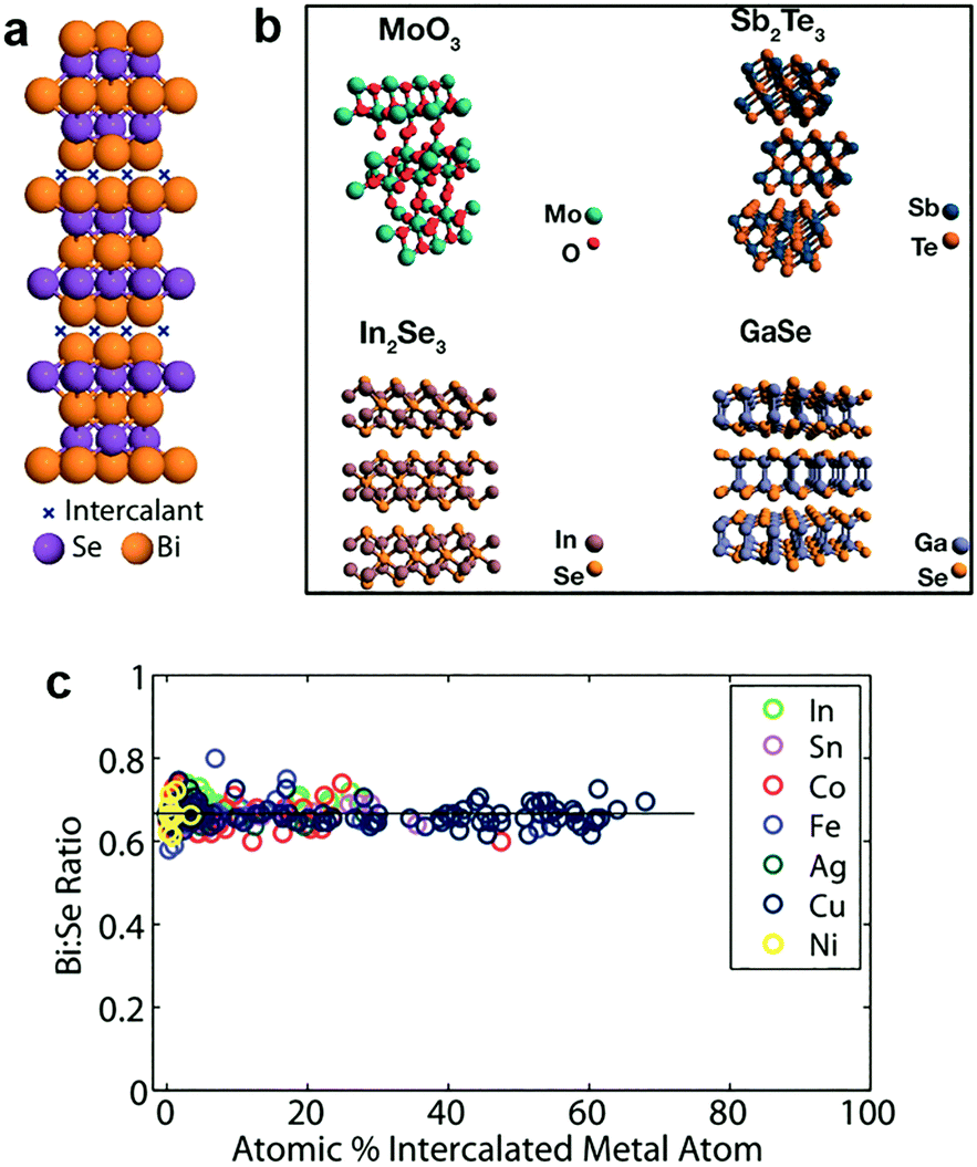 | ||
| Fig. 10 Zerovalent intercalation of MXs: (a) Cu intercalation in Bi2Se3, (b) 2D TMDs available for zerovalent intercalation, reprinted with permission from ref. 188 and 210 Copyright 2012, 2014 American Chemical Society. (c) Bi:Se composition under superstoichiometric intercalation of In, Sn, Co, Fe, Ag, Cu, Ni elements, reprinted with permission from ref. 188 Copyright 2012 American Chemical Society. | ||
To control the intercalation concentration of atomic species, Zhang et al. further devised an electrochemical setup using Bi2Se3 as the working electrode (WE) and Cu foil as the counter electrodes (CE).198 The copper intercalation was found to occur at a well-defined potential plateau of ∼17 mV over CE, thereby enabling the accurate control of Cu incorporation of up to 57% into the host lattice through a coulometric strategy. Another meaningful advance to the zerovalent intercalation was made through the stepwise combination of a disproportionate redox reaction, hydrazine reduction or carbonyl decomposition, by which Koski et al. were able to introduce multiple zerovalent species (Co/Ni, Cu/Ni, Fe/Ni, etc.) into the Bi2Se3 nanoribbons.207 The prepared materials exhibited a variety of superlattice diffraction patterns from the ordered structures of intercalated species and charge density wave characteristics. The versatile atom species and their combination in such multiple intercalations will undoubtedly create enormous opportunities for the creation of novel materials with intriguing optical and electrical properties.
The zerovalent intercalation also enabled the construction of various functional devices. In SnS2, using the disproportionate redox reaction of Cu and Co species, p-type and half-metallic doping were recently achieved at the atomic bilayer thickness, as schematically illustrated in Fig. 11a.187 This in principle allowed the facile construction of metal–semiconductor and semiconductor p–n junctions. To this end, a selective-area patterning technique was developed by using Zn and Al as the protective mask during the intercalation doping processes (Fig. 11b). The versatile electrical properties of intercalation doped SnS2 are particularly encouraging for constructing practical applications based on in-plane heterostructures, e.g., high-performance transistors of ultralow sub-threshold swing (SS ∼ 60 mV dec−1), and p–n junctions with high on–off ratios. Further, the metallic contact is also critical for the exploration of various interesting properties including ferromagnetism and superconductivity.187 It should be noted that, for disproportionate redox reaction, the solvent chosen was possibly critical for the zerovalent intercalation, since for the same host lattice of SnS2, acetone solvent was found to be more likely to result in zerovalent intercalation,187 while anhydrous methanol tended to minimize the disproportionation redox reaction and yield cation exchanged products, i.e. Cu2SnS3.213
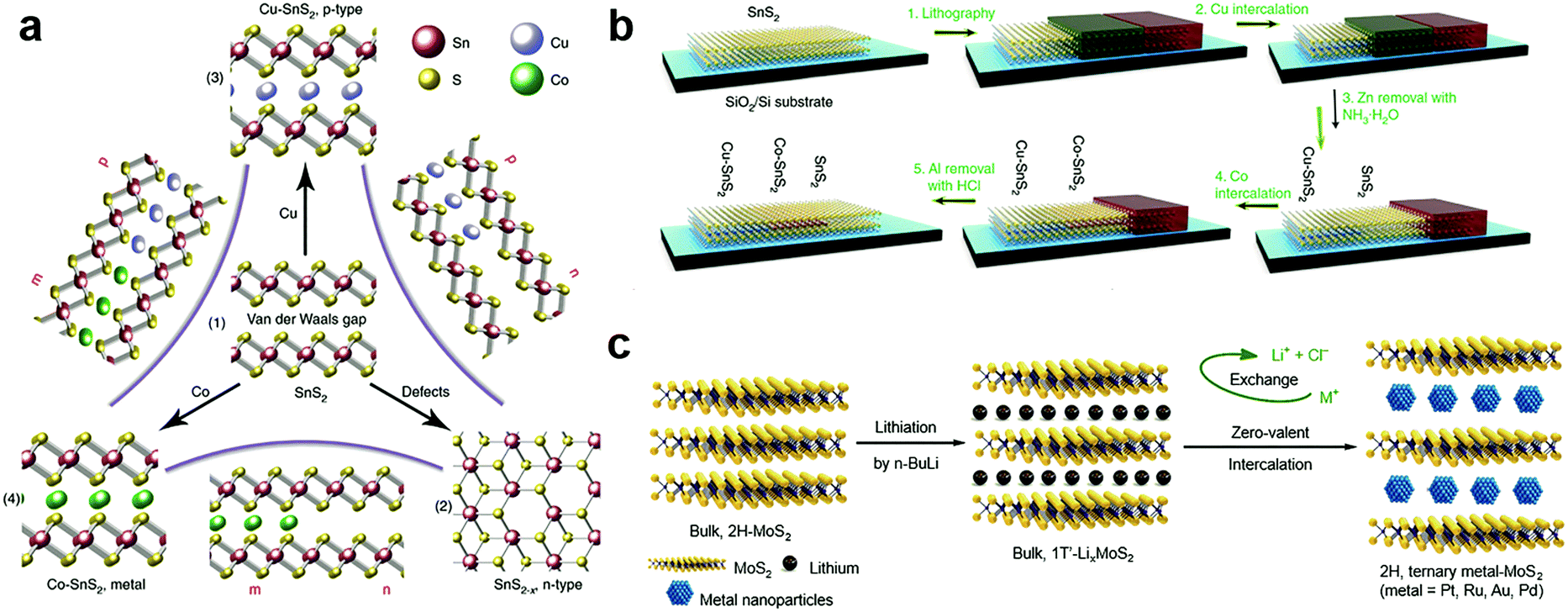 | ||
| Fig. 11 Zerovalent interaction of MXs: (a) the zerovalent intercalation of SnS2 by Cu and Co, enabling facile p, n, and metallic modulation. (b) The illustration of mask protected intercalation for fabricating lateral junctions, reprinted with permission from ref. 187, Copyright 2018 Nature Publishing group. (c) The lithium intercalation assisted zerovalent intercalation of noble metals into MoS2, reprinted with permission from ref. 36, Copyright 2017 Nature Publishing group. | ||
The zerovalent intercalation of noble metals in MXs was also demonstrated as possible. Recently, using highly reductive 1T′ LixMoS2 as the starting material, Chen et al. successfully realized the intercalation of Pt, Ru, Au and Pd in MoS2 through an in situ reduction of those metal ions, as illustrated in Fig. 11c.36 The process was performed in a non-aqueous solution, in which the Li+ intercalation enlarged the vdW gap in 1T′ LixMoS2, allowing the diffusion of high-valent state metal-containing ions (PbCl62−, Ru3+, AuCl4−, Pb2+) into the interlayer space. When following by an in situ reduction of their zerovalent state, the noble metal particles were precipitated in the interlayer space. Notably, after ion exchange that leached out Li+ and Cl−, the zerovalent intercalated MoS2 was restored to its stable 2H structure, where, because of the interlayer confinement, the resulted noble metal clusters were kept at ∼2 nm and were highly active for the HER. The encapsulation of noble metal clusters in MoS2 was particularly desirable for the long-term stability in catalytic reactions by preventing poisoning species from accessing to the catalyst surface; thus it opened a new avenue for catalyst engineering by intercalation chemistry.36
In addition to the above-mentioned ions and elemental atoms with small sizes, larger molecules could also be used as the intercalants. Though they were initially explored for liquid phase exfoliation purposes, there has been increasing attention to the modulation of application performances of MXs.214,215 For example, Wan et al. prepared a multiple molecule intercalated TiS2/[(hexylammonium)x(H2O)y(DMSO)z] through successive electrochemical intercalation and ion exchange processes,216 reaching a promising thermoelectric figure of merit, ZT, of 0.28 at 373 K. With the enormous choices of organic molecules and their functional groups, the organic molecules as intercalants will for sure promote the discovery of new intercalation systems and engineering of their functions.
6. Electrostatic doping
Due to their ultrathin nature, thin flakes of 2D materials are particularly susceptible to external field effects. This characteristic leads to the electrostatic doping strategy for tailoring the carrier doping concentration and polarity in semiconductor 2D MXs.54 Since the strategy is based on capacitance coupling between the external gate and 2D channels, it is known to exhibit ubiquitous advantages in non-destructive, reversible, stable and durable regulation and industrial availability.12 In the past, numerous gate modulation configurations using high-k dielectrics (HfO2, ZrO2, etc.),44,217 ionic liquids or gels,39,218–221 and ferroelectrics,222,223 have been explored, while the gate configuration has also been devised into floating224,225 and half-floating226 to accommodate multiple-function integration. Here, in accordance with the previously discussed doping strategies, we only focus on those non-volatile electrostatic doping configurations so that the electrical doping effect is efficiently maintained after withdrawing the gate bias, i.e. by using the floating gate configuration224–230 and ferroelectric dielectrics.222,223,231–2346.1 Floating gate modulation
Tunnelling diodes with metal–insulator–semiconductor (MIS) structures, in which the electrons or holes would tunnel through the insulating layer and form a circuit, provide the inspiration of a special electrostatic doping structure to 2D materials with a floating gate.235 When driven by a large potential bias, the free charges would tunnel through the insulating layer to the floating gate, where the charges are trapped by another dielectric layer.224 As a result, the trapped charges in the floating gate continuously modulate the electrical conductivity in the semiconductor channel via capacitance coupling.54 For 2D materials, a unique merit is that the semiconductor channel, insulating tunnelling layer, and the floating gate layer can all be selected from existing 2D materials with semiconducting, insulating and metallic properties.236 Their 2D nature further enables direct device fabrication via vdW stacking.237According to the driving gate biases, the floating gate configurations are further classified into three-terminal16 and two-terminal227,228 structures with or without a separate control gate. Fig. 12a illustrates a typical three-terminal structure where the floating gate is inserted in a MoSe2 field-effect transistor.238 To fabricate the floating gate device, graphene, h-BN and MoSe2 were successively transferred above the SiO2/Si substrate, in which h-BN was taken as the tunnelling barrier layer while graphene acted as the floating gate. The charge trapping and modulation of channel conductance could be identified from the measured transfer curves, as indicated in Fig. 12b. The tunnelling of free charges into the floating graphene layer caused dramatic modulation of the threshold voltage of the MoSe2 layer, which resulted in the appearance of two electrical conductance states, namely the ON and OFF states. Due to the persistent characteristics of the trapped charges, the ON and OFF states were non-volatile and they can be used in memory devices.224,227,238 Under opposite gate biases, the electrical conductance in the semiconductor channel can be written (programmed) or erased.
 | ||
| Fig. 12 Floating gate modulation of MXs: (a) the typical floating gate structure is integrated into a transistor; (b) the resulting hysteresis under control gate modulation due to (c) charge trapping of the floating gate under control gate bias, reprinted with permission from ref. 238, Copyright 2017 American Physical Society. (d) Semi-floating gate configuration and (e) the resulting rectification characteristics in the WSe2 transistor, reprinted with permission from ref. 243, Copyright 2017 Nature Publishing group. (f) A semi-floating gate integrated in parallel with a vertical PN junction, reprinted with permission from ref. 226, Copyright 2018 Nature Publishing group. (g)–(i) The typical two terminal floating gate configuration and its current–voltage and memory characteristics, reprinted with permission from ref. 228, Copyright 2016 Nature Publishing group. | ||
The operating principle of the floating gate device is explained in Fig. 12c from the band diagrams.238 Under the positive control gate bias, the majority of electron carriers in MoSe2 are forced to tunnel into the intermediate graphene layer through Fowler–Nordheim (FN) tunnelling, in which the tunnelling barrier is lowered by the strong external electric field.227 When electrons are trapped in the floating gate, the semiconductor channel is p-doped with the same amount of holes due to the charge compensation rule. Conversely, the trapped charges can be repelled into the semiconductor channel under negative gate biases. Thus, the doping concentration and polarity in semiconductor MXs can be feasibly tuned by choosing the magnitude and duration of the gate bias.16 Because the insulator barrier surrounds the floating gate layer, the trapped charges can persist for non-volatile doping for years, while the proper bandgap (1–2 eV) of semiconductor MXs (MoS2, MoSe2, WSe2, etc.) enables large on–off ratios (103–105) in memory devices.16 For a higher doping level or memory ratio, the thickness of the charge trapping layer or tunnelling barriers could be reduced to allow more charge trapping,16 while a too thin dielectric layer would cause leaking current and poor retention characteristics.239 In addition to the conventional high-k dielectrics and 2D h-BN, polymer and SAM insulators such as PVP,240 pV3D3229 and alkyl chain SAMs241 have also been explored as the tunnelling insulators in floating devices. This could potentially relieve the surface stability issue of MXs during the high-temperature processing of high-k oxides and the scalable issue when using the mechanically exfoliated and transferred h-BN.
Notably, the floating gate induced electrical doping and its persistent characteristics have been applied to other functional devices beyond memories. By applying the floating gate structure to phototransistors, Hu et al. were able to remarkably suppress the dark current in MoS2 and WS2 channels, thereby enhancing the photodetectivity to 3.5 × 10¹¹ Jones while maintaining a high responsivity over 103 A W−1.242 However, the persistent charge trapping characteristics in floating gate configuration generally resulted in the persistent photoconductance (PPC) effect in photodetection that was usually refreshed using reversed gate pulses.
Similar to other doping methods, the floating gate structure could also be used for selective region doping, e.g. by using a partially stacked or underlapped floating gate. A typical structure is illustrated in Fig. 12d, by which Zhang et al. realized a semi-floating gate-controlled transistor with rectification characteristics.243 Due to the charge trapping in the underlap floating graphene layer, the doping concentration and polarity in the WSe2 channel were partially modulated beneath the drain electrode. With the inherent p-type conduction in WSe2, a PN junction was realized by applying a negative gate pulse, which induced positive charge trapping into the floating gate and n-type conductance in the above WSe2 channel. The resulting homojunction displayed apparent rectification (Fig. 12e), photovoltaic conversion and long retention characteristics (>103 s). Similarly, non-volatile PNP junctions were also realized with the middle part of the semiconductor channel coupled with the floating gate.244 Further, an ingenious parallel integration of the semi-floating gate (MoS2/h-BN/HfS2) with a vertical WSe2/MoS2 pn junction (Fig. 12f), which exhibited fast charge injection yet low reverse current leakage, was recently reported to enable both tuneable charge persistency and ultrafast operation speed on a nanosecond scale.226 It is apparent that the feasible but versatile integration configurations of floating gates in devices have greatly promoted the brilliant development of multifunctional devices based on MXs.
Recently, two-terminal floating gate devices were also invented to simplify the charge trapping operation through the control gate and the reliance on gate blocking insulators. As shown in Fig. 12g, the devices exhibited only source and drain terminals with a floating gate beneath them.228 By reducing the thickness of the tunnelling insulator (<10 nm), the applied source-drain potential bias was sufficient to induce charge injection to the floating layer. The charge trapping caused a large hysteresis and well-defined ON/OFF states in a simple cycle of current–voltage sweep (Fig. 12h). This characteristic enabled a two-terminal operation of memory devices, in which the write, read, erase, read were respectively achieved by separate source–drain biases denoted as (i), (ii), (iii), (iv) in Fig. 12h. Such two terminal devices not only exhibited stable operation voltages but could also maintain high on/off ratios (>104) (Fig. 12i), long retentivity (>104 s), stable endurance (>105 cycles) and multilevel capacity. The absence of a rigid dielectric blocking layer made it stretchable up to a strain of 19% without deterioration of electrical performances. When combined with a large area MoS2 film and ALD grown dielectrics, a flexible memory array and 6-levels of discriminate operation were later achieved,227 implying the great potential of such two-terminal floating gate devices in wearable electronics and neuromorphic memories.
6.2 Ferroelectric gate
Ferroelectric materials exhibit spontaneous polarization that can be maintained even in the absence of an external electric field. Particularly, the polarization can be reversed by applying external poling voltages. The rewritable and persistent characteristics of ferroelectric polarization and their inherent high-k dielectric nature have attracted much interest in non-volatile memories, transducers, capacitors, and transistors.245 Recently, ferroelectric materials have been used to couple with 2D semiconductors for electrostatic modulation of the doping status of 2D materials.245 The combination has led to novel memory devices222,231,246–248 and dramatic improvements to the photodetection performances in detectors.223,249Lead zirconium titanate (Pb(Zr,Ti)O3, PZT) has been the most studied ferroelectric material with high remnant polarization (20–80 μC cm−2).248 The value is orders of magnitude larger than the charge density induced by capacitance coupling in field-effect transistors, which is typically 0.345 μC cm−2 for 100 nm SiO2 under a gate bias of 10 V. The large remnant polarization enabled the dramatic modulation of the doping concentration and polarity of 2D materials by simple ferroelectric polarization.222,231,232,246,250–252 Due to the limitation in preparing high quality PZT films, i.e. high temperature, the integration of 2D MXs was generally realized by transferring and placing them on top of PZT substrates.222,231,248,251 A typical structure is illustrated in Fig. 13a, in which the semiconductor channel worked together with the back gate as the two poling electrodes.248 The polarization loop measured at varied poling voltages indicated tailorable remnant polarization in the ferroelectric layer under appreciably low operation voltages below 4 V (Fig. 13b). By using such bottom gated ferroelectric coupling, Lipatov et al. successfully reversed the doping polarity of MoS2 to p-type.222 Their device structure and ferroelectric polarization effects are indicated in Fig. 13c and d. The persistent ferroelectric modulation of MoS2 was implied by the electrical conductance change of MoS2 5 min after resetting the gate bias (Vg) to 0 V (Fig. 13d). It was found that the ferroelectric polarization could be depolarized by shedding light on the MoS2 area, thus allowing feasible writing and erasing operations in memories using the combined optical and electrical methods indicated in Fig. 13e. It should be noted that the retention characteristics were found to be related to the surface roughness of the ferroelectrics,248 and also the ambient environments,231 where both interfacial contaminants and humidity were prone to screen out the polarization.
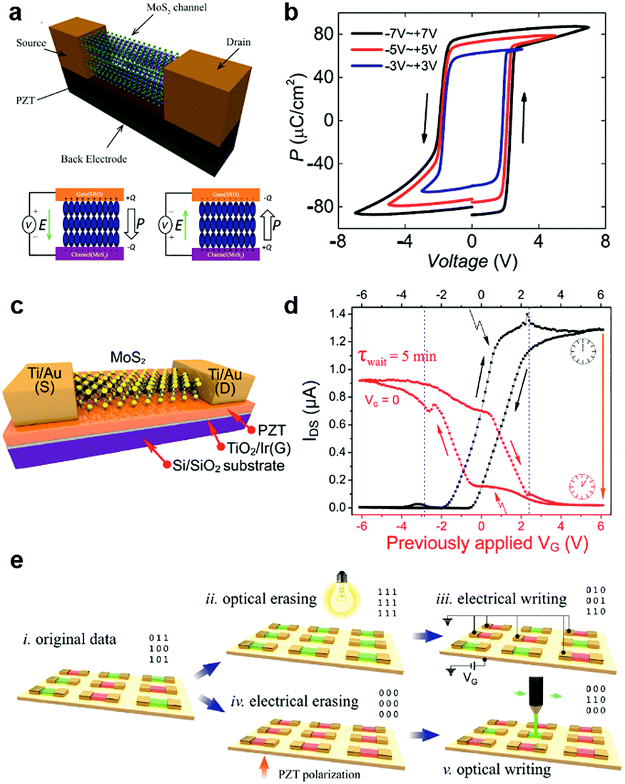 | ||
| Fig. 13 Ferroelectric doping of MXs with PZT at the bottom: (a) the typical configuration of ferroelectric transistor with 2D MoSe2 placed on top of ferroelectrics, and (b) the typical polarization characteristic of PZT ferroelectrics, reprinted with permission from ref. 248, Copyright 2017 American Physical Society. (c) MoS2 ferroelectric transistor and (d) the polarization induced conductance change in MoS2, (e) the potential write and erase procedures that combines optical and electrical operation, reprinted with permission from ref. 222, Copyright 2015 American Chemical Society. | ||
Poly(vinylidene fluoride-trifluoroethylene), abbreviated as p(VDF-TrFE), is a commonly used ferroelectric polymer that can be processed through spin-coating methods at mild temperatures.223,233,234 The spontaneous polarization stems from the large electronegativity difference between the H and F atoms. Their configuration and polarization are tuned by the external electric field. The typical remnant polarization is usually ∼8 μC cm−2.253 Due to the ease of processing polymers, they were adapted to 2D materials generally using the top-gate configuration, as indicated in Fig. 14a.252 In a MoSe2 based transistor with 300 nm thick p(VDF-TrFE), a large hysteresis and memory window were observed during a back gate voltage sweep (Fig. 14b). The leakage current through the ferroelectric gate remained small (<1 nA) during the sweep, but showed peaks near the coercive field of the ferroelectric polymer. The well-defined hysteresis and voltage window for conductance modulation, and the high on–off ratio >105 rendered excellent endurance characteristics of the device as memory, as indicated in Fig. 14c. This suggested the excellent persistence of the ferroelectric polarization induced doping in 2D materials. Notably, increasing the thickness of MoSe2 in the device reduced the memory window and the on–off ratio due to the charge screening in MoSe2 or the depolarization effect in the ferroelectric polymer.252 The uncertain change in the contact resistance in the devices may also lead to such decreased on–off ratio, as discussed by Lin et al.254
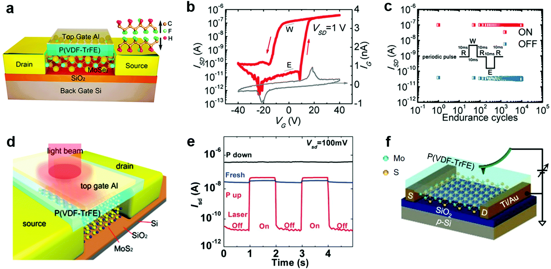 | ||
| Fig. 14 Ferroelectric doping of MXs using the top gate configuration: (a) the typical configuration of the MoSe2 based ferroelectric transistor with Al as the top gate; (b) the measured hysteresis and (c) retention characteristics for memory, reprinted with permission from ref. 252, Copyright 2017 IOP Publishing group. (d) Ferroelectric phototransistor and (e) its photodetection performance under different polarization states, reprinted with permission from ref. 223, Copyright 2015 Wiley-VCH. (f) Schematic of the AFM probe setup for the selective area polarization of ferroelectric polymer on MoS2 channel, reprinted with permission from ref. 233, Copyright 2017 American Physical Society. | ||
The ferroelectric polymer coupling to 2D MXs has also been utilized to boost the photodetection performances in detectors. By using a patterned Al gate electrode on top of the p(VDF-TrFE) layer displayed in Fig. 14d,223 Hu et al. successfully achieved the dramatic suppression of the photodetection dark current by almost 3 orders in a MoS2 detector polarized to the Pup state, as indicated in Fig. 14e. Compared to the fresh device, the photocurrent also showed improvement after the ferroelectric polarization. The hybrid structure thus rendered an overall lift of the photodetection performance compared to bare MoS2, yielding high responsivity (>2500 A W−1), fast response speed (<2 ms), as well excellent detectivity up to 2.2 × 10¹² Jones. In particular, the strong polarization field imposed on MoS2 even led to the modulation of its electronic band structure, enabling near-infrared photodetection at the considerably longer wavelengths than normally allowed.223 The structure was recently successfully extended to MoTe2,255 WSe2,234 In2Se3,249 making possible the optimization of photodetection via facile ferroelectric polarization.
Through a careful analysis of the carrier mobility in p(VDF-TrFE) coupled MoS2 by correcting the free carrier density, Xiao et al. found that the integration of the ferroelectric polymer interface does not impose additional scattering or degrade the inherent carrier mobility of 2D MoS2.233 On the other hand, the ferroelectric polarization-induced doping modulation of MXs could be utilized to optimize the carrier mobility in 2D MXs. For example, Wang et al. found that after coating p(VDF-TrFE-CFE), the hole mobility in WSe2 was improved from 27 to 170 cm2 V−1 s−1 at room temperature,234 which could be attributed to both the improved dielectric and free carrier screening of Coulomb scattering.233 In MoS2, a superior effective field-effect electron mobility of 625 cm2 V−1 s−1 was even achieved when MoS2 was placed on top of the 150 nm thick p(VDF-TrFE). The high carrier mobility in 2D MXs helped to decrease the sub-threshold swing in transistors, which is desired for low power devices.234 To this end, the negative capacitance effect in ferroelectric materials has also been explored. An example was recently reported by Wang et al., in which an ultralow SS of 24 mV dec−1 was demonstrated in p(VDF-TrFE) coupled MoS2.232 The crystallinity of the ferroelectric polymer was found to be critical to optimize the SS below 60 mV dec−1 since it determines the polarization intensity and switching characteristics. This, however, poses a challenge to the integration of ultrathin ferroelectric polymers.
In addition to the top gate or bottom gate polarization, the ferroelectric materials can also be polarized by using scanning probes. As indicated in Fig. 14f, an AFM probe with an applied voltage was used to polarize the ferroelectric polymer on top of MoS2.233 The selective area scanning allowed patterned modulation of the electrical conductance in MoS2, and further, the facile preparation of Schottky junctions across the channel. Though time-consuming, the method is still a good choice for understanding the effect of the ferroelectric modulation of 2D MXs, especially in terms of local effects, e.g. during the construction of planar or vertical p–n junctions.
7. Conclusion and outlook
In summary, we have given in the above an inclusive review of the strategies and recent advances towards the doping engineering and functionalization of 2D MXs. Compared to the mainstream Si, III–V semiconductors, the tailorable doping engineering remains to be developed and maturated for the solid foundation of practical applications in transistors, memories, detectors and even electrochemical devices. At present, by using substitutional doping, surface charge transfer doping, intercalation and electrostatic doping, one could achieve both non-degenerate and degenerate modulation of 2D MXs. This not only enabled the realization of widely tuned semiconductor properties but also allowed the appearance of metallic behaviours and phase transition under the intensive charge injection. However, there are still challenges mainly arising from the demand of addressing the precisely controlled dopant incorporation, activation and long-term stability issues, and also the resulted function performances. More attention should be therefore paid on clarifying the dopant interaction with various 2D MXs in substitutional doping, charge transfer doping and intercalation doping, thus to maintain the crystalline integrity of host materials.In Table 3, we finally summarize the main strategies and the related doping sources available for functionalization of 2D MXs. Though each strategy may have its own limitations, enormous new properties and functions have been enabled in the past by such doping engineering, which greatly promoted the wealthy evolving of various kinds of functional devices. Moving forward, optimizing existing or finding new dopant sources is still important to improve the performance and enrich their application functions. As a non-destructive modulation method, the electrostatic doping has emerged as a convenient method to tune the electrical performances of 2D MXs. The facile construction of patterned floating gate or ferroelectric coupling is going to allow more and more sophisticated doping control of 2D MXs with synergistic functions integrated. One can therefore clearly foresee the wealthy potential of 2D MXs based on the increasingly developed doping processes with convenient, stable, flexible, and precise characteristics, by which intriguing multifunctional devices that integrate two or more functions can thrive.
| Doping strategy | Doping sources | Functions |
|---|---|---|
| Substitution | Cation: Re, Nb, Zn, W, Mo, Fe, Cr, Mn, Fe, V, Ni | PN diode, phase transition, ferromagnetism, photodetector, transistor |
| Anion: Se, S, Te, O, P, N, H, Cl | ||
| Charge transfer | Gaseous: O2, H2O, NO2 | PN diode, chemical & biosensor, transistor, photodetector, logic devices |
| Metals based: Ti4+, B3+, Al3+, Sn4+, Au3+(Au), K+(K), Ag, Pd, Pt, Sc, Y, Zn, Ca2N, MoO3, WO3(WOx), ATO, Cs2CO3 | ||
| Organic: OTS, APTMS, FOTS, BV, Pc, F4TCNQ, R6G, Co6Se8(PEt3)6, PPh3 | ||
| Intercalation | Ions: H+, Li+, Na+, K+, NH4+ | Exfoliation, HER, capacitor, phase transition, transistor, PN diodes |
| Atoms: Cu, Co, Ag, Au, Fe, In, Ni, Pd, Sn, P | ||
| Electrostatic | Floating gate by Gr, BP, MoS2, Au, Ag, Co, Al, HfO2, TiO2 | Memories, PN diodes, photodetectors, transistors, logic devices |
| Ferroelectric gate: the remnant polarization electric field in PZT, P(VDF-TrFE) | ||
Conflicts of interest
There are no conflicts to declare.Acknowledgements
This work was supported by National Natural Science Foundation of China (Grant No. 91622117, 51472097, and 51727809), National Key Research and Development Program of “Strategic Advanced Electronic Materials” (Grant No. 2016YFB0401100), and the Fundamental Research Funds for the Central University (Grant No. 2017KFKJXX007 and 2015ZDTD038). The authors are indebted for the kind permission from the corresponding publishers/authors to reproduce their materials, especially figures, used in this article.References
- H. Schmidt, F. Giustiniano and G. Eda, Chem. Soc. Rev., 2015, 44, 7715–7736 RSC.
- D. A. Bandurin, A. V. Tyurnina, G. L. Yu, A. Mishchenko, V. Zolyomi, S. V. Morozov, R. K. Kumar, R. V. Gorbachev, Z. R. Kudrynskyi, S. Pezzini, Z. D. Kovalyuk, U. Zeitler, K. S. Novoselov, A. Patane, L. Eaves, I. V. Grigorieva, V. I. Fal'ko, A. K. Geim and Y. Cao, Nat. Nanotechnol., 2017, 12, 223–227 CrossRef CAS PubMed.
- W. Jie, Z. Yang, G. Bai and J. Hao, Adv. Opt. Mater., 2018, 6, 1701296 CrossRef.
- K. F. Mak, K. He, C. Lee, G. H. Lee, J. Hone, T. F. Heinz and J. Shan, Nat. Mater., 2013, 12, 207–211 CrossRef CAS PubMed.
- M. M. Ugeda, A. J. Bradley, S.-F. Shi, F. H. da Jornada, Y. Zhang, D. Y. Qiu, W. Ruan, S.-K. Mo, Z. Hussain, Z.-X. Shen, F. Wang, S. G. Louie and M. F. Crommie, Nat. Mater., 2014, 13, 1091–1095 CrossRef CAS PubMed.
- K. F. Mak, K. He, J. Shan and T. F. Heinz, Nat. Nanotechnol., 2012, 7, 494–498 CrossRef CAS PubMed.
- B. W. Baugher, H. O. Churchill, Y. Yang and P. Jarillo-Herrero, Nat. Nanotechnol., 2014, 9, 262–267 CrossRef CAS PubMed.
- L. Li, L. Pi, H. Li and T. Zhai, Chin. Sci. Bull., 2017, 62, 3134–3153 CrossRef.
- F. W. Zhuge, Z. Zheng, P. Luo, L. Lv, Y. Huang, H. Q. Li and T. Y. Zhai, Adv. Mater. Technol., 2017, 2, 1700005 CrossRef.
- X. Zhou, X. Z. Hu, J. Yu, S. Y. Liu, Z. W. Shu, Q. Zhang, H. Q. Li, Y. Ma, H. Xu and T. Y. Zhai, Adv. Funct. Mater., 2018, 28, 1706587 CrossRef.
- B. Radisavljevic, A. Radenovic, J. Brivio, V. Giacometti and A. Kis, Nat. Nanotechnol., 2011, 6, 147–150 CrossRef CAS PubMed.
- M. Chhowalla, D. Jena and H. Zhang, Nat. Rev. Mater., 2016, 1, 16052 CrossRef CAS.
- L. Li, W. Wang, Y. Chai, H. Li, M. Tian and T. Zhai, Adv. Funct. Mater., 2017, 27, 1701011 CrossRef.
- S. Yang, C. Jiang and S.-H. Wei, Appl. Phys. Rev., 2017, 4, 021304 Search PubMed.
- K. Kalantar-zadeh and J. Z. Ou, ACS Sens., 2016, 1, 5–16 CrossRef CAS.
- M. S. Choi, G. H. Lee, Y. J. Yu, D. Y. Lee, S. H. Lee, P. Kim, J. Hone and W. J. Yoo, Nat. Commun., 2013, 4, 1624 CrossRef PubMed.
- T. Carey, S. Cacovich, G. Divitini, J. Ren, A. Mansouri, J. M. Kim, C. Wang, C. Ducati, R. Sordan and F. Torrisi, Nat. Commun., 2017, 8, 1202 CrossRef PubMed.
- J. Zhu, Y. Yang, R. Jia, Z. Liang, W. Zhu, Z. U. Rehman, L. Bao, X. Zhang, Y. Cai, L. Song and R. Huang, Adv. Mater., 2018, 30, 1800195 CrossRef PubMed.
- V. Nicolosi, M. Chhowalla, M. G. Kanatzidis, M. S. Strano and J. N. Coleman, Science, 2013, 340, 1226419 CrossRef.
- D. Dumcenco, D. Ovchinnikov, K. Marinov, P. Lazic, M. Gibertini, N. Marzari, O. L. Sanchez, Y.-C. Kung, D. Krasnozhon, M.-W. Chen, S. Bertolazzi, P. Gillet, A. Fontcuberta i Morral, A. Radenovic and A. Kis, ACS Nano, 2015, 9, 4611–4620 CrossRef CAS PubMed.
- Y. Zhan, Z. Liu, S. Najmaei, P. M. Ajayan and J. Lou, Small, 2012, 8, 966–971 CrossRef CAS PubMed.
- Y. Chen, L. Gan, H. Li, Y. Ma and T. Zhai, Adv. Mater., 2017, 29, 1603550 CrossRef PubMed.
- W. Huang, L. Gan, H. Yang, N. Zhou, R. Wang, W. Wu, H. Li, Y. Ma, H. Zeng and T. Zhai, Adv. Funct. Mater., 2017, 27, 1702448 CrossRef.
- J. Zhou, J. Lin, X. Huang, Y. Zhou, Y. Chen, J. Xia, H. Wang, Y. Xie, H. Yu, J. Lei, D. Wu, F. Liu, Q. Fu, Q. Zeng, C.-H. Hsu, C. Yang, L. Lu, T. Yu, Z. Shen, H. Lin, B. I. Yakobson, Q. Liu, K. Suenaga, G. Liu and Z. Liu, Nature, 2018, 556, 355–359 CrossRef CAS PubMed.
- V. P. Pham and G. Y. Yeom, Adv. Mater., 2016, 28, 9024–9059 CrossRef CAS PubMed.
- Y. Ding, N. Zhou, L. Gan, X. Yan, R. Wu, I. H. Abidi, A. Waleed, J. Pan, X. Ou, Q. Zhang, M. Zhuang, P. Wang, X. Pan, Z. Fan, T. Zhai and Z. Luo, Nano Energy, 2018, 49, 200–208 CrossRef CAS.
- X. Zhou, X. Hu, S. Zhou, H. Song, Q. Zhang, L. Pi, L. Li, H. Li, J. Lu and T. Zhai, Adv. Mater., 2018, 30, 1703286 CrossRef PubMed.
- H. Yuan, H. Wang and Y. Cui, Acc. Chem. Res., 2015, 48, 81–90 CrossRef CAS PubMed.
- W. Wu, Q. Zhang, X. Zhou, L. Li, J. Su, F. Wang and T. Zhai, Nano Energy, 2018, 51, 45–53 CrossRef CAS.
- C. Y. Yan, L. Gan, X. Zhou, J. Guo, W. J. Huang, J. W. Huang, B. Jin, J. Xiong, T. Y. Zhai and Y. R. Li, Adv. Funct. Mater., 2017, 27, 1702918 CrossRef.
- M. Chhowalla, H. S. Shin, G. Eda, L. J. Li, K. P. Loh and H. Zhang, Nat. Chem., 2013, 5, 263–275 CrossRef PubMed.
- J. Suh, T. E. Park, D. Y. Lin, D. Fu, J. Park, H. J. Jung, Y. Chen, C. Ko, C. Jang, Y. Sun, R. Sinclair, J. Chang, S. Tongay and J. Wu, Nano Lett., 2014, 14, 6976–6982 CrossRef CAS PubMed.
- A. Nipane, D. Karmakar, N. Kaushik, S. Karande and S. Lodha, ACS Nano, 2016, 10, 2128–2137 CrossRef CAS PubMed.
- G. X. Bai, S. G. Yuan, Y. D. Zhao, Z. B. Yang, S. Y. Choi, Y. Chai, S. F. Yu, S. P. Lau and J. H. Hao, Adv. Mater., 2016, 28, 7472–7477 CrossRef CAS PubMed.
- M. Amani, D. H. Lien, D. Kiriya, J. Xiao, A. Azcatl, J. Noh, S. R. Madhvapathy, R. Addou, S. Kc, M. Dubey, K. Cho, R. M. Wallace, S. C. Lee, J. H. He, J. W. Ager 3rd, X. Zhang, E. Yablonovitch and A. Javey, Science, 2015, 350, 1065–1068 CrossRef CAS PubMed.
- Z. Chen, K. Leng, X. Zhao, S. Malkhandi, W. Tang, B. Tian, L. Dong, L. Zheng, M. Lin, B. S. Yeo and K. P. Loh, Nat. Commun., 2017, 8, 14548 CrossRef CAS PubMed.
- G. L. Liu, A. W. Robertson, M. M. J. Li, W. C. H. Kuo, M. T. Darby, M. H. Muhieddine, Y. C. Lin, K. Suenaga, M. Stamatakis, J. H. Warner and S. C. E. Tsang, Nat. Chem., 2017, 9, 810–816 CrossRef CAS PubMed.
- C. Li, Y. Liu, Z. Zhou, H. Ju, D. Li, Y. Guo, X. Wu, H. Li and T. Zhai, Adv. Energy Mater., 2018 DOI:10.1002/aenm.201801775.
- Y. Wang, J. Xiao, H. Y. Zhu, Y. Li, Y. Alsaid, K. Y. Fong, Y. Zhou, S. Q. Wang, W. Shi, Y. Wang, A. Zettl, E. J. Reed and X. Zhang, Nature, 2017, 550, 487–491 CrossRef CAS PubMed.
- Y. J. Yu, F. Y. Yang, X. F. Lu, Y. J. Yan, Y. H. Cho, L. G. Ma, X. H. Niu, S. Kim, Y. W. Son, D. L. Feng, S. Y. Li, S. W. Cheong, X. H. Chen and Y. B. Zhang, Nat. Nanotechnol., 2015, 10, 270–276 CrossRef CAS PubMed.
- D. Yang, X. Hu, M. Zhuang, Y. Ding, S. Zhou, A. Li, Y. Yu, H. Li, Z. Luo, L. Gan and T. Zhai, Adv. Funct. Mater., 2018, 28, 1800785 CrossRef.
- H. Schmidt, F. Giustiniano and G. Eda, Chem. Soc. Rev., 2015, 44, 7715–7736 RSC.
- Y. D. Zhao, K. Xu, F. Pan, C. J. Zhou, F. C. Zhou and Y. Chai, Adv. Funct. Mater., 2017, 27, 1603484 CrossRef.
- F. Wang, Z. X. Wang, C. Jiang, L. Yin, R. Q. Cheng, X. Y. Zhan, K. Xu, F. M. Wang, Y. Zhang and J. He, Small, 2017, 13, 1604298 CrossRef PubMed.
- B. Li, T. Xing, M. Z. Zhong, L. Huang, N. Lei, J. Zhang, J. B. Li and Z. M. Wei, Nat. Commun., 2017, 8, 1958 CrossRef PubMed.
- V. Kochat, A. Apte, J. A. Hachtel, H. Kumazoe, A. Krishnamoorthy, S. Susarla, J. C. Idrobo, F. Shimojo, P. Vashishta, R. Kalia, A. Nakano, C. S. Tiwary and P. M. Ajayan, Adv. Mater., 2017, 29, 1703754 CrossRef PubMed.
- J. R. Schaibley, H. Yu, G. Clark, P. Rivera, J. S. Ross, K. L. Seyler, W. Yao and X. Xu, Nat. Rev. Mater., 2016, 1, 16055 CrossRef CAS.
- M. A. Hughes, Y. Fedorenko, B. Gholipour, J. Yao, T.-H. Lee, R. M. Gwilliam, K. P. Homewood, S. Hinder, D. W. Hewak, S. R. Elliott and R. J. Curry, Nat. Commun., 2014, 5, 5346 CrossRef CAS PubMed.
- J. Suh, T. L. Tan, W. J. Zhao, J. Park, D. Y. Lin, T. E. Park, J. Kim, C. H. Jin, N. Saigal, S. Ghosh, Z. M. Wong, Y. B. Chen, F. Wang, W. Walukiewicz, G. Eda and J. Q. Wu, Nat. Commun., 2018, 9, 199 CrossRef PubMed.
- J. Gao, Y. D. Kim, L. B. Liang, J. C. Idrobo, P. Chow, J. W. Tan, B. C. Li, L. Li, B. G. Sumpter, T. M. Lu, V. Meunier, J. Hone and N. Koratkar, Adv. Mater., 2016, 28, 9735–9743 CrossRef CAS PubMed.
- X. Zhang, Z. Shao, X. Zhang, Y. He and J. Jie, Adv. Mater., 2016, 28, 10409–10442 CrossRef CAS PubMed.
- J. Y. Wan, S. D. Lacey, J. Q. Dai, W. Z. Bao, M. S. Fuhrer and L. B. Hu, Chem. Soc. Rev., 2016, 45, 6742–6765 RSC.
- Y. Jung, Y. Zhou and J. J. Cha, Inorg. Chem. Front., 2016, 3, 452–463 RSC.
- J. Wang, H. Fang, X. Wang, X. Chen, W. Lu and W. Hu, Small, 2017, 13, 1700894 CrossRef PubMed.
- A. Y. Lu, H. Zhu, J. Xiao, C. P. Chuu, Y. Han, M. H. Chiu, C. C. Cheng, C. W. Yang, K. H. Wei, Y. Yang, Y. Wang, D. Sokaras, D. Nordlund, P. Yang, D. A. Muller, M. Y. Chou, X. Zhang and L. J. Li, Nat. Nanotechnol., 2017, 12, 744–749 CrossRef CAS PubMed.
- L. Dong, J. Lou and V. B. Shenoy, ACS Nano, 2017, 11, 8242–8248 CrossRef CAS PubMed.
- J. Zhang, S. Jia, I. Kholmanov, L. Dong, D. Er, W. Chen, H. Guo, Z. Jin, V. B. Shenoy, L. Shi and J. Lou, ACS Nano, 2017, 11, 8192–8198 CrossRef CAS PubMed.
- W. Choi, N. Choudhary, G. H. Han, J. Park, D. Akinwande and Y. H. Lee, Mater. Today, 2017, 20, 116–130 CrossRef CAS.
- S. Wang, Y. Rong, Y. Fan, M. Pacios, H. Bhaskaran, K. He and J. H. Warner, Chem. Mater., 2014, 26, 6371–6379 CrossRef CAS.
- A. Govind Rajan, J. H. Warner, D. Blankschtein and M. S. Strano, ACS Nano, 2016, 10, 4330–4344 CrossRef CAS PubMed.
- K. Cho, M. Min, T. Y. Kim, H. Jeong, J. Pak, J. K. Kim, J. Jang, S. J. Yun, Y. H. Lee, W. K. Hong and T. Lee, ACS Nano, 2015, 9, 8044–8053 CrossRef CAS PubMed.
- D. M. Sim, M. Kim, S. Yim, M. J. Choi, J. Choi, S. Yoo and Y. S. Jung, ACS Nano, 2015, 9, 12115–12123 CrossRef CAS PubMed.
- Y. Meng, C. Ling, R. Xin, P. Wang, Y. Song, H. Bu, S. Gao, X. Wang, F. Song, J. Wang, X. Wang, B. Wang and G. Wang, NPJ Quant. Mater., 2017, 2, 16 CrossRef.
- X. Zhang, Q. Liao, S. Liu, Z. Kang, Z. Zhang, J. Du, F. Li, S. Zhang, J. Xiao, B. Liu, Y. Ou, X. Liu, L. Gu and Y. Zhang, Nat. Commun., 2017, 8, 15881 CrossRef CAS PubMed.
- S.-L. Li, K. Tsukagoshi, E. Orgiu and P. Samori, Chem. Soc. Rev., 2016, 45, 118–151 RSC.
- P. K. Chow, R. B. Jacobs-Gedrim, J. Gao, T.-M. Lu, B. Yu, H. Terrones and N. Koratkar, ACS Nano, 2015, 9, 1520–1527 CrossRef CAS PubMed.
- J. Wang and W. Hu, Chin. Phys. B, 2017, 26, 037106 CrossRef.
- Q. Yue, S. Chang, S. Qin and J. Li, Phys. Rev. A: At., Mol., Opt. Phys., 2013, 377, 1362–1367 CAS.
- K. Dolui, I. Rungger, C. Das Pemmaraju and S. Sanvito, Phys. Rev. B: Condens. Matter Mater. Phys., 2013, 88, 075420 CrossRef.
- M. Tosun, L. Chan, M. Amani, T. Roy, G. H. Ahn, P. Taheri, C. Carraro, J. W. Ager, R. Maboudian and A. Javey, ACS Nano, 2016, 10, 6853–6860 CrossRef CAS PubMed.
- G. Bai, Z. Yang, H. Lin, W. Jie and J. Hao, Nanoscale, 2018, 10, 9261–9267 RSC.
- D. Xu, W. Chen, M. Zeng, H. Xue, Y. Chen, X. Sang, Y. Xiao, T. Zhang, R. R. Unocic, K. Xiao and L. Fu, Angew. Chem., Int. Ed., 2018, 57, 755–759 CrossRef CAS PubMed.
- Y. Huang, D. Zhou, X. Chen, H. Liu, C. Wang and S. Wang, ChemPhysChem, 2016, 17, 375–379 CrossRef CAS PubMed.
- Y. C. Cheng, Z. Y. Zhu, W. B. Mi, Z. B. Guo and U. Schwingenschlögl, Phys. Rev. B: Condens. Matter Mater. Phys., 2013, 87, 100401 CrossRef.
- A. Ramasubramaniam and D. Naveh, Phys. Rev. B: Condens. Matter Mater. Phys., 2013, 87, 195201 CrossRef.
- H. P. Komsa and A. V. Krasheninnikov, Phys. Rev. B: Condens. Matter Mater. Phys., 2015, 91, 125304 CrossRef.
- S. Haldar, H. Vovusha, M. K. Yadav, O. Eriksson and B. Sanyal, Phys. Rev. B: Condens. Matter Mater. Phys., 2015, 92, 235408 CrossRef.
- P. Vancso, G. Z. Magda, J. Peto, J. Y. Noh, Y. S. Kim, C. Hwang, L. P. Biro and L. Tapaszto, Sci. Rep., 2016, 6, 29726 CrossRef CAS PubMed.
- V. V. Ivanovskaya, A. Zobelli, A. Gloter, N. Brun, V. Serin and C. Colliex, Phys. Rev. B: Condens. Matter Mater. Phys., 2008, 78, 134104 CrossRef.
- K. Zhang, B. M. Bersch, J. Joshi, R. Addou, C. R. Cormier, C. Zhang, K. Xu, N. C. Briggs, K. Wang, S. Subramanian, K. Cho, S. Fullerton-Shirey, R. M. Wallace, P. M. Vora and J. A. Robinson, Adv. Funct. Mater., 2018, 28, 1706950 CrossRef.
- Y. C. Lin, D. O. Dumcenco, H. P. Komsa, Y. Niimi, A. V. Krasheninnikov, Y. S. Huang and K. Suenaga, Adv. Mater., 2014, 26, 2857–2861 CrossRef CAS PubMed.
- J. Kim and S.-H. Jhi, Phys. Rev. B: Condens. Matter Mater. Phys., 2015, 92, 104405 CrossRef.
- J.-M. Zhang, W. Ming, Z. Huang, G.-B. Liu, X. Kou, Y. Fan, K. L. Wang and Y. Yao, Phys. Rev. B: Condens. Matter Mater. Phys., 2013, 88, 235131 CrossRef.
- M. D. Watson, L. J. Collins-McIntyre, L. R. Shelford, A. I. Coldea, D. Prabhakaran, S. C. Speller, T. Mousavi, C. R. M. Grovenor, Z. Salman, S. R. Giblin, G. van der Laan and T. Hesjedal, New J. Phys., 2013, 15, 103016 CrossRef.
- K. Zhang, S. Feng, J. Wang, A. Azcatl, N. Lu, R. Addou, N. Wang, C. Zhou, J. Lerach, V. Bojan, M. J. Kim, L. Q. Chen, R. M. Wallace, M. Terrones, J. Zhu and J. A. Robinson, Nano Lett., 2015, 15, 6586–6591 CrossRef CAS PubMed.
- X. F. Li, M. W. Lin, L. Basile, S. M. Hus, A. A. Puretzky, J. Lee, Y. C. Kuo, L. Y. Chang, K. Wang, J. C. Idrobo, A. P. Li, C. H. Chen, C. M. Rouleau, D. B. Geohegan and K. Xiao, Adv. Mater., 2016, 28, 8240–8247 CrossRef CAS PubMed.
- B. Tang, Z. G. Yu, L. Huang, J. Chai, S. L. Wong, J. Deng, W. Yang, H. Gong, S. Wang, K. W. Ang, Y. W. Zhang and D. Chi, ACS Nano, 2018, 12, 2506–2513 CrossRef CAS PubMed.
- L. Yang, K. Majumdar, H. Liu, Y. Du, H. Wu, M. Hatzistergos, P. Y. Hung, R. Tieckelmann, W. Tsai, C. Hobbs and P. D. Ye, Nano Lett., 2014, 14, 6275–6280 CrossRef CAS PubMed.
- X. D. Duan, C. Wang, Z. Fan, G. L. Hao, L. Z. Kou, U. Halim, H. L. Li, X. P. Wu, Y. C. Wang, J. H. Jiang, A. L. Pan, Y. Huang, R. Q. Yu and X. F. Duan, Nano Lett., 2016, 16, 264–269 CrossRef CAS PubMed.
- P. Perumal, R. K. Ulaganathan, R. Sankar, Y. M. Liao, T. M. Sun, M. W. Chu, F. C. Chou, Y. T. Chen, M. H. Shih and Y. F. Chen, Adv. Funct. Mater., 2016, 26, 3630–3638 CrossRef CAS.
- S. Lee, Y. T. Lee, S. G. Park, K. H. Lee, S. W. Kim, D. K. Hwang and K. Lee, Adv. Electron. Mater., 2018, 4, 1700563 CrossRef.
- M. R. Laskar, D. N. Nath, L. Ma, E. W. Lee, C. H. Lee, T. Kent, Z. Yang, R. Mishra, M. A. Roldan, J.-C. Idrobo, S. T. Pantelides, S. J. Pennycook, R. C. Myers, Y. Wu and S. Rajan, Appl. Phys. Lett., 2014, 104, 092104 CrossRef.
- E. Z. Xu, H. M. Liu, K. Park, Z. Li, Y. Losovyj, M. Starr, M. Werbianskyj, H. A. Fertig and S. X. Zhang, Nanoscale, 2017, 9, 3576–3584 RSC.
- Y. Shi, Y. Zhou, D. R. Yang, W. X. Xu, C. Wang, F. B. Wang, J. J. Xu, X. H. Xia and H. Y. Chen, J. Am. Chem. Soc., 2017, 139, 15479–15485 CrossRef CAS PubMed.
- A. W. Robertson, Y. C. Lin, S. S. Wang, H. Sawada, C. S. Allen, Q. Chen, S. Lee, G. D. Lee, J. Lee, S. Han, E. Yoon, A. I. Kirkland, H. Kim, K. Suenaga and J. H. Warner, ACS Nano, 2016, 10, 10227–10236 CrossRef CAS PubMed.
- D. Rhodes, D. A. Chenet, B. E. Janicek, C. Nyby, Y. Lin, W. Jin, D. Edelberg, E. Mannebach, N. Finney, A. Antony, T. Schiros, T. Klarr, A. Mazzoni, M. Chin, Y. C. Chiu, W. Zheng, Q. R. Zhang, F. Ernst, J. I. Dadayp, X. Tong, J. Ma, R. Lou, S. Wan, T. Qian, H. Ding, R. M. Osgood, D. W. Paley, A. M. Lindenberg, P. Y. Huang, A. N. Pasupathy, M. Dubey, J. Hone and L. Balicas, Nano Lett., 2017, 17, 1616–1622 CrossRef CAS PubMed.
- X. F. Li, A. A. Puretzky, X. H. Sang, K. C. Santosh, M. K. Tian, F. Ceballos, M. Mahjouri-Samani, K. Wang, R. R. Unocic, H. Zhao, G. Duscher, V. R. Cooper, C. M. Rouleau, D. B. Geohegan and K. Xiao, Adv. Funct. Mater., 2017, 27, 1603850 CrossRef.
- J. Shi, P. Yu, F. Liu, P. He, R. Wang, L. Qin, J. Zhou, X. Li, J. Zhou, X. Sui, S. Zhang, Y. Zhang, Q. Zhang, T. C. Sum, X. Qiu, Z. Liu and X. Liu, Adv. Mater., 2017, 29, 1701486 CrossRef PubMed.
- R. J. Toh, Z. Sofer, J. Luxa, D. Sedmidubsky and M. Pumera, Chem. Commun., 2017, 53, 3054–3057 RSC.
- Z. Cai, B. Liu, X. Zou and H. M. Cheng, Chem. Rev., 2018, 118, 6091–6133 CrossRef CAS PubMed.
- S. Zhou, L. Gan, D. Wang, H. Li and T. Zhai, Nano Res., 2017, 11, 2909–2931 CrossRef.
- H. J. Chuang, B. Chamlagain, M. Koehler, M. M. Perera, J. Q. Yan, D. Mandrus, D. Tomanek and Z. X. Zhou, Nano Lett., 2016, 16, 1896–1902 CrossRef CAS PubMed.
- T. Wang, K. Andrews, A. Bowman, T. Hong, M. Koehler, J. Yan, D. Mandrus, Z. Zhou and Y. Q. Xu, Nano Lett., 2018, 18, 2766–2771 CrossRef CAS PubMed.
- A. Azizi, Y. X. Wang, G. Stone, A. L. Elias, Z. Lin, M. Terrones, V. H. Crespi and N. Alem, Nano Lett., 2017, 17, 2802–2808 CrossRef CAS PubMed.
- A. R. Kim, Y. Kim, J. Nam, H. S. Chung, D. J. Kim, J. D. Kwon, S. W. Park, J. Park, S. Y. Choi, B. H. Lee, J. H. Park, K. H. Lee, D. H. Kim, S. M. Choi, P. M. Ajayan, M. G. Hahm and B. Cho, Nano Lett., 2016, 16, 1890–1895 CrossRef CAS PubMed.
- P. Yu, J. Lin, L. Sun, Q. L. Le, X. Yu, G. Gao, C. H. Hsu, D. Wu, T. R. Chang, Q. Zeng, F. Liu, Q. J. Wang, H. T. Jeng, H. Lin, A. Trampert, Z. Shen, K. Suenaga and Z. Liu, Adv. Mater., 2017, 29, 1603991 CrossRef PubMed.
- Y. Kim, A. R. Kim, J. H. Yang, K. E. Chang, J.-D. Kwon, S. Y. Choi, J. Park, K. E. Lee, D.-H. Kim, S. M. Choi, K. H. Lee, B. H. Lee, M. G. Hahm and B. Cho, Nano Lett., 2016, 16, 5928–5933 CrossRef CAS PubMed.
- H. Tan, W. Hu, C. Wang, C. Ma, H. L. Duan, W. S. Yan, L. Cai, P. Guo, Z. H. Sun, Q. H. Liu, X. S. Zheng, F. C. Hu and S. Q. Wei, Small, 2017, 13, 1707389 Search PubMed.
- E. Kim, C. Ko, K. Kim, Y. Chen, J. Suh, S. G. Ryu, K. Wu, X. Meng, A. Suslu, S. Tongay, J. Wu and C. P. Grigoropoulos, Adv. Mater., 2016, 28, 341–346 CrossRef CAS PubMed.
- M. K. Chen, H. Nam, S. J. Wi, L. Ji, X. Ren, L. F. Bian, S. L. Lu and X. G. Liang, Appl. Phys. Lett., 2013, 103, 142110 CrossRef.
- H. Li, X. Duan, X. Wu, X. Zhuang, H. Zhou, Q. Zhang, X. Zhu, W. Hu, P. Ren, P. Guo, L. Ma, X. Fan, X. Wang, J. Xu, A. Pan and X. Duan, J. Am. Chem. Soc., 2014, 136, 3756–3759 CrossRef CAS PubMed.
- F. Cui, Q. Feng, J. Hong, R. Wang, Y. Bai, X. Li, D. Liu, Y. Zhou, X. Liang, X. He, Z. Zhang, S. Liu, Z. Lei, Z. Liu, T. Zhai and H. Xu, Adv. Mater., 2017, 29, 1705015 CrossRef PubMed.
- D. Pierucci, H. Henck, Z. Ben Aziza, C. H. Naylor, A. Balan, J. E. Rault, M. G. Silly, Y. J. Dappe, F. Bertran, P. Le Fevre, F. Sirotti, A. T. C. Johnson and A. Ouerghi, ACS Nano, 2017, 11, 1755–1761 CrossRef CAS PubMed.
- S. Kim, M. S. Choi, D. Qu, C. H. Ra, X. Liu, M. Kim, Y. J. Song and W. J. Yoo, 2D Mater., 2016, 3, 035002 CrossRef.
- S. I. Kim, S. Hwang, S. Y. Kim, W. J. Lee, D. W. Jung, K. S. Moon, H. J. Park, Y. J. Cho, Y. H. Cho, J. H. Kim, D. J. Yun, K. H. Lee, I. T. Han, K. Lee and Y. Sohn, Sci. Rep., 2016, 6, 19733 CrossRef CAS PubMed.
- S. Qin, W. Lei, D. Liu and Y. Chen, Sci. Rep., 2014, 4, 7582 CrossRef CAS PubMed.
- A. Azcatl, X. Qin, A. Prakash, C. Zhang, L. Cheng, Q. Wang, N. Lu, M. J. Kim, J. Kim, K. Cho, R. Addou, C. L. Hinkle, J. Appenzeller and R. M. Wallace, Nano Lett., 2016, 16, 5437–5443 CrossRef CAS PubMed.
- H. Li, Q. Zhang, X. Duan, X. Wu, X. Fan, X. Zhu, X. Zhuang, W. Hu, H. Zhou, A. Pan and X. Duan, J. Am. Chem. Soc., 2015, 137, 5284–5287 CrossRef CAS PubMed.
- C. Huang, S. Wu, A. M. Sanchez, J. J. Peters, R. Beanland, J. S. Ross, P. Rivera, W. Yao, D. H. Cobden and X. Xu, Nat. Mater., 2014, 13, 1096–1101 CrossRef CAS PubMed.
- S. H. Su, Y. T. Hsu, Y. H. Chang, M. H. Chiu, C. L. Hsu, W. T. Hsu, W. H. Chang, J. H. He and L. J. Li, Small, 2014, 10, 2589–2594 CrossRef CAS PubMed.
- H. Li, X. Wu, H. Liu, B. Zheng, Q. Zhang, X. Zhu, Z. Wei, X. Zhuang, H. Zhou, W. Tang, X. Duan and A. Pan, ACS Nano, 2017, 11, 961–967 CrossRef CAS PubMed.
- Q. Ma, M. Isarraraz, C. S. Wang, E. Preciado, V. Klee, S. Bobek, K. Yamaguchi, E. Li, P. M. Odenthal, A. Nguyen, D. Barroso, D. Sun, G. von Son Palacio, M. Gomez, A. Nguyen, D. Le, G. Pawin, J. Mann, T. F. Heinz, T. S. Rahman and L. Bartels, ACS Nano, 2014, 8, 4672–4677 CrossRef CAS PubMed.
- J. Jadwiszczak, C. O'Callaghan, Y. Zhou, D. S. Fox, E. Weitz, D. Keane, C. P. Cullen, I. O'Reilly, C. Downing, A. Shmeliov, P. Maguire, J. J. Gough, C. McGuinness, M. S. Ferreira, A. L. Bradley, J. J. Boland, G. S. Duesberg, V. Nicolosi and H. Zhang, Sci. Adv., 2018, 4, eaao5031 CrossRef PubMed.
- Y. Guo, S. Zhou, Y. Bai and J. Zhao, Appl. Phys. Lett., 2017, 110, 163102 CrossRef.
- C. Ataca and S. Ciraci, J. Phys. Chem. C, 2011, 115, 13303–13311 CrossRef CAS.
- D. Kiriya, M. Tosun, P. Zhao, J. S. Kang and A. Javey, J. Am. Chem. Soc., 2014, 136, 7853–7856 CrossRef CAS PubMed.
- Y. M. Chang, S. H. Yang, C. Y. Lin, C. H. Chen, C. H. Lien, W. B. Jian, K. Ueno, Y. W. Suen, K. Tsukagoshi and Y. F. Lin, Adv. Mater., 2018, 30, 1706995 CrossRef PubMed.
- H. Fang, S. Chuang, T. C. Chang, K. Takei, T. Takahashi and A. Javey, Nano Lett., 2012, 12, 3788–3792 CrossRef CAS PubMed.
- M. S. Choi, D. Qu, D. Lee, X. Liu, K. Watanabe, T. Taniguchi and W. J. Yoo, ACS Nano, 2014, 8, 9332–9340 CrossRef CAS PubMed.
- N. Huo and G. Konstantatos, Nat. Commun., 2017, 8, 572 CrossRef PubMed.
- X. C. Liu, D. S. Qu, J. J. Ryu, F. Ahmed, Z. Yang, D. Y. Lee and W. J. Yoo, Adv. Mater., 2016, 28, 2345–2351 CrossRef CAS PubMed.
- S. Najmaei, X. Zou, D. Er, J. Li, Z. Jin, W. Gao, Q. Zhang, S. Park, L. Ge, S. Lei, J. Kono, V. B. Shenoy, B. I. Yakobson, A. George, P. M. Ajayan and J. Lou, Nano Lett., 2014, 14, 1354–1361 CrossRef CAS PubMed.
- S. Dubey, S. Lisi, G. Nayak, F. Herziger, V. D. Nguyen, T. L. Quang, V. Cherkez, C. Gonzalez, Y. J. Dappe, K. Watanabe, T. Taniguchi, L. Magaud, P. Mallet, J. Y. Veuillen, R. Arenal, L. Marty, J. Renard, N. Bendiab, J. Coraux and V. Bouchiat, ACS Nano, 2017, 11, 11206–11216 CrossRef CAS PubMed.
- Y. Li, C. Y. Xu, P. Hu and L. Zhen, ACS Nano, 2013, 7, 7795–7804 CrossRef CAS PubMed.
- B. Liu, W. J. Zhao, Z. J. Ding, I. Verzhbitskiy, L. J. Li, J. P. Lu, J. Y. Chen, G. Eda and K. P. Loh, Adv. Mater., 2016, 28, 6457–6464 CrossRef CAS PubMed.
- M. Chen, H. Nam, S. Wi, G. Priessnitz, I. M. Gunawan and X. Liang, ACS Nano, 2014, 8, 4023–4032 CrossRef CAS PubMed.
- Y. Kim, Y. I. Jhon, J. Park, C. Kim, S. Lee and Y. M. Jhon, Sci. Rep., 2016, 6, 21405 CrossRef CAS PubMed.
- S. Tongay, J. Zhou, C. Ataca, J. Liu, J. S. Kang, T. S. Matthews, L. You, J. Li, J. C. Grossman and J. Wu, Nano Lett., 2013, 13, 2831–2836 CrossRef CAS PubMed.
- P. Choudhury, L. Ravavarapu, R. Dekle and S. Chowdhury, J. Phys. Chem. C, 2017, 121, 2959–2967 CrossRef CAS.
- A. Rai, A. Valsaraj, H. C. Movva, A. Roy, R. Ghosh, S. Sonde, S. Kang, J. Chang, T. Trivedi, R. Dey, S. Guchhait, S. Larentis, L. F. Register, E. Tutuc and S. K. Banerjee, Nano Lett., 2015, 15, 4329–4336 CrossRef CAS PubMed.
- C. J. L. de la Rosa, A. Nourbakhsh, M. Heyne, I. Asselberghs, C. Huyghebaert, I. Radu, M. Heyns and S. De Gendt, Nanoscale, 2017, 9, 258–265 RSC.
- D. H. Kang, M. S. Kim, J. Shim, J. Jeon, H. Y. Park, W. S. Jung, H. Y. Yu, C. H. Pang, S. Lee and J. H. Park, Adv. Funct. Mater., 2015, 25, 4219–4227 CrossRef CAS.
- R. Zhang, D. Drysdale, V. Koutsos and R. Cheung, Adv. Funct. Mater., 2017, 27, 1702455 CrossRef.
- H. Fang, M. Tosun, G. Seol, T. C. Chang, K. Takei, J. Guo and A. Javey, Nano Lett., 2013, 13, 1991–1995 CrossRef CAS PubMed.
- C.-H. Chen, C.-L. Wu, J. Pu, M.-H. Chiu, P. Kumar, T. Takenobu and L.-J. Li, 2D Mater., 2014, 1, 034001 CrossRef.
- M. Yamamoto, S. Nakaharai, K. Ueno and K. Tsukagoshi, Nano Lett., 2016, 16, 2720–2727 CrossRef CAS PubMed.
- L. L. Cai, C. J. McClellan, A. L. Koh, H. Li, E. Yalon, E. Pop and X. L. Zheng, Nano Lett., 2017, 17, 3854–3861 CrossRef CAS PubMed.
- B. Lei, Z. Hu, D. Xiang, J. Wang, G. Eda, C. Han and W. Chen, Nano Res., 2017, 10, 1282–1291 CrossRef CAS.
- S. Kim, S. Song, J. Park, H. S. Yu, S. Cho, D. Kim, J. Baik, D. H. Choe, K. J. Chang, Y. H. Lee, S. W. Kim and H. Yang, Nano Lett., 2017, 17, 3363–3368 CrossRef CAS PubMed.
- D. S. Qu, X. C. Liu, M. Huang, C. Lee, F. Ahmed, H. Kim, R. S. Ruoff, J. Hone and W. J. Yoo, Adv. Mater., 2017, 29, 1606433 CrossRef PubMed.
- W. Feng, W. Zheng, X. Chen, G. Liu and P. Hu, ACS Appl. Mater. Interfaces, 2015, 7, 26691–26695 CrossRef CAS PubMed.
- S. Lei, X. Wang, B. Li, J. Kang, Y. He, A. George, L. Ge, Y. Gong, P. Dong, Z. Jin, G. Brunetto, W. Chen, Z. T. Lin, R. Baines, D. S. Galvao, J. Lou, E. Barrera, K. Banerjee, R. Vajtai and P. Ajayan, Nat. Nanotechnol., 2016, 11, 465–471 CrossRef CAS PubMed.
- H. Nan, Z. Wang, W. Wang, Z. Liang, Y. Lu, Q. Chen, D. He, P. Tan, F. Miao, X. Wang, J. Wang and Z. Ni, ACS Nano, 2014, 8, 5738–5745 CrossRef CAS PubMed.
- J. Z. Ou, W. Ge, B. Carey, T. Daeneke, A. Rotbart, W. Shan, Y. Wang, Z. Fu, A. F. Chrimes, W. Wlodarski, S. P. Russo, Y. X. Li and K. Kalantar-Zadeh, ACS Nano, 2015, 9, 10313–10323 CrossRef CAS PubMed.
- P. Zhao, D. Kiriya, A. Azcatl, C. Zhang, M. Tosun, Y. S. Liu, M. Hettick, J. S. Kang, S. McDonnell, K. C. Santosh, J. Guo, K. Cho, R. M. Wallace and A. Javey, ACS Nano, 2014, 8, 10808–10814 CrossRef CAS PubMed.
- T. S. Sreeprasad, P. Nguyen, N. Kim and V. Berry, Nano Lett., 2013, 13, 4434–4441 CrossRef CAS PubMed.
- D. Sarkar, X. Xie, J. Kang, H. Zhang, W. Liu, J. Navarrete, M. Moskovits and K. Banerjee, Nano Lett., 2015, 15, 2852–2862 CrossRef CAS PubMed.
- S. McDonnell, A. Azcatl, R. Addou, C. Gong, C. Battaglia, S. Chuang, K. Cho, A. Javey and R. M. Wallace, ACS Nano, 2014, 8, 6265–6272 CrossRef CAS PubMed.
- C. J. Zhou, Y. D. Zhao, S. Raju, Y. Wang, Z. Y. Lin, M. S. Chan and Y. Chai, Adv. Funct. Mater., 2016, 26, 4223–4230 CrossRef CAS.
- M. Tosun, S. Chuang, H. Fang, A. B. Sachid, M. Hettick, Y. Lin, Y. Zeng and A. Javey, ACS Nano, 2014, 8, 4948–4953 CrossRef CAS PubMed.
- J. D. Lin, C. Han, F. Wang, R. Wang, D. Xiang, S. Qin, X. A. Zhang, L. Wang, H. Zhang, A. T. Wee and W. Chen, ACS Nano, 2014, 8, 5323–5329 CrossRef CAS PubMed.
- H. M. Li, D. Lee, D. Qu, X. Liu, J. Ryu, A. Seabaugh and W. J. Yoo, Nat. Commun., 2015, 6, 6564 CrossRef CAS PubMed.
- F. Gunes, H. J. Shin, C. Biswas, G. H. Han, E. S. Kim, S. J. Chae, J. Y. Choi and Y. H. Lee, ACS Nano, 2010, 4, 4595–4600 CrossRef CAS PubMed.
- Z. Shao, J. Jie, T. Jiang, X. Wu, K. Li, F. Xia, X. Zhang and X. Zhang, Adv. Funct. Mater., 2018, 28, 1706577 CrossRef.
- J. Lin, J. Zhong, S. Zhong, H. Li, H. Zhang and W. Chen, Appl. Phys. Lett., 2013, 103, 063109 CrossRef.
- S. Mouri, Y. Miyauchi and K. Matsuda, Nano Lett., 2013, 13, 5944–5948 CrossRef CAS PubMed.
- S. H. Jo, D. H. Kang, J. Shim, J. Jeon, M. H. Jeon, G. Yoo, J. Kim, J. Lee, G. Y. Yeom, S. Lee, H. Y. Yu, C. Choi and J. H. Park, Adv. Mater., 2016, 28, 4824–4831 CrossRef CAS PubMed.
- S. H. Yu, Y. Lee, S. K. Jang, J. Kang, J. Jeon, C. Lee, J. Y. Lee, H. Kim, E. Hwang, S. Lee and J. H. Cho, ACS Nano, 2014, 8, 8285–8291 CrossRef CAS PubMed.
- J. Yu, C. H. Lee, D. Bouilly, M. Han, P. Kim, M. L. Steigerwald, X. Roy and C. Nuckolls, Nano Lett., 2016, 16, 3385–3389 CrossRef CAS PubMed.
- D. H. Kang, J. Shim, S. K. Jang, J. Jeon, M. H. Jeon, G. Y. Yeom, W. S. Jung, Y. H. Jang, S. Lee and J. H. Park, ACS Nano, 2015, 9, 1099–1107 CrossRef CAS PubMed.
- M. Makarova, Y. Okawa and M. Aono, J. Phys. Chem. C, 2012, 116, 22411–22416 CrossRef CAS.
- A. Forster, S. Gemming, G. Seifert and D. Tomanek, ACS Nano, 2017, 11, 9989–9996 CrossRef CAS PubMed.
- X. Chen, N. C. Berner, C. Backes, G. S. Duesberg and A. R. McDonald, Angew. Chem., Int. Ed., 2016, 55, 5803–5808 CrossRef CAS PubMed.
- K. Cho, J. Pak, J. K. Kim, K. Kang, T. Y. Kim, J. Shin, B. Y. Choi, S. Chung and T. Lee, Adv. Mater., 2018, 30, 1705540 CrossRef PubMed.
- M. X. Sun, D. Xie, Y. L. Sun, W. W. Li and T. L. Ren, Nanotechnology, 2018, 29, 015203 CrossRef PubMed.
- Y. Kim, Y. Lee, H. Kim, S. Roy and J. Kim, Nanoscale, 2018, 10, 8851–8858 RSC.
- M. Amani, P. Taheri, R. Addou, G. H. Ahn, D. Kiriya, D. H. Lien, J. W. Ager 3rd, R. M. Wallace and A. Javey, Nano Lett., 2016, 16, 2786–2791 CrossRef CAS PubMed.
- A. Tarasov, S. Zhang, M. Y. Tsai, P. M. Campbell, S. Graham, S. Barlow, S. R. Marder and E. M. Vogel, Adv. Mater., 2015, 27, 1175–1181 CrossRef CAS PubMed.
- C. J. Benjamin, S. Zhang and Z. Chen, Nanoscale, 2018, 10, 5148–5153 RSC.
- H. Y. Park, S. R. Dugasani, D. H. Kang, J. Jeon, S. K. Jang, S. Lee, Y. Roh, S. H. Park and J. H. Park, ACS Nano, 2014, 8, 11603–11613 CrossRef CAS PubMed.
- Y. Huang, F. Zhuge, J. Hou, L. Lv, P. Luo, N. Zhou, L. Gan and T. Zhai, ACS Nano, 2018, 12, 4062–4073 CrossRef CAS PubMed.
- J. H. Park, A. Sanne, Y. Guo, M. Amani, K. Zhang, H. C. P. Movva, J. A. Robinson, A. Javey, J. Robertson, S. K. Banerjee and A. C. Kummel, Sci. Adv., 2017, 3, e1701661 CrossRef PubMed.
- D. H. Kang, S. R. Dugasani, H. Y. Park, J. Shim, B. Gnapareddy, J. Jeon, S. Lee, Y. Roh, S. H. Park and J. H. Park, Sci. Rep., 2016, 6, 20333 CrossRef CAS PubMed.
- K. H. Han, J. Y. Kim, S. G. Jo, C. Seo, J. Kim and J. Joo, Nanotechnology, 2017, 28, 435501 CrossRef PubMed.
- M. R. Lukatskaya, O. Mashtalir, C. E. Ren, Y. Dall'Agnese, P. Rozier, P. L. Taberna, M. Naguib, P. Simon, M. W. Barsoum and Y. Gogotsi, Science, 2013, 341, 1502–1505 CrossRef CAS PubMed.
- P. M. Coelho, H. P. Komsa, H. Coy Diaz, Y. Ma, A. V. Krasheninnikov and M. Batzill, ACS Nano, 2018, 12, 3975–3984 CrossRef CAS PubMed.
- Y. Gong, H. Yuan, C.-L. Wu, P. Tang, S.-Z. Yang, A. Yang, G. Li, B. Liu, J. van de Groep, M. L. Brongersma, M. F. Chisholm, S.-C. Zhang, W. Zhou and Y. Cui, Nat. Nanotechnol., 2018, 13, 294–299 CrossRef CAS PubMed.
- K. J. Koski, C. D. Wessells, B. W. Reed, J. J. Cha, D. Kong and Y. Cui, J. Am. Chem. Soc., 2012, 134, 13773–13779 CrossRef CAS PubMed.
- J. Chen, Y. Wang, L. Gan, Y. He, H. Li and T. Zhai, Angew. Chem., Int. Ed., 2017, 56, 14893–14897 CrossRef CAS PubMed.
- J. Zheng, H. Zhang, S. Dong, Y. Liu, C. T. Nai, H. S. Shin, H. Y. Jeong, B. Liu and K. P. Loh, Nat. Commun., 2014, 5, 2995 CrossRef PubMed.
- Z. Zeng, Z. Yin, X. Huang, H. Li, Q. He, G. Lu, F. Boey and H. Zhang, Angew. Chem., Int. Ed., 2011, 50, 11093–11097 CrossRef CAS PubMed.
- Q. Liu, X. L. Li, Z. R. Xiao, Y. Zhou, H. P. Chen, A. Khalil, T. Xiang, J. Q. Xu, W. S. Chu, X. J. Wu, J. L. Yang, C. M. Wang, Y. J. Xiong, C. H. Jin, P. M. Ajayan and L. Song, Adv. Mater., 2015, 27, 4837–4844 CrossRef CAS PubMed.
- M. Acerce, D. Voiry and M. Chhowalla, Nat. Nanotechnol., 2015, 10, 313–318 CrossRef CAS PubMed.
- D. Voiry, A. Goswami, R. Kappera, C. e Silva Cde, D. Kaplan, T. Fujita, M. Chen, T. Asefa and M. Chhowalla, Nat. Chem., 2015, 7, 45–49 CrossRef CAS PubMed.
- Y. Wu, H. Lian, J. He, J. Liu, S. Wang, H. Xing, Z. Mao and Y. Liu, Appl. Phys. Lett., 2018, 112, 023502 CrossRef.
- Y. Guo, Y. Wei, H. Li and T. Zhai, Small, 2017, 13, 1701649 CrossRef PubMed.
- X. Yinghui, Z. Qin, W. Wenjie, C. Hui, Y. Quanhong and F. Lei, Adv. Energy Mater., 2017, 7, 1602684 CrossRef.
- J. Zhang, J. Sun, Y. Li, F. Shi and Y. Cui, Nano Lett., 2017, 17, 1741–1747 CrossRef CAS PubMed.
- G. Li, D. Zhang, Y. Yu, S. Huang, W. Yang and L. Cao, J. Am. Chem. Soc., 2017, 139, 16194–16200 CrossRef CAS PubMed.
- X. Fan, P. Xu, D. Zhou, Y. Sun, Y. C. Li, M. A. Nguyen, M. Terrones and T. E. Mallouk, Nano Lett., 2015, 15, 5956–5960 CrossRef CAS PubMed.
- D. Voiry, M. Salehi, R. Silva, T. Fujita, M. Chen, T. Asefa, V. B. Shenoy, G. Eda and M. Chhowalla, Nano Lett., 2013, 13, 6222–6227 CrossRef CAS PubMed.
- G. Eda, H. Yamaguchi, D. Voiry, T. Fujita, M. Chen and M. Chhowalla, Nano Lett., 2011, 11, 5111–5116 CrossRef CAS PubMed.
- E. Hitz, J. Wan, A. Patel, Y. Xu, L. Meshi, J. Dai, Y. Chen, A. Lu, A. V. Davydov and L. Hu, ACS Appl. Mater. Interfaces, 2016, 8, 11390–11395 CrossRef CAS PubMed.
- J. Jiang, J. Guo, X. Wan, Y. Yang, H. Xie, D. Niu, J. Yang, J. He, Y. Gao and Q. Wan, Small, 2017, 13, 1700933 CrossRef PubMed.
- Y. F. Yu, G. Q. Li, L. J. Huang, A. Barrette, Y. Q. Ca, Y. L. Yu, K. Gundogdu, Y. W. Zhang and L. Y. Cao, ACS Nano, 2017, 11, 9390–9396 CrossRef CAS PubMed.
- K. J. Koski, J. J. Cha, B. W. Reed, C. D. Wessells, D. Kong and Y. Cui, J. Am. Chem. Soc., 2012, 134, 7584–7587 CrossRef CAS PubMed.
- K. P. Chen, F. R. Chung, M. Wang and K. J. Koski, J. Am. Chem. Soc., 2015, 137, 5431–5437 CrossRef CAS PubMed.
- P. Kumar, R. Skomski and R. Pushpa, ACS Omega, 2017, 2, 7985–7990 CrossRef CAS.
- E. Morosan, H. W. Zandbergen, B. S. Dennis, J. W. G. Bos, Y. Onose, T. Klimczuk, A. P. Ramirez, N. P. Ong and R. J. Cava, Nat. Phys., 2006, 2, 544–550 Search PubMed.
- J. P. Motter, K. J. Koski and Y. Cui, Chem. Mater., 2014, 26, 2313–2317 CrossRef CAS.
- J. Yao, K. J. Koski, W. Luo, J. J. Cha, L. Hu, D. Kong, V. K. Narasimhan, K. Huo and Y. Cui, Nat. Commun., 2014, 5, 5670 CrossRef CAS PubMed.
- J. Buha and L. Manna, Chem. Mater., 2017, 29, 1419–1429 CrossRef CAS.
- Y. Wang, Y. V. Morozov, M. Zhukovskyi, R. Chatterjee, S. Draguta, P. Tongying, B. Bryant, S. Rouvimov and M. Kuno, ACS Energy Lett., 2016, 1, 175–181 CrossRef CAS.
- L. Yin, X. Hai, K. Chang, F. Ichihara and J. Ye, Small, 2018, 14, 1704153 CrossRef PubMed.
- I. H. Kwak, I. S. Kwon, H. G. Abbas, G. Jung, Y. Lee, J. Park and H. S. Kang, J. Mater. Chem. A, 2018, 6, 5613–5617 RSC.
- C. Wan, X. Gu, F. Dang, T. Itoh, Y. Wang, H. Sasaki, M. Kondo, K. Koga, K. Yabuki, G. J. Snyder, R. Yang and K. Koumoto, Nat. Mater., 2015, 14, 622–627 CrossRef CAS PubMed.
- B. Radisavljevic and A. Kis, Nat. Mater., 2013, 12, 815–820 CrossRef CAS PubMed.
- A. Allain and A. Kis, ACS Nano, 2014, 8, 7180–7185 CrossRef CAS PubMed.
- A. Ciarrocchi, A. Avsar, D. Ovchinnikov and A. Kis, Nat. Commun., 2018, 9, 919 CrossRef PubMed.
- Y. Wang, C. H. Kim, Y. Yoo, J. E. Johns and C. D. Frisbie, Nano Lett., 2017, 17, 7586–7592 CrossRef CAS PubMed.
- X. X. Xi, H. Berger, L. Forro, J. Shan and K. F. Mak, Phys. Rev. Lett., 2016, 117, 106801 CrossRef PubMed.
- A. Lipatov, P. Sharma, A. Gruverman and A. Sinitskii, ACS Nano, 2015, 9, 8089–8098 CrossRef CAS PubMed.
- X. Wang, P. Wang, J. Wang, W. Hu, X. Zhou, N. Guo, H. Huang, S. Sun, H. Shen, T. Lin, M. Tang, L. Liao, A. Jiang, J. Sun, X. Meng, X. Chen, W. Lu and J. Chu, Adv. Mater., 2015, 27, 6575–6581 CrossRef CAS PubMed.
- S. Bertolazzi, D. Krasnozhon and A. Kis, ACS Nano, 2013, 7, 3246–3252 CrossRef CAS PubMed.
- J. Wang, X. Zou, X. Xiao, L. Xu, C. Wang, C. Jiang, J. C. Ho, T. Wang, J. Li and L. Liao, Small, 2015, 11, 208–213 CrossRef CAS PubMed.
- C. Liu, X. Yan, X. Song, S. Ding, D. W. Zhang and P. Zhou, Nat. Nanotechnol., 2018, 13, 404–410 CrossRef CAS PubMed.
- Q. A. Vu, H. Kim, V. L. Nguyen, U. Y. Won, S. Adhikari, K. Kim, Y. H. Lee and W. J. Yu, Adv. Mater., 2017, 29, 1703363 CrossRef PubMed.
- Q. A. Vu, Y. S. Shin, Y. R. Kim, V. L. Nguyen, W. T. Kang, H. Kim, D. H. Luong, I. M. Lee, K. Lee, D. S. Ko, J. Heo, S. Park, Y. H. Lee and W. J. Yu, Nat. Commun., 2016, 7, 12725 CrossRef CAS PubMed.
- M. H. Woo, B. C. Jang, J. Choi, K. J. Lee, G. H. Shin, H. Seong, S. G. Im and S.-Y. Choi, Adv. Funct. Mater., 2017, 27, 1703545 CrossRef.
- E. Zhang, W. Wang, C. Zhang, Y. Jin, G. Zhu, Q. Sun, D. W. Zhang, P. Zhou and F. Xiu, ACS Nano, 2015, 9, 612–619 CrossRef CAS PubMed.
- C. Ko, Y. Lee, Y. Chen, J. Suh, D. Fu, A. Suslu, S. Lee, J. D. Clarkson, H. S. Choe, S. Tongay, R. Ramesh and J. Wu, Adv. Mater., 2016, 28, 2923–2930 CrossRef CAS PubMed.
- X. Wang, Y. Chen, G. Wu, D. Li, L. Tu, S. Sun, H. Shen, T. Lin, Y. Xiao, M. Tang, W. Hu, L. Liao, P. Zhou, J. Sun, X. Meng, J. Chu and J. Wang, NPJ 2D Mater. Appl., 2017, 1, 38 CrossRef.
- Z. Xiao, J. Song, D. K. Ferry, S. Ducharme and X. Hong, Phys. Rev. Lett., 2017, 118, 236801 CrossRef PubMed.
- C. Yin, X. Wang, Y. Chen, D. Li, T. Lin, S. Sun, H. Shen, P. Du, J. Sun, X. Meng, J. Chu, H. F. Wong, C. W. Leung, Z. Wang and J. Wang, Nanoscale, 2018, 10, 1727–1734 RSC.
- L. Britnell, R. V. Gorbachev, R. Jalil, B. D. Belle, F. Schedin, A. Mishchenko, T. Georgiou, M. I. Katsnelson, L. Eaves, S. V. Morozov, N. M. Peres, J. Leist, A. K. Geim, K. S. Novoselov and L. A. Ponomarenko, Science, 2012, 335, 947–950 CrossRef CAS PubMed.
- D. L. Duong, S. J. Yun and Y. H. Lee, ACS Nano, 2017, 11, 11803–11830 CrossRef CAS PubMed.
- Y. Liu, N. O. Weiss, X. Duan, H.-C. Cheng, Y. Huang and X. Duan, Nat. Rev. Mater., 2016, 1, 16042 CrossRef CAS.
- R. Cheng, F. Wang, L. Yin, K. Xu, T. Ahmed Shifa, Y. Wen, X. Zhan, J. Li, C. Jiang, Z. Wang and J. He, Appl. Phys. Lett., 2017, 110, 173507 CrossRef.
- S. T. Han, Y. Zhou, C. Wang, L. He, W. Zhang and V. A. Roy, Adv. Mater., 2013, 25, 872–877 CrossRef CAS PubMed.
- H. C. Chang, C. Lu, C. L. Liu and W. C. Chen, Adv. Mater., 2015, 27, 27–33 CrossRef CAS PubMed.
- C. W. Tseng, D. C. Huang and Y. T. Tao, ACS Appl. Mater. Interfaces, 2013, 5, 9528–9536 CrossRef CAS PubMed.
- F. Gong, W. J. Luo, J. L. Wang, P. Wang, H. H. Fang, D. S. Zheng, N. Guo, J. L. Wang, M. Luo, J. C. Ho, X. S. Chen, W. Lu, L. Liao and W. D. Hu, Adv. Funct. Mater., 2016, 26, 6084–6090 CrossRef CAS.
- D. Li, M. Chen, Z. Sun, P. Yu, Z. Liu, P. M. Ajayan and Z. Zhang, Nat. Nanotechnol., 2017, 12, 901–906 CrossRef CAS PubMed.
- P. Zhang, D. Li, M. Chen, Q. Zong, J. Shen, D. Wan, J. Zhu and Z. Zhang, Nanoscale, 2018, 10, 3148–3152 RSC.
- C. Zhou and Y. Chai, Adv. Electron. Mater., 2017, 3, 1600400 CrossRef.
- Y. T. Lee, H. Kwon, J. S. Kim, H. H. Kim, Y. J. Lee, J. A. Lim, Y. W. Song, Y. Yi, W. K. Choi, D. K. Hwang and S. Im, ACS Nano, 2015, 9, 10394–10401 CrossRef CAS PubMed.
- W. Y. Kim, H. D. Kim, T. T. Kim, H. S. Park, K. Lee, H. J. Choi, S. H. Lee, J. Son, N. Park and B. Min, Nat. Commun., 2016, 7, 10429 CrossRef CAS PubMed.
- Z. Lu, C. Serrao, A. I. Khan, L. You, J. C. Wong, Y. Ye, H. Zhu, X. Zhang and S. Salahuddin, Appl. Phys. Lett., 2017, 111, 023104 CrossRef.
- G. Wu, X. Wang, P. Wang, H. Huang, Y. Chen, S. Sun, H. Shen, T. Lin, J. Wang, S. Zhang, L. Bian, J. Sun, X. Meng and J. Chu, Nanotechnology, 2016, 27, 364002 CrossRef PubMed.
- L. Yin, Z. Wang, F. Wang, K. Xu, R. Cheng, Y. Wen, J. Li and J. He, Appl. Phys. Lett., 2017, 110, 123106 CrossRef.
- Z. Lu, C. Serrao, A. I. Khan, J. D. Clarkson, J. C. Wong, R. Ramesh and S. Salahuddin, Appl. Phys. Lett., 2018, 112, 043107 CrossRef.
- X. Wang, C. Liu, Y. Chen, G. Wu, X. Yan, H. Huang, P. Wang, B. Tian, Z. Hong, Y. Wang, S. Sun, H. Shen, T. Lin, W. Hu, M. Tang, P. Zhou, J. Wang, J. Sun, X. Meng, J. Chu and Z. Li, 2D Mater., 2017, 4, 025036 CrossRef.
- T. Kobayashi, N. Hori, T. Nakajima and T. Kawae, Appl. Phys. Lett., 2016, 108, 132903 CrossRef.
- D. Li, X. Wang, Y. Chen, S. Zhu, F. Gong, G. Wu, C. Meng, L. Liu, L. Wang, T. Lin, S. Sun, H. Shen, X. Wang, W. Hu, J. Wang, J. Sun, X. Meng and J. Chu, Nanotechnology, 2018, 29, 105202 CrossRef PubMed.
- H. Huang, X. Wang, P. Wang, G. Wu, Y. Chen, C. Meng, L. Liao, J. Wang, W. Hu, H. Shen, T. Lin, J. Sun, X. Meng, X. Chen and J. Chu, RSC Adv., 2016, 6, 87416–87421 RSC.
| This journal is © The Royal Society of Chemistry 2019 |