DOI:
10.1039/C9NA00599D
(Paper)
Nanoscale Adv., 2019,
1, 4755-4763
Geometry-driven carrier extraction enhancement in photovoltaic cells based on arrays of subwavelength light funnels
Received
21st September 2019
, Accepted 14th October 2019
First published on 15th October 2019
Abstract
Texturing the front surface of thin film photovoltaic cells with ordered or disordered arrangements of subwavelength structures is beneficial in terms of efficient light harvesting as well as efficient carrier extraction. Previous studies demonstrated efficient broadband absorption of solar radiation with surface arrays of subwavelength inverted cones (light funnels – LFs). In the current work, we use three-dimensional finite-difference time-domain electromagnetic calculations as well as three-dimensional device calculations to examine carrier extraction from photovoltaic cells that are composed of LF arrays on top of underlying substrates. For the selected geometry under examination, we show a broadband absorption enhancement of 14% for the LF photovoltaic cell compared with a cell based on the respective optically optimized nanopillar arrays. However, we show that the nominal power conversion efficiency is 60% higher in the LF cell which is due to the enhancement of both open-circuit voltage and short-circuit current. The higher open-circuit voltage in the LF cell is due to the higher injection of photocarriers, and the higher short-circuit current is a result of the unique LF geometry that supports efficient carrier extraction due to the naturally occurring gradients of the quasi-Fermi levels and minority carrier conductivity that allow for enhanced contact selectivity. We believe that this work paves the way towards a new approach for carrier collection in photonic devices for energy applications.
1. Introduction
Surface arrays composed of subwavelength structures find great applications in the field of photovoltaics as they offer the possibility for both efficient carrier collection and enhanced broadband light absorption of solar radiation.1–20 These properties allow for the utilization of scarce and expensive materials for photovoltaic applications and realization of thin-film photovoltaics as well as providing opportunities for efficiency enhancement in the limit of ultra-thin photovoltaics.21 Callahan et al. suggested that the 4n2 Yablonovitch limit for light trapping can be exceeded by allowing absorber local density optical states (LDOSs) that are higher than the respective absorber LDOS bulk values.22 Yu et al. developed a statistical temporal coupled-mode theory and demonstrated the possibility of exceeding the Yablonovitch limit in a thin film using a front shallow two-dimensional (2D) grating.23 Sturmberg et al. described absorption enhancement in dense nanopillar (NP) arrays using Bloch modes and showed that absorption enhancement is mainly governed by mode coupling with impinging illumination, moderate mode concentration and Fabry–Perot oscillations.24 Surface decoration with subwavelength features (i.e. e.g. nanorods, nanocones, NPs, etc.) was investigated both experimentally and numerically and broadband absorption enhancement of solar radiation was demonstrated.5,25–43
Photovoltaic cells based on subwavelength features were experimentally realized with carrier extraction schemes such as all back-side contacts, radial configurations in which the p–n junction is aligned in a core–shell geometry, and axial configurations where the junction is positioned along the height of the subwavelength structure.28,29,41,42,44–46 Kayes et al. presented a model for pillar arrays with radial junctions and demonstrated carrier extraction enhancement due to the short collection lengths.47 Christesen et al. examined horizontally aligned silicon nanowires and showed that the open-circuit voltage (Voc) of axial and radial junctions can reach values of Voc > 0.7 V and that radial junctions are more immune to surface recombination.48 Wong et al. calculated the electrical properties of a thin-film photovoltaic cell based on silicon NP arrays and argued the superiority of radial junctions in terms of power conversion efficiency (PCE).20 Wang et al. numerically studied axial NP and nanohole arrays and showed that a thin and highly doped emitter provides the optimum compromise in terms of short circuit current (Jsc) and Voc.49 Li et al. analytically modeled NP and nanohole arrays and showed that a high junction depth entails a decrease in efficiency.50 Shalev numerically explored the effect of junction depth in axial and radial NP arrays and showed that the optimal junction depth in the axial configuration is an interplay between minority carrier diffusion lengths and carrier extraction lengths.35
In a recent series of publications we introduced light funnel (LF) arrays for efficient light trapping and numerically demonstrated broadband absorption of solar radiation.12,51–55 Fabrication of silicon LF arrays was also demonstrated.12 With LFs we refer to subwavelength structures that are inverted with respect to the incoming illumination, such as inverted cones, inverted hyperboloids, parabolic light concentrators (CPC), etc. We showed that LF arrays serve as anti-transmission layers in contrast to NP arrays that function as efficient anti-reflection layers.26,36 We suggested that the origin of the superior absorption is due to the unique inverted LF geometry that provides enhanced probability for photonic mode excitation and enables strong coupling of the incoming illumination with the individual LFs.
In the present work we numerically examine carrier collection in photovoltaic cells based on LF arrays. Specifically, we consider a photovoltaic cell based on LF arrays on top of a thin substrate with an axial configuration. We show that although the broadband absorption enhancement of the LF cell is 14% higher than that of an equivalent NP photovoltaic cell, the overall photovoltaic efficiency is 60% higher due to geometry-driven efficient carrier extraction in photovoltaic cells based on LF arrays.
2. Results and discussion
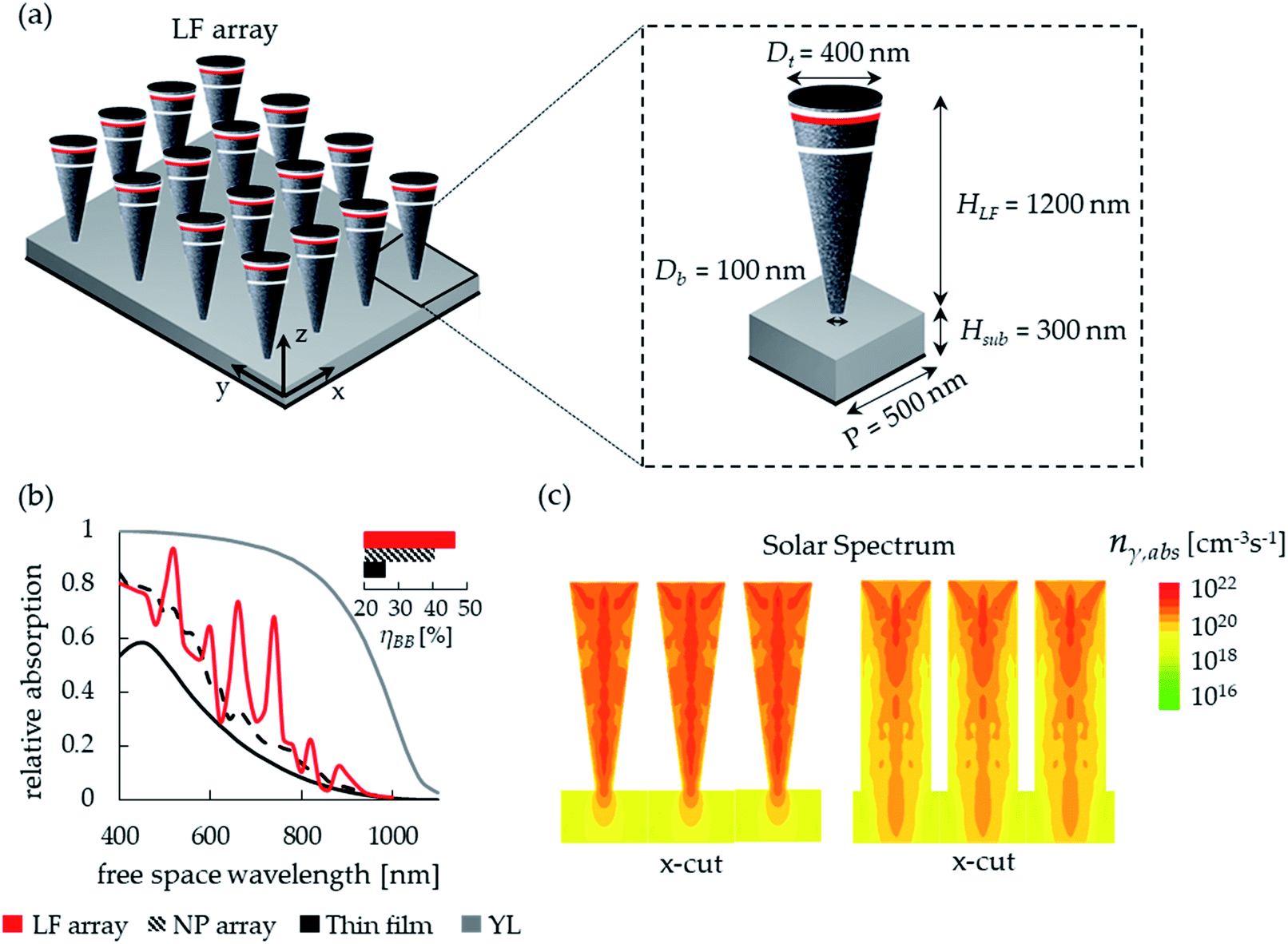
Fig. 1a presents an illustration of a LF array on top of an underlying substrate. The total height of the array–substrate complex is set to 1.5 μm and the period of the both the NP and the LF arrays is set to 500 nm with a top diameter (Dt) of 400 nm to comply with the optically optimized geometry for the absorption of solar radiation.43 The geometry that provides the highest broadband absorption for both the NP array–substrate complex (henceforth, the NP complex) and LF array–substrate complex (henceforth, the LF complex) is for a substrate thickness of 0.3 μm and an array height of 1.2 μm (not shown). Furthermore, the broadband absorption of the LF complex is maximized for a LF bottom diameter (Db) of 100 nm. The selected dimensions are further indicated for a single unit cell in a LF array in Fig. 1a. Also, the electrical configuration is shown where a shallow axial junction (red line) is considered with a 20 nm n-type phosphorus-doped emitter and a p-type boron-doped absorber with a bottom hole contact. The top emitter contact is indicated by a black filled circle and the bottom absorber contact is indicated by a solid black line. The white lines mark the extent of the depletion region. In order to focus on the specific contribution of the LF geometry to carrier collection we do not consider an anti-reflective coating (ARC), a bottom reflector and a back-surface field (BSF). Fig. 1b presents the absorption spectra of the selected LF complex, the NP complex, a thin film of 1.5 μm thickness and the respective Yablonovitch limit (YL). The inset in Fig. 1b presents the broadband absorption efficiency (ηBB) with a 14% enhancement of the LF complex over the optically optimized NP complex. Fig. 1c shows the absorbed photon density (nγ,abs) under illumination of AM 1.5 G solar radiation for both the LF and NP complexes, in which the stronger excitation of the LF complex is evident.
 |
| | Fig. 1 (a) A schematic of a silicon LF array with an axial junction on top of a thin silicon substrate. The schematic of the unit cell provides the geometry considered in the current work. The black circle on top of the LF indicates the top emitter contact and the bottom black rectangle indicates the bottom absorber contact. (b) Relative absorption spectra of the LF complex, the respective NP complex, a 1.5 μm thin film and the Yablonovitch limit. The inset provides the respective broadband absorption efficiencies. (c) Cross-sections of the LF complex and the NP complex presenting nγ,abs under the illumination of the solar spectrum (AM 1.5 G). | |
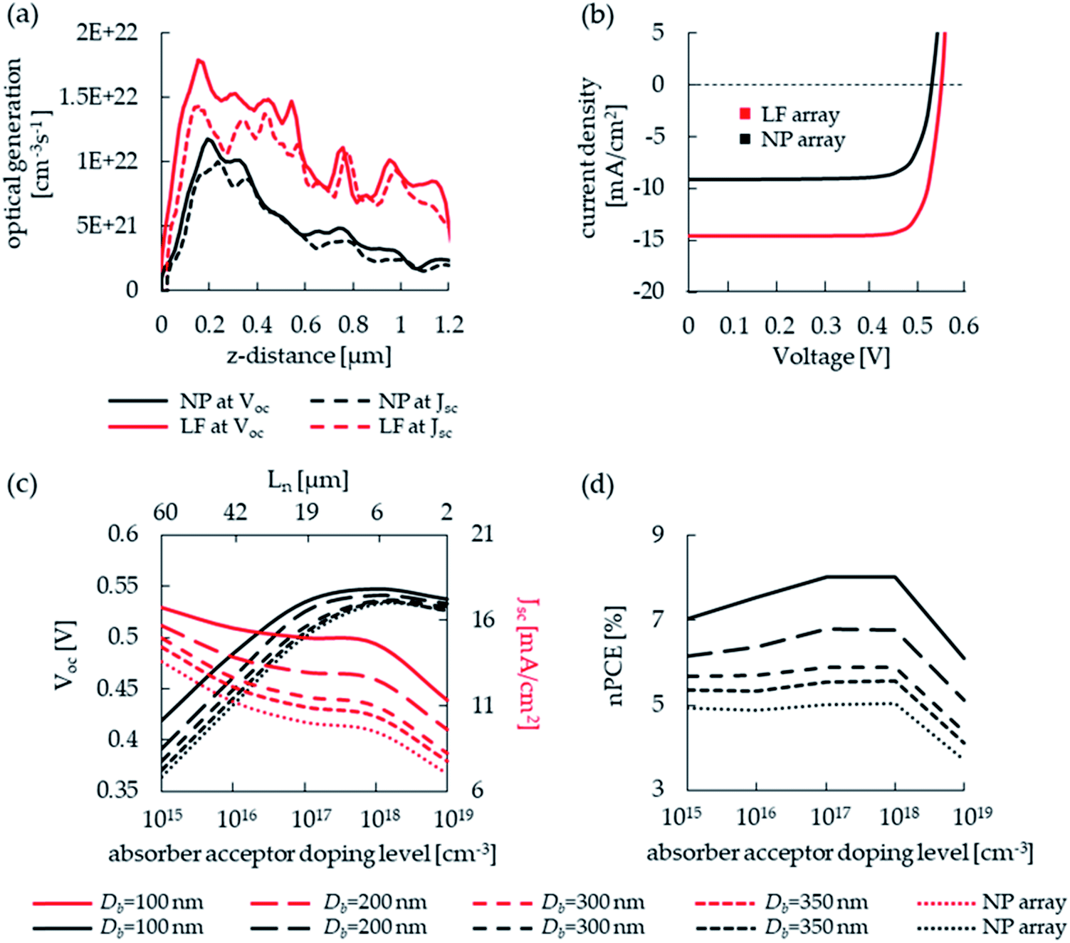
In the following photovoltaic analysis, we construct LF and NP photovoltaic cells from single unit cells in the respective complexes, as presented in the inset in Fig. 1a for the LF cell. Fig. 2a shows the optical generation profiles along the vertical axes of the NP and LF complexes under both Jsc and Voc conditions, where the higher optical generation in the LF complex is evident. Fig. 2b presents current–voltage (I–V) curves for an absorber acceptor doping level (NA) of 1018 cm−3 for both NP and LF photovoltaic cells, where the photocurrent enhancement of the LF cell is a direct consequence of the enhanced optical generation. We next follow the transition from a NP cell into a LF cell by gradually decreasing the NP bottom diameter from Db = 400 nm to Db = 350 nm, 300 nm, 200 nm and 100 nm. The absorption and the optical generation for each geometry were calculated (not shown). Fig. 2c shows the dependency of Jsc and Voc on NA for different Db values. A gradual increase in both Voc and Jsc is noticeable with the decrease in Db for the full range of NA values. Note that Voc reaches a maximum for NA = 1018 cm−3 which is a direct consequence of the saturation current dependency on NA and minority carrier lifetimes which also depend on NA. The respective electron diffusion lengths (Ln) are also presented in Fig. 2c. Fig. 2d presents the dependency of the nominal power conversion efficiency (nPCE), defined as Jsc × Voc/Pin where Pin is the power of the solar spectrum at AM 1.5 G, on NA for all the considered Db values. The nPCE values of all cells peak at NA = 1017 cm−3. The highest nPCE = 8% is obtained for the smallest Db = 100 nm as compared with the NP cell with an nPCE of 5% which reflects an nPCE enhancement of 60%. This is surprising as the ηBB enhancement is only 14%. In order to understand the origin of the 60% nPCE enhancement we next carefully examine the behavior of Jsc and Voc of both LF and NP cells.
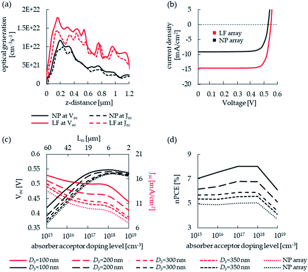 |
| | Fig. 2 (a) Optical generation profiles along the z-axis for the LF and NP cells under Voc and Jsc conditions. Note that z = 0 is the top of the LF. (b) I–V curves of the LF cell and the NP cell for NA = 1018 cm−3 in which the Jsc enhancement in the LF cell is evident. (c) The dependency of Voc and Jsc on NA for different Db values. The top x-axis presents the respective electron minority carrier diffusion lengths. (d) The dependency of nPCE on NA for the different Db values. | |
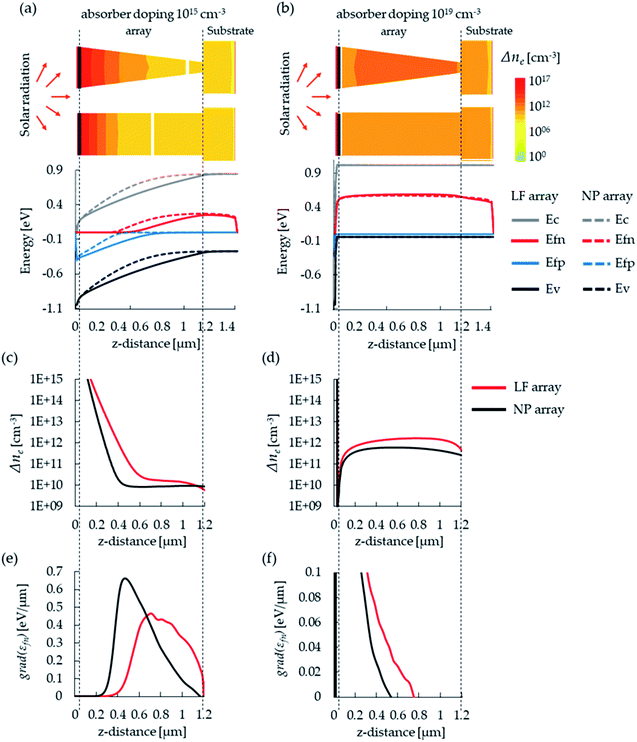
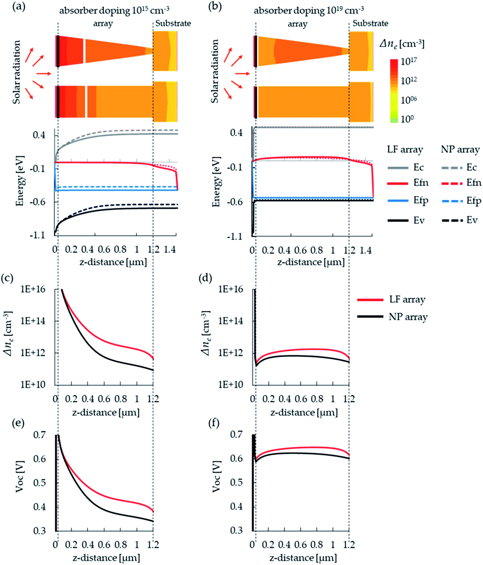
The Voc enhancement of the LF cell over the NP cell decreases with an increase in NA with a highest value of 15% for NA = 1015 cm−3, and with a corresponding Jsc enhancement of 23% (see Fig. 2c). Voc is equal to the splitting of the quasi-Fermi levels (εfc − εfv, where εfc is the electron quasi-Fermi level and εfv is the hole quasi-Fermi level), between the top emitter electron contact and the bottom absorber hole contact, and it is equal to the free energy delivered to the load. Fig. 3a and b present the energy band diagrams along the vertical axes of the LF cell and the NP cell for NA = 1015 cm−3 and 1019 cm−3, respectively. The cross-sections of LF and NP cells above the band diagrams visualize the considered orientation. The Voc values extracted from the energy band diagrams for NA = 1015 cm−3 are 419 mV and 364 mV for the LF and the NP cells, respectively, and similarly for NA = 1019 cm−3 the Voc values are 537 mV and 527 mV. The Voc values extracted from the energy band diagrams are in agreement with the Voc values extracted from the I–V curves (Fig. 2c). Next, we examine the origin of the quasi-fermi level splitting and its dependency on NA. For a p-type absorber (1) Voc = kT![[thin space (1/6-em)]](https://www.rsc.org/images/entities/char_2009.gif) ln(1 + Δne/ne0), where k is the Boltzmann constant, T is the cell temperature (300 K), Δne is the injected photoelectron density and ne0 is the equilibrium electron density.56Fig. 3c and d show the Δne profiles where for NA = 1015 cm−3 the densities are higher than for NA = 1019 cm−3 due to the doping-dependent lifetimes (see methodology). Also, while for NA = 1015 cm−3 Δne of the LF is significantly higher, for NA = 1019 cm−3 Δne values of the LF and NP are similar. Fig. 3e and f present the respective calculated spatially resolved Voc profile for a p-type absorber according to (1). The origin of the higher Voc of the LF cell for NA = 1015 cm−3 is now apparent; the higher broadband absorption and the optical generation of the LF cell entail a higher population of electron minority carriers in the absorber which, for most of the 1D profile, is about one order of magnitude higher than that in the NP cell. This considerably higher excitation of the absorber directly translates into a higher Voc. This difference in absorber excited minority carriers disappears for NA = 1019 cm−3 due to the higher Shockley–Read–Hall (SRH) recombination. However, note that a higher NA presents a higher Voc due to the absorber ne0 which is three orders of magnitude smaller for NA = 1019 cm−3. The enhanced absorber photoelectron density for NA = 1015 cm−3 is also apparent in the 2D cross-section presented in Fig. 3a. Therefore, the higher Voc at NA = 1015 cm−3 in the LF cell is a combination of a higher carrier injection and a lower level of recombination.
ln(1 + Δne/ne0), where k is the Boltzmann constant, T is the cell temperature (300 K), Δne is the injected photoelectron density and ne0 is the equilibrium electron density.56Fig. 3c and d show the Δne profiles where for NA = 1015 cm−3 the densities are higher than for NA = 1019 cm−3 due to the doping-dependent lifetimes (see methodology). Also, while for NA = 1015 cm−3 Δne of the LF is significantly higher, for NA = 1019 cm−3 Δne values of the LF and NP are similar. Fig. 3e and f present the respective calculated spatially resolved Voc profile for a p-type absorber according to (1). The origin of the higher Voc of the LF cell for NA = 1015 cm−3 is now apparent; the higher broadband absorption and the optical generation of the LF cell entail a higher population of electron minority carriers in the absorber which, for most of the 1D profile, is about one order of magnitude higher than that in the NP cell. This considerably higher excitation of the absorber directly translates into a higher Voc. This difference in absorber excited minority carriers disappears for NA = 1019 cm−3 due to the higher Shockley–Read–Hall (SRH) recombination. However, note that a higher NA presents a higher Voc due to the absorber ne0 which is three orders of magnitude smaller for NA = 1019 cm−3. The enhanced absorber photoelectron density for NA = 1015 cm−3 is also apparent in the 2D cross-section presented in Fig. 3a. Therefore, the higher Voc at NA = 1015 cm−3 in the LF cell is a combination of a higher carrier injection and a lower level of recombination.
 |
| | Fig. 3
V
oc conditions: (a) energy band diagrams along the z-axis for LF and NP cells for NA = 1015 cm−3. The cross-sections on top show the respective electron density distribution as well as the location of the metallurgical axial junctions (black line) and depletion lines (white lines). (b) The same as (a) for NA = 1019 cm−3. (c) Δne profiles along the z-axis for NA = 1015 cm−3. (d) The same as (e) for Na = 1019 cm−3. (e) Spatially resolved Voc along the z-axis for NA = 1015 cm−3. (f) The same as (e) for NA = 1019 cm−3. | |
The Jsc enhancement of the LF cell compared with the NP cell increases with NA from 24% to 61% for NA = 1015 cm−3 to 1019 cm−3, respectively (see Fig. 2c). The generation of photocurrent reflects the conversion efficiency of chemical energy into electrical energy. The electron current is described by Je = σe/q grad(εfn), where grad(εfn) is the gradient of the electron quasi-fermi level, q is the elementary charge and σe is the electron conductivity equal to neqμe where ne is the electron density and μe is the electron mobility. Hence a higher σe and grad(εfn) along the electron path towards the emitter contact will induce greater emitter selectivity towards electrons and therefore a higher Je. Fig. 4a and b show the energy band diagrams of the NP and LF cells under Jsc conditions for NA = 1015 cm−3 and 1019 cm−3, respectively, Fig. 4c and d present the respective ne which is linearly proportional to σe, and Fig. 4e and f present the respective grad(εfn) for which it is positive. For NA = 1015 cm−3ne, and hence σe, in the LF cell increases towards the emitter contact more appreciably which provides an enhanced emitter selectivity towards electrons in the LF cell compared with that of the NP cell. grad(εfn) for NA = 1015 cm−3 is positive for both cells, which indicates a decrease in εfn towards the emitter, but it is not necessarily higher in the LF cell as shown in Fig. 4e. Overall for NA = 1015 cm−3 the combined effect of ne and grad(εfn) results in 24% Jsc enhancement. For NA = 1019 cm−3 (Fig. 4f) both σe and grad(εfn) (i.e. where grad(εfn) > 0) are higher in the LF cell. Therefore, the combined enhancement of σe and grad(εfn) results in an overall Jsc enhancement of 61% in the LF cell compared with the NP cell. Importantly, the origin of the higher grad(εfn) in the LF cell is due to the gradient in the electron chemical potential which is due to the higher ne at the LF bottom part which is a direct consequence of the unique LF inverted geometry.
 |
| | Fig. 4
J
sc conditions: (a) energy diagrams along the z-axis for LF and NP cells for NA = 1015 cm−3. The cross-sections on top show the respective electron density distribution as well as the location of the metallurgical axial junctions (black line) and depletion lines (white lines). (b) The same as (a) for NA = 1019 cm−3. (c) Electron density profiles along the z-axis for NA = 1015 cm−3. (d) The same as (c) for NA = 1019 cm−3. (e) grad(εfn) profiles along the z-axis for NA = 1015 cm−3. (f) The same as (e) for NA = 1019 cm−3. | |
3. Conclusions
LF arrays provide efficient broadband absorption of solar radiation that is superior to recent advances in the field. In the current work we show that the unique LF inverted geometry provides additional opportunities for efficient carrier extraction and photovoltaic efficiency enhancement. We show that the relatively high absorption affects the open-circuit voltage on the one hand, and the gradient of the quasi-Fermi level and the minority carrier conductivity in the absorber allow for short-circuit current enhancement, on the other hand. These effects coupled with the right selection of doping levels result in a significant efficiency enhancement. We believe this approach to be important to other absorption-based photonic devices in which carrier extraction is important.
4. Methods
4.1. Finite-difference time-domain electromagnetic calculations
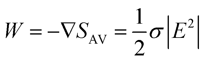
We use 3D finite-difference time-domain (FDTD) electromagnetic calculations with the Advanced TCAD package by Synopsys (Mountain View, CA, USA). The optical excitation is performed with a normally incident plane wave polarized along the x-axis in the spectral range of 400–1100 nm in 20 nm steps. The simulation box size is set to the size of the square unit cell with a periodic boundary condition along the lateral dimensions, and the boundary condition along the vertical axis is set to complementary perfectly matched layers (CPML). The periodic boundary condition is applied to normally incident plane wave excitation using the total-field scattered-field (TFSF) formulation. Both the magnetic and electric fields are copied directly from the periodic facet to the opposing one during field update. The numbers of absorbed photons, reflected photons and transmitted photons are extracted at each wavelength using sensors that are located above and below the unit cell, and the respective relative absorption, reflection and transmission are calculated. The absorbed photon density (nγ,abs) is calculated for each wavelength. nγ,abs is calculated by dividing the absorbed power density ( , where SAV is the time-averaged Poynting vector, σ is the non-zero conductivity and E is the electric field) by the energy of the incident photon. For efficient and accurate FDTD calculations, the maximum mesh cell size is kept smaller than 1/10th of the wavelength in silicon (more than 10 nodes per wavelength). The broadband absorption efficiency (ηBB) is the relative absorption averaged and weighted with the solar spectrum. The considered solar spectrum is Air Mass 1.5 Global (AM 1.5 G). The optical constants of the silicon material are taken from the literature.57
4.2. Electrical device calculations
We use 3D device calculations (Sentaurus, Synopsys Inc.) to examine the optoelectronic and the photovoltaic performance. The Poisson and the Continuity equations are solved at each mesh point for a carrier generation profile, which is calculated from ηBB. The bottom and top contacts define the vertical boundary conditions. The calculated photovoltaic cells are composed of a degenerately phosphorus-doped 5 × 1019 cm−3 emitter (n-type) and a boron-doped absorber (p-type). The carrier generation profile is calculated as follows: for excitation energy greater than or equal to the bandgap energy, the quantum efficiency is set to one, and otherwise, it is set to zero. In every mesh point, the Poisson and the Continuity equations are solved, in which the doping-dependent Shockley–Read–Hall (SRH) recombination, Auger recombination, the bandgap renormalization for degenerately doped silicon and the doping dependent mobility are all accounted for. We consider a standard Czochralski (cz) silicon and the material parameters are set accordingly. The rate of Auger recombination is calculated in the following manner:58| | | RAnet = (Cnn + Cpp) (np − ni,eff2), | (1) |
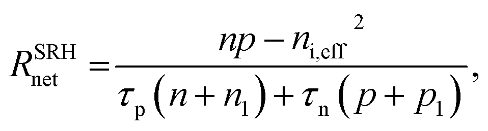
where Cn and Cp were set to 2.9 × 10⁻³¹ cm6 s−1 and 1 × 10⁻³¹ cm6 s−1, respectively.58 The rate of SRH is calculated in the following manner:58| |  | (2) |
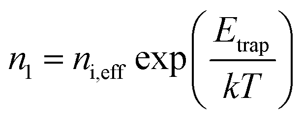
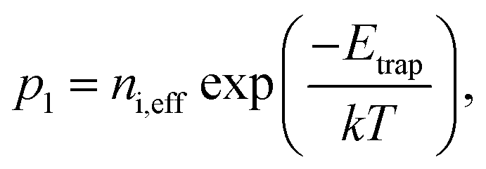
where n and p are the respective electron and hole carrier densities, ni,eff is the effective intrinsic density (accounting for bandgap narrowing), τn and τp are the respective electron and hole lifetimes, and n1 and p1 are:| |  | (3) |
| |  | (4) |
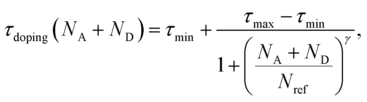
where Etrap, the difference between the defect level and the intrinsic level, is set to zero. The dependency of SRH recombination on doping is reflected in the dependency of carrier lifetime on doping:| |  | (5) |
where NA and ND are the acceptor and donor doping levels, respectively. We select γ = 1, τmin = 0, and Nref = 1016 cm−3 for both holes and electrons, and τmax = 10−6 seconds for electrons and holes, respectively. The considered diffusion coefficient for the electron minority carriers is 36 cm−2 s−1.
Conflicts of interest
The authors declare no conflict of interest.
Acknowledgements
We acknowledge the financial support of this work by the Authority of Innovation, Israel.
References
- M. D. Kelzenberg, D. B. Turner-Evans, M. C. Putnam, S. W. Boettcher, R. M. Briggs, J. Y. Baek, N. S. Lewis and H. A. Atwater, High-Performance Si Microwire Photovoltaics, Energy Environ. Sci., 2011, 4(3), 866–871 RSC.
- P. R. Pudasaini, D. Elam and A. A. Ayon, Aluminum Oxide Passivated Radial Junction Sub-Micrometre Pillar Array Textured Silicon Solar Cells, J. Phys. D: Appl. Phys., 2013, 46(23), 235104 CrossRef.
- H. P. Yoon, Y. a. Yuwen, C. E. Kendrick, G. D. Barber, N. J. Podraza, J. M. Redwing, T. E. Mallouk, C. R. Wronski and T. S. Mayer, Enhanced Conversion Efficiencies for Pillar Array Solar Cells Fabricated from Crystalline Silicon with Short Minority Carrier Diffusion Lengths, Appl. Phys. Lett., 2010, 96(21), 213503 CrossRef.
- E. C. Garnett and P. Yang, Silicon Nanowire Radial P-n Junction Solar Cells, J. Am. Chem. Soc., 2008, 130(29), 9224–9225 CrossRef CAS PubMed.
- E. Garnett and P. Yang, Light Trapping in Silicon Nanowire Solar Cells, Nano Lett., 2010, 10(3), 1082–1087 CrossRef CAS PubMed.
- L. Tsakalakos, J. Balch, J. Fronheiser, B. a. Korevaar, O. Sulima and J. Rand, Silicon Nanowire Solar Cells, Appl. Phys. Lett., 2007, 91(23), 233117 CrossRef.
- H. Li, R. Jia, C. Chen, Z. Xing, W. Ding, Y. Meng, D. Wu, X. Liu and T. Ye, Influence of Nanowires Length on Performance of Crystalline Silicon Solar Cell, Appl. Phys. Lett., 2011, 98(15), 151116 CrossRef.
- T. Stelzner, M. Pietsch, G. Andrä, F. Falk, E. Ose and S. Christiansen, Silicon Nanowire-Based Solar Cells, Nanotechnology, 2008, 19(29), 295203 CrossRef PubMed.
- M. Gharghi, On the Design and Applicability of Nanowire Solar Cells Using Low-Grade Semiconductors, J. Appl. Phys., 2012, 111, 034501 CrossRef.
- M. Gharghi, E. Fathi, B. Kante, S. Sivoththaman and X. Zhang, Heterojunction Silicon Microwire Solar Cells, Nano Lett., 2012, 12(12), 6278–6282 CrossRef CAS PubMed.
- S. W. Schmitt, G. Brönstrup, G. Shalev, S. K. Srivastava, M. Y. Bashouti, G. H. Döhler and S. H. Christiansen, Probing Photo-Carrier Collection Efficiencies of Individual Silicon Nanowire Diodes on a Wafer Substrate, Nanoscale, 2014, 6, 7897–7902 RSC.
- G. Shalev, S. W. Schmitt, E. Heidemarie, G. Brönstrup and S. Christiansen, Enhanced Photovoltaics Inspired by the Fovea Centralis, Sci. Rep., 2015, 5, 8570 CrossRef CAS PubMed.
- H.-P. Wang, K.-Y. Lai, Y.-R. Lin, C.-A. Lin and J.-H. He, Periodic Si Nanopillar Arrays Fabricated by Colloidal Lithography and Catalytic Etching for Broadband and Omnidirectional Elimination of Fresnel Reflection, Langmuir, 2010, 26(15), 12855–12858 CrossRef CAS PubMed.
- W. Wang, S. Wu, K. Reinhardt, Y. Lu and S. Chen, Broadband Light Absorption Enhancement in Thin-Film Silicon Solar Cells, Nano Lett., 2010, 10(6), 2012–2018 CrossRef CAS PubMed.
- G. Jia, M. Steglich, I. Sill and F. Falk, Core–shell Heterojunction Solar Cells on Silicon Nanowire Arrays, Sol. Energy Mater. Sol. Cells, 2012, 96, 226–230 CrossRef CAS.
- G. Jia, A. Gawlik, J. Bergmann, B. Eisenhawer, S. Schonherr, G. Andra and F. Falk, Silicon Nanowire Solar Cells with Radial P-n Heterojunction on Crystalline Silicon Thin Films: Light Trapping Properties, IEEE J. Photovolt., 2014, 4(1), 28–32 Search PubMed.
- O. Gunawan, K. Wang, B. Fallahazad, Y. Zhang, E. Tutuc and S. Guha, High Performance Wire-Array Silicon Solar Cells, Prog. Photovoltaics, 2011, 19, 307–312 CAS.
- J. Li, H. Yu, S. M. Wong, G. Zhang, X. Sun, P. G.-Q. Lo and D.-L. Kwong, Si Nanopillar Array Optimization on Si Thin Films for Solar Energy Harvesting, Appl. Phys. Lett., 2009, 95, 033102 CrossRef.
- S. M. Wong, H. Y. Yu, J. S. Li, G. Zhang, P. Lo and D. L. Kwong, Design High-Efficiency Si Nanopillar-Array-Textured Thin-Film Solar Cell, IEEE Electron Device Lett., 2010, 31(4), 335–337 CAS.
- S. M. Wong, H. Y. Yu, J. S. Li, Y. L. Li, N. Singh, P. G. Q. Lo and D. L. Kwong, Si Nanopillar Array Surface-Textured Thin-Film Solar Cell With Radial p–n Junction, IEEE Electron Device Lett., 2011, 32(2), 176–178 CAS.
- K. Taretto and U. Rau, Modeling Extremely Thin Absorber Solar Cells for Optimized Design, Prog. Photovoltaics, 2004, 12, 573–591 CAS.
- D. M. Callahan, J. N. Munday and H. a. Atwater, Solar Cell Light Trapping beyond the Ray Optic Limit, Nano Lett., 2012, 12(1), 214–218 CrossRef CAS PubMed.
- Z. Yu, A. Raman and S. Fan, Fundamental Limit of Nanophotonic Light Trapping in Solar Cells, Proc. Natl. Acad. Sci. U. S. A., 2010, 107(41), 17491–17496 CrossRef CAS PubMed.
- B. C. P. Sturmberg, K. B. Dossou, L. C. Botten, A. A. Asatryan, C. G. Poulton, C. M. de Sterke and R. C. McPhedran, Modal Analysis of Enhanced Absorption in Silicon Nanowire Arrays, Opt. Express, 2011, 19(S5), A1067 CrossRef CAS PubMed.
- K. T. Fountaine, W.-H. Cheng, C. R. Bukowsky and H. a. Atwater, Near-Unity Unselective Absorption in Sparse InP Nanowire Arrays, ACS Photonics, 2016, 3(10), 1826–1832 CrossRef CAS.
- L. Hu and G. Chen, Analysis of Optical Absorption in Silicon Nanowire Arrays for Photovoltaic Applications, Nano Lett., 2007, 7(11), 3249–3252 CrossRef CAS PubMed.
- Y.-F. Huang, S. Chattopadhyay, Y.-J. Jen, C.-Y. Peng, T.-A. Liu, Y.-K. Hsu, C.-L. Pan, H.-C. Lo, C.-H. Hsu and Y.-H. Chang,
et al., Improved Broadband and Quasi-Omnidirectional Anti-Reflection Properties with Biomimetic Silicon Nanostructures, Nat. Nanotechnol., 2007, 2(12), 770–774 CrossRef CAS PubMed.
- S. Jeong, M. D. McGehee and Y. Cui, All-Back-Contact Ultra-Thin Silicon Nanocone Solar Cells with 13.7% Power Conversion Efficiency, Nat. Commun., 2013, 4, 2950 CrossRef PubMed.
- H. Savin, P. Repo, G. von Gastrow, P. Ortega, E. Calle, M. Garín and R. Alcubilla, Black Silicon Solar Cells with Interdigitated Back-Contacts Achieve 22.1% Efficiency, Nat. Nanotechnol., 2015, 10, 1–6 CrossRef PubMed.
- M. L. Brongersma, Y. Cui and S. Fan, Light Management for Photovoltaics Using High-Index Nanostructures, Nat. Mater., 2014, 13(5), 451–460 CrossRef CAS PubMed.
- E. R. Martins, J. Li, Y. Liu, V. Depauw, Z. Chen, J. Zhou and T. F. Krauss, Deterministic Quasi-Random Nanostructures for Photon Control, Nat. Commun., 2013, 4, 2665 CrossRef PubMed.
- M.-C. van Lare and A. Polman, Optimized Scattering Power Spectral Density of Photovoltaic Light-Trapping Patterns, ACS Photonics, 2015, 2(7), 822–831 CrossRef CAS.
- A. Gaucher, A. Cattoni, C. Dupuis, W. Chen, R. Cariou, M. Foldyna, L. Lalouat, E. Drouard, C. Seassal, I. Roca and P. Cabarrocas,
et al., Ultrathin Epitaxial
Silicon Solar Cells with Inverted Nanopyramid Arrays for Efficient Light Trapping, Nano Lett., 2016, 16(9), 5358–5364 CrossRef CAS PubMed.
- M. Y. Bashouti, P. Yousefi, J. Ristein and S. H. Christiansen, Electronic Properties of Si–Hx Vibrational Modes at Si Waveguide Interface, J. Phys. Chem. Lett., 2015, 6(19), 3988–3993 CrossRef CAS PubMed.
- G. Shalev, Addressing Carrier Extraction from Optically Optimized Nanopillar Arrays for Thin-Film Photovoltaics, Nanoscale, 2017, 9, 15707–15716 RSC.
- P. Spinelli, M. A. Verschuuren and A. Polman, Broadband Omnidirectional Antireflection Coating Based on Subwavelength Surface Mie Resonators, Nat. Commun., 2012, 3, 692 CrossRef CAS PubMed.
- S. K. Kim, X. Zhang, D. J. Hill, K. D. Song, J. S. Park, H. G. Park and J. F. Cahoon, Doubling Absorption in Nanowire Solar Cells with Dielectric Shell Optical Antennas, Nano Lett., 2015, 15(1), 753–758 CrossRef CAS PubMed.
- Y. Li, M. Li, P. Fu, R. Li, D. Song, C. Shen and Y. Zhao, A Comparison of Light-Harvesting Performance of Silicon Nanocones and Nanowires for Radial-Junction Solar Cells, Sci. Rep., 2015, 5, 11532 CrossRef CAS PubMed.
- A. B. Wong, S. Brittman, Y. Yu, N. P. Dasgupta and P. Yang, Core-Shell CdS-Cu2S Nanorod Array Solar Cells, Nano Lett., 2015, 15(6), 4096–4101 CrossRef CAS PubMed.
- A. Nowzari, M. Heurlin, V. Jain, K. Storm, A. Hosseinnia, N. Anttu, M. T. Borgström, H. Pettersson and L. Samuelson, A Comparative Study of Absorption in Vertically and Laterally Oriented InP Core-Shell Nanowire Photovoltaic Devices, Nano Lett., 2015, 15(3), 1809–1814 CrossRef CAS PubMed.
- J. Wallentin, N. Anttu, D. Asoli, M. Huffman, I. Aberg, M. H. Magnusson, G. Siefer, P. Fuss-Kailuweit, F. Dimroth and B. Witzigmann,
et al., InP Nanowire Array Solar Cells Achieving 13.8% Efficiency by Exceeding the Ray Optics Limit, Science, 2013, 339(6123), 1057–1060 CrossRef CAS PubMed.
- G. Vescovi, D. Asoli, U. Naseem, J. P. Gilboy, C. Sundvall, A. Dahlgren, K. E. Svensson, N. Anttu, M. T. Bj and L. Samuelson, A GaAs Nanowire Array Solar Cell with 15.3 % Efficiency at 1 Sun, IEEE J. Photovolt., 2016, 6(1), 185–190 Search PubMed.
- G. Shalev, S. Schmitt, G. Brönstrup and S. Christiansen, Maximizing the Ultimate Absorption Efficiency of Vertically-Aligned Semiconductor Nanowire Arrays with Wires of a Low Absorption Cross-Section, Nano Energy, 2015, 12, 801–809 CrossRef CAS.
- R. R. Lapierre, Numerical Model of Current-Voltage Characteristics and Efficiency of GaAs Nanowire Solar Cells, J. Appl. Phys., 2011, 109, 034311 CrossRef.
- P. Krogstrup, H. I. Jørgensen, M. Heiss, O. Demichel, J. V. Holm, M. Aagesen, J. Nygard and A. Fontcuberta i Morral, Single-Nanowire Solar Cells beyond the Shockley–Queisser Limit, Nat. Photonics, 2013, 7(4), 306–310 CrossRef CAS.
- J. Oh, H.-C. Yuan and H. M. Branz, An 18.2%-Efficient Black-Silicon Solar Cell Achieved through Control of Carrier Recombination in Nanostructures, Nat. Nanotechnol., 2012, 7(11), 743–748 CrossRef CAS PubMed.
- B. M. Kayes, H. A. Atwater and N. S. Lewis, Comparison of the Device Physics Principles of Planar and Radial P-n Junction Nanorod Solar Cells, J. Appl. Phys., 2005, 97, 114302 CrossRef.
- J. D. Christesen, X. Zhang, C. W. Pinion, T. a Celano, C. J. Flynn and J. F. Cahoon, Design Principles for Photovoltaic Devices Based on Si Nanowires with Axial or Radial P-n Junctions, Nano Lett., 2012, 12(11), 6024–6029 CrossRef CAS PubMed.
- F. Wang, H. Yu, J. Li, S. Wong, X. W. Sun, X. Wang and H. Zheng, Design Guideline of High Efficiency Crystalline Si Thin Film Solar Cell with Nanohole Array Textured Surface, J. Appl. Phys., 2011, 109(8), 084306-1–084306-5 Search PubMed.
- H. Li, D. Lee and W. J. Yoo, Optoelectronic Performance of Radial-Junction Si Nanopillar and Nanohole Solar Cells, IEEE Trans. Electron Devices, 2012, 59(9), 2368–2374 CAS.
- S. S. P. Konedana, E. Vaida, V. Viller and G. Shalev, Optical Absorption beyond the Yablonovitch Limit with Light Funnel Arrays, Nano Energy, 2019, 59, 321–326 CrossRef CAS.
- A. Prajapati, A. Chauhan, D. Keizman and G. Shalev, Approaching the Yablonovitch Limit with Free-Floating Arrays of Subwavelength Trumpet Non-Imaging Light Concentrators Driven by Extraordinary Low Transmission, Nanoscale, 2019, 11, 3681–3688 RSC.
- A. Prajapati, Y. Nissan, T. Gabay and G. Shalev, Light Trapping with Silicon Light Funnel Arrays, Materials, 2018, 11(3), 1–9 CrossRef PubMed.
- A. Prajapati, Y. Nissan, T. Gabay and G. Shalev, Broadband Absorption of the Solar Radiation with Surface Arrays of Subwavelength Light Funnels, Nano Energy, 2018, 54, 447–452 CrossRef CAS.
- G. Marko, A. Prajapati and G. Shalev, Broadband Absorption of the Solar Radiation with Arrays of Subwavelength Nonimaging Light Concentrators, Nano Energy, 2019, 61, 275–283 CrossRef CAS.
-
P. Wurfel and U. Wurfel, Physics of Solar Cells - From Principles to New Concepts, Wiley-VCH, Weinheim, 2016 Search PubMed.
-
E. D. Palik, Handbook of Optical Constants of Solids, Academic, 1985 Search PubMed.
- W. Lochmann and A. Haugt, Phonon-Assisted Auger Recombination in Si with Direct Calculation of the Overlap Integrals, Solid State Commun., 1980, 35(5), 553–556 CrossRef CAS.
|
| This journal is © The Royal Society of Chemistry 2019 |
Click here to see how this site uses Cookies. View our privacy policy here. 
 Open Access Article
 This Open Access Article is licensed under a Creative Commons Attribution-Non Commercial 3.0 Unported Licence
 a and
G.
Shalev
a and
G.
Shalev

 , where SAV is the time-averaged Poynting vector, σ is the non-zero conductivity and E is the electric field) by the energy of the incident photon. For efficient and accurate FDTD calculations, the maximum mesh cell size is kept smaller than 1/10th of the wavelength in silicon (more than 10 nodes per wavelength). The broadband absorption efficiency (ηBB) is the relative absorption averaged and weighted with the solar spectrum. The considered solar spectrum is Air Mass 1.5 Global (AM 1.5 G). The optical constants of the silicon material are taken from the literature.57