
 Open Access Article
 This Open Access Article is licensed under a Creative Commons Attribution-Non Commercial 3.0 Unported Licence
An efficient flexible graphene-based light-emitting device†
Guangya
Jiang‡
 abc,
He
Tian‡
*ab,
Xue-Feng
Wang
ab,
Thomas
Hirtz
ab,
Fan
Wu
ab,
Yan-Cong
Qiao
ab,
Guang-Yang
Gou
ab,
Yu-Hong
Wei
ab,
Jing-Ming
Yang
ab,
Sifan
Yang
c,
Yi
Yang
*ab and
Tian-Ling
Ren
*ab
abc,
He
Tian‡
*ab,
Xue-Feng
Wang
ab,
Thomas
Hirtz
ab,
Fan
Wu
ab,
Yan-Cong
Qiao
ab,
Guang-Yang
Gou
ab,
Yu-Hong
Wei
ab,
Jing-Ming
Yang
ab,
Sifan
Yang
c,
Yi
Yang
*ab and
Tian-Ling
Ren
*ab
aInstitute of Microelectronics, Tsinghua University, Beijing 100084, China. E-mail: RenTL@tsinghua.edu.cn; yiyang@tsinghua.edu.cn; tianhe88@tsinghua.edu.cn
bBeijing National Research Center for Information Science and Technology (BNRist), Tsinghua University, Beijing 100084, China
cGraduate School at Shenzhen, Tsinghua University, Shenzhen 518055, China
First published on 4th October 2019
Abstract
In recent years, flexible light-emitting devices (LEDs) have become the main focus in the field of display technology. Graphene, a two-dimensional layered material, has attracted great interest in LEDs due to its excellent properties. However, there are many problems such as efficiency, lifetime, and flexibility not well solved. Herein, we have successfully prepared a flexible LED using laser-induced reduced graphene oxide (LIRGO). The LIRGO LED achieves a luminescence lifetime of over 60 hours and a wall plug efficiency of up to 1.4% in a vacuum environment of 0.02 Pa. There are many small luminescent spots randomly distributed on 3.5 × 5 mm2 of LIRGO. LIRGO's luminous behavior can be controlled by modifying the supply voltage and laser reduction intensity. We also explore LIRGO's applications by testing it in different packages and customizable bulbs. Furthermore, as an interesting demo, the LIRGO device can be used to mimic constellations with visual shapes. This work demonstrates LIRGO's great potential in many fields, such as flexible and miniature light sources and displays.
Introduction
The rapid development of flexible electronic products has revolutionized the traditional electronics industry.1–4As an important part of flexible electronic systems, flexible electroluminescent devices are currently the main focus in the field of flexible displays.5–8Since Destriau discovered intrinsic electroluminescence (EL) in 1947, materials and mechanisms of EL have attracted great attention.9 EL refers to the phenomenon of light emission by combining holes from the anode and electrons from the cathode. Solid-state light-emitting devices (LEDs) are generally classified into inorganic LEDs and organic LEDs (OLEDs). Conventional inorganic LEDs are generally composed of hard, powdery or brittle materials, such as glass, lenses, phosphors, and silicones, which are not suitable for flexible applications.10–12 In recent years, the flexible panel of OLEDs has been developed and manufactured.6 Nevertheless, this technology still possesses some drawbacks. For example, ITO, its transparent electrode, is too stiff and fragile to make a flexible device.13 Furthermore, high temperature is required to fabricate the panel, which is generally incompatible with its flexible substrate, such as polyethylene terephthalate (PET).14
As two-dimensional materials, graphene and its derivatives have excellent physical and chemical properties; moreover, they can play an important role in photonic devices.15–17 Graphene-based photoluminescence (PL) has become quite prominent.18–21 However, EL is more attractive than PL because it can illuminate without the need for an additional light source.22 To decrease panel complexity, EL is generally preferred for display applications.
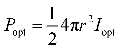
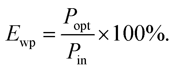
Luminous efficiency is an important indicator of EL. As one of the efficiencies, wall plug efficiency (WPE, Ewp) is the ratio of the radiated optical power (Popt) to the total electric power (Pin) consumed, which is widely used in the field of LEDs.23,24 The formula used is demonstrated as below:
There are many research studies on EL of graphene-based devices.25–30 However, to the best of our knowledge, a graphene-based illuminator with a WPE higher than 1% has not yet been reported. In 2010, M. Freitag et al. observed the thermal infrared emission of biased graphene with a WPE lower than 0.0001%.31 In 2014, R. Beams et al. found EL of graphene excited by electron tunnelling with a WPE lower than 0.0001% too.32 Also in 2014, L. Lawton et al. reported that the WPE of the mid-infrared emission in graphene could reach 0.001%.33 In 2015, Y. Kim et al. discovered the EL of suspended graphene with a WPE of around 0.445%.34 Also in 2015, X. Wang et al. designed a spectrally tunable graphene-based field-effect LED with a WPE less than 0.7%.35 In 2018, Michael C. Chong et al. found bright EL from single graphene nanoribbon junctions, which has a WPE lower than 0.01%.29 Moreover, previously reported graphene-based LEDs had deficient lifetime and seemed to lack concrete applications.
Graphene oxide (GO) is a good candidate for luminescent materials. The electrical properties of GO are directly related to the proportion of different functional groups, which can be controlled by chemical and optical methods.36 Its bandgap can be tuned from 3.5 eV to 1 eV, which corresponds to the wavelength ranging from 350 nm to 1240 nm.37
In this contribution, a light emitter based on laser-induced reduced graphene oxide (LIRGO) is proposed. LIRGO is remarkably flexible and can emit light for more than 60 hours in a 0.02 Pa vacuum. Its WPE is calculated to be 1.4%, which is substantially higher than that of graphene-based light sources reported previously. Moreover, LIRGO possesses micron-scale luminous points and tunable colours that can be used in integrated photonic devices. In addition, LIRGO can be easily patterned at the micrometre scale and has promising applications such as 3D displays and high-resolution displays.
Results and discussion
Device fabrication and luminescence test
A flexible LED based on LIRGO is designed. Fig. 1A illustrates the schematic diagram of the LIRGO device. The details of the fabrication process are shown in Fig. S1.† First, a PET substrate (or other substrates, like polyimide, heat-resistant paper, etc.) is spread on a flat platform. Then, the substrate is coated with a GO solution diluted with tetrahydrofuran. The GO film is formed by air-drying the solution. Thereafter, the surface of the GO film is scanned using a 448 nm laser. As shown in Fig. S1D,† during this step of the process, the yellow GO film turned into black LIRGO. Next, silver electrodes and wires are respectively deposited and soldered on both sides of the LIRGO. Finally, the device is removed from the platform. | ||
| Fig. 1 LIRGO device and its luminescence. (A) Schematic diagram of the LIRGO device. LIRGO is on a flexible substrate. Silver electrodes and wires are placed on both ends. (B) Schematic diagram of LIRGO illumination. When a suitable bias voltage (V) is applied, luminescent spots appear on the LIRGO. (C) The photo of real luminous LIRGO and (D) the zoomed-in image.There are many luminous points with colour differences. (E) LIGRO pattern obtained by laser reduction from GO. LIGRO film also shows good flexibility. (F) The emission spectrum of LIRGO. The spectrum can be divided into three peaks. The inset shows a photomicrograph of a light-emitting region. | ||
By placing the LIRGO device inside vacuum and applying a voltage, steady and bright visible light can be observed (Fig. 1B and C). Fig. 1D shows the details that biased LIRGO contains multiple lighting points with different nuances of colour. More photos of the luminous points with colour differences on LIRGO can be found in Fig. S2.†
We proceed to characterize the stability and lifetime of the LIRGO emitter by carrying out a continuous 60 hour illumination in a vacuum of 0.02 Pa. This experiment was highly valuable since previous studies related to the lifetime of graphene-based LEDs have been scarce. Indeed, many reports have glossed over this issue or had unsatisfactory results.
By measuring the luminous intensity and power consumption of LIRGO, its WPE can be obtained. For the five devices measured at the compliance current set at 0.01 A, the WPEs ranged from 1.2% to 1.7% with an average of 1.4%. See the Experimental section for the calculation details.
As shown in Fig. 1E, the programmable laser equipment can directly generate LIRGO patterns on the GO film with a resolution down to 10 μm. More LIRGO patterns can be found in Fig. S3.† Moreover, LIRGO devices fabricated on materials have good flexibility and can be bent over 90°. In addition, the residual of the GO film can be removed by water immersion, leaving the LIRGO pattern.
The luminescence spectrum of LIRGO exhibits a broad wavelength range, as shown in Fig. 1F. The spectrum of LIRGO is quite different from that of previously reported graphene devices. Prior studies mainly produced devices emitting infrared light and were based on the black body radiation model.31 The luminescence spectrum in Fig. 1F can be divided into three peaks at 850, 910, and 1020 nm, respectively, which can be explained by the specific structure and defects produced by the laser reduction in LIRGO.
Characterization and analysis
Fig. 2A shows the black LIRGO surrounded by the yellow GO film. To observe the differences between LIRGO and GO, the regions of their boundary are shown in the optical micrograph of Fig. 2B. Fig. 2B also highlights the irregularity of the LIRGO surface. Fig. 2C illustrates a schematic diagram of the cross section of LIRGO and indicates that LIRGO is constituted of several layers. Fig. 2D shows an SEM image showing the cross section of the GO-LIRGO junction. Note that there are lots of fluffy layers inside LIRGO. According to a previous study of X. Wang et al., there are semi-reduced GO (semi-rGO) layers in LIRGO.35 Fig. S4B† shows an exposed inside layer when the upper reduced GO (rGO) is removed. This layer has a unique lustre and looks different from GO and rGO, which verifies the presence of semi-rGO layers.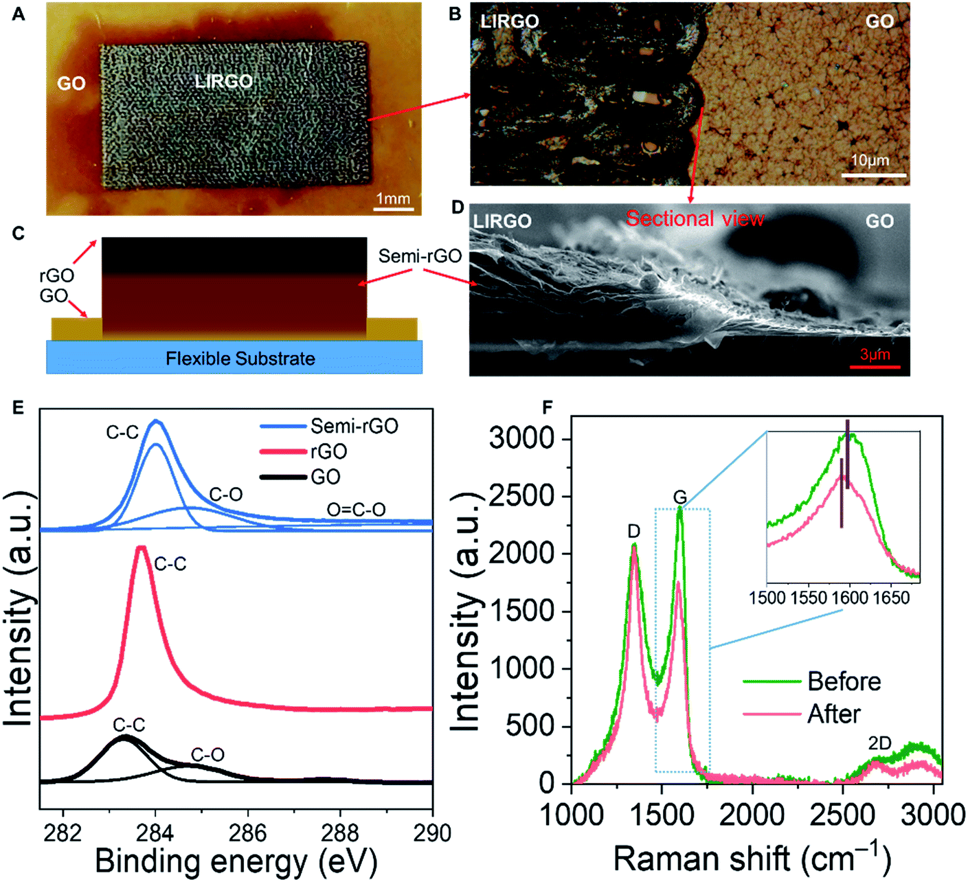 | ||
| Fig. 2 The characterization of LIRGO. (A) Top view of real LIRGO. The yellow area is the GO film while the black one is LIRGO. (B) Optical micrograph of the boundary between LIRGO and GO. (C) Schematic diagram of the cross section of LIRGO. RGO, semi-rGO, GO, and the flexible substrate are distributed from top to bottom. (D) SEM of the cross section of LIRGO and GO. There are semi-rGO layers in the multilayer structure of LIRGO. (E) The XPS spectra of the covalent bonds of C among GO, rGO, and semi-rGO. (F) The Raman spectra of LIRGO before and after light emission. The inset shows the slight difference in the G peak. | ||
To evaluate the changes from GO to LIRGO, conductivity, XPS, and TEM characterization experiments were performed. The sheet resistance of GO is as high as 10 mega ohms, but that of LIRGO is as low as 500 ohms, which indicates that LIRGO's electronic transmission capability is better than GO's. Fig. 2E shows the XPS spectra and the carbon peaks of GO, rGO, and semi-rGO. RGO contains only C–C bonds due to sufficient reduction. GO contains C–C and C–O bonds. Due to partial reduction, semi-rGO contains O![[double bond, length as m-dash]](https://www.rsc.org/images/entities/char_e001.gif) C–O bonds in addition to C–C and C–O bonds. The TEM images indicate the changes of crystal lattices from GO to LIRGO (Fig. S5†). Fig. S5B† shows that there is no periodic lattice in GO, indicating that many oxygen functional groups and defects exist in GO. However, hexagonal honeycomb lattices in LIRGO (Fig. S5D and F†) indicate that LIRGO is partially crystallized. It is notable that the crystals are not destroyed during the luminescence.
C–O bonds in addition to C–C and C–O bonds. The TEM images indicate the changes of crystal lattices from GO to LIRGO (Fig. S5†). Fig. S5B† shows that there is no periodic lattice in GO, indicating that many oxygen functional groups and defects exist in GO. However, hexagonal honeycomb lattices in LIRGO (Fig. S5D and F†) indicate that LIRGO is partially crystallized. It is notable that the crystals are not destroyed during the luminescence.
The Raman spectra of LIRGO before and after luminescence (Fig. 2F) reveal the changes during the light-emitting process. The D peak, the G peak, and the 2D peak of LIRGO can be clearly observed. From the ratio of the 2D peak to the G peak, the multi-layer stack of graphene films can be confirmed. The G peak is stronger than the D peak before illumination. However, after illumination, the G peak is a little weaker than the D peak, which indicates the oxidation of LIRGO and therefore the presence of remaining oxygen in a 0.02 Pa vacuum environment. This oxidation produces more defects and weakens the sp2 C–C bond. Moreover, the G peak has a small shift to left after the luminescence, which indicates a slight reduction of the LIRGO doping level. This is probably due to the dehydration caused by the heat of the luminescence.38 Apart from this, there are no more obvious changes.
In addition, there is no significant change in the conductivity of LIRGO during the emission of bright light, which is similar to the result of Y. Kim et al.34 Therefore, LIRGO is not damaged during the luminescence induced by a moderate electric field, which can explain the durability and reproducibility in LIRGO's illumination.
EL mechanism and model
EL can be generally divided into two types. The first is P–N junction EL and the second is high field EL.39–43 The P–N junction has an electrical polarity. We conducted a polarity experiment to test if the LIRGO's emission is related to the P–N junction EL. Fig. S6A† shows the measurement setup with four pads. The actual image is shown in Fig. S6B.† A bias is applied between pad 1 and pad 3, or pad 2 and pad 4. A luminescence image is captured when the current just exceeds the threshold current. As shown in Fig. S6C and D,† there is no difference in illumination when the polarity of the bias is changed, which confirms a non-polar photon emission and excludes the p–n junction EL. So light emission from LIRGO is basically based on high field EL.However, the mechanism of LIRGO's luminescence differs from that of previous graphene's luminescence based purely on thermal electrons.44 The surface temperature of LIRGO during luminescence is much lower than the temperature required for light emission induced by pure hot electrons (see Fig. S7†).
Therefore, the electric field-assisted thermal ionization, also known as Poole–Frenkel emission, can be the possible mechanism for light emission from LIRGO.35 Under an electric field, the holes obtain sufficient kinetic energy and collide with the defects to generate electrons. The electrons generated after the collision acquire a certain kinetic energy. Electrons with high energy can jump into the conduction band, while electrons with low energy are captured by traps in the forbidden band. The excited electrons formed by the collision are unstable. When the excited electrons recombine with the holes, the energy will be released in the form of photons (Fig. 3A).9,45
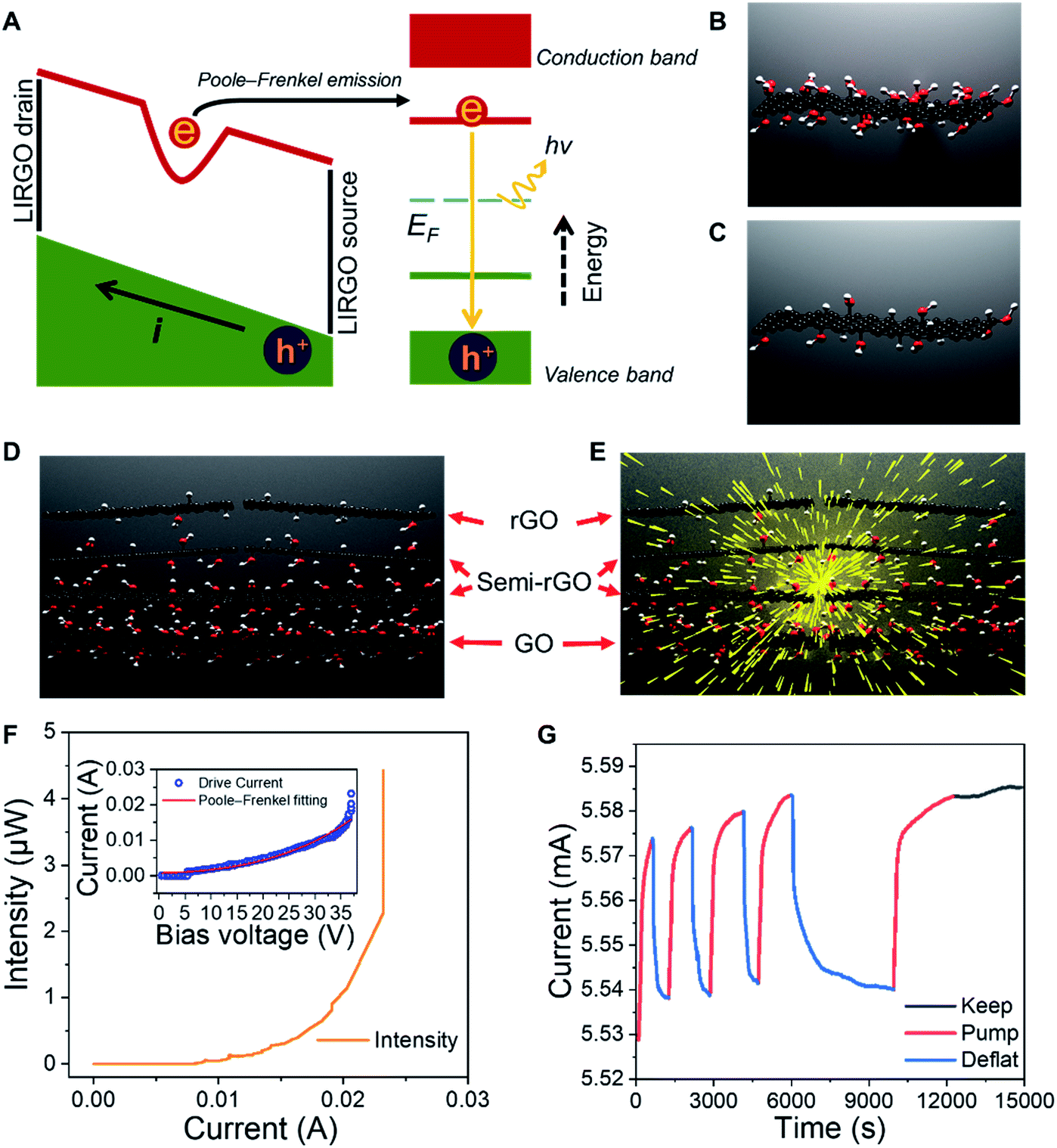 | ||
| Fig. 3 Mechanism analysis and test. (A) Schematic diagram of the EL process of LIRGO. The trapped electrons are excited to the lowest unoccupied discrete energy level by Poole–Frenkel emission. And the excited electron recombines with the hole in the valence band, resulting in photon emission. (B) Schematic diagram of the GO flake. (C) Schematic diagram of the semi-rGO flake. (D) Schematic diagram of the microstructure of LIRGO. (E) Schematic diagram of the luminescence of LIRGO. (F) The light intensity vs. driving current in a vacuum. The inset shows the I–V curve and its Poole–Frenkel fitting curve. (G) The current vs. the pumping, venting or holding conditions at a fixed bias. | ||
The semi-rGO can be the possible light-emitting material in LIRGO. GO flakes are stacked at different depths in the GO film (Fig. S8B†), which can also be inferred from the cross-sectional SEM images in Fig. 2D and S9.† A GO flake inside the GO film (Fig. 3B) is a monoatomic sheet with lateral dimension ranging from 500 nm to 10 μm. After being reduced using a laser, its oxygen-containing functional groups are decreased, as shown in Fig. 3C. The deeper the flakes in LIRGO, the more the functional groups retain after laser induced reduction (Fig. 3D). Therefore, the rGO layers, the semi-rGO layers, and the unreduced GO layers are stacked from top to bottom in LIRGO (Fig. S8C†). The zero-bandgap nature of upper rGO results in a large non-radiative decay rate of stimulated electron–hole pairs, while the bandgap of GO is extremely large.37 The bandgaps of semi-rGO can range from 1.6 to 3.2 eV, which corresponds to the visible range.35 Therefore, semi-rGO flakes emit visible light, as shown in Fig. 3E.
Since the semi-rGO flakes are quite small, their bandgaps are not all direct bandgaps due to the edge effect.46 Therefore, the recombination of electrons and holes generates heat as well. Moreover, there is a sudden decrease in thermal conductivity at high current densities and high temperatures in graphene.34,47 These properties promote spatial accumulation of hot electrons and therefore emission of light in a single semi-rGO flake.
The bandgap of each semi-rGO flake is different, so the emitted photons have different wavelengths and colours, which is consistent with the colour differences in Fig. 1D and the multiple peaks in Fig. 1F.
If the bias voltage increases, more electrons are excited to high energy levels due to collisions or thermal excitation. Consequently, if the voltage is too large, many hot electrons will be produced, which can cause an avalanche effect and damage the device.
Model validation
We measured the luminescence properties of the device in a vacuum. Fig. 3F shows the relationship between light intensity and driving current. Almost no light is emitted when the drive current is below 0.01 A. After the current exceeds 0.02 A, the light intensity sharply increases. In addition, the inset of Fig. 3F shows that the I–V curve can be well fitted by the Poole–Frenkel curve. This indicates that the photon emission of LIRGO conforms to the Poole–Frenkel effect.35We also notice the doping and de-doping effects during pumping and venting, as shown in Fig. 3G. At constant bias, the current increases during the pumping and decreases during the venting. The current passing through the device is steady when the air pressure is held. Due to the water molecules in the air, when the chamber vents, some doping effects take place in LIRGO and increase the energy required for the electronic excitation.38 Therefore, the current in the air is lower, and the light is weaker and easier to quench in air.
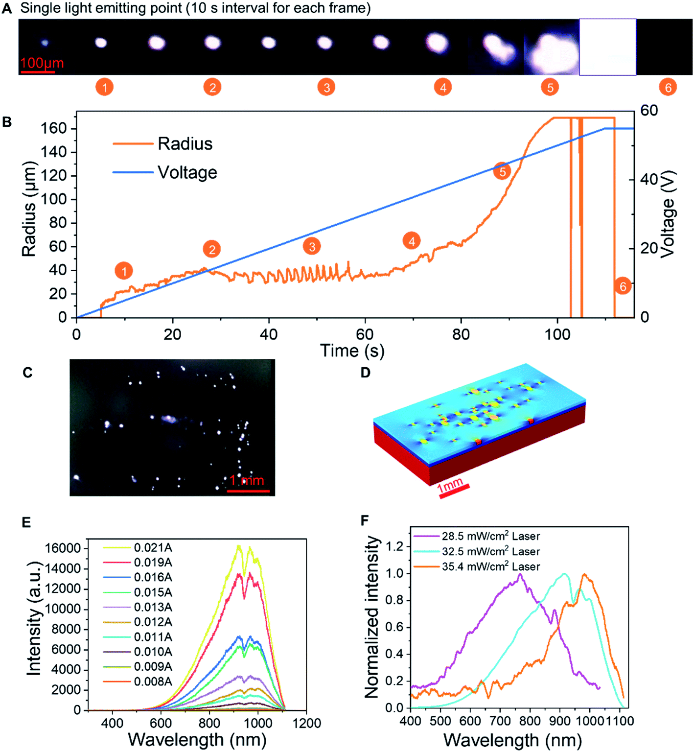
Fig. 4A and B record the changes in the lateral dimension of a single luminescent spot. The light spot is very small, approximately 10 μm, which fits well with our theory of single semi-rGO flake's luminescence. In the beginning, when the voltage is very low, the luminescence is very weak. As the voltage increases, the size of the spot remains stable and does not expand markedly, which strengthens the single semi-rGO flake illumination theory. When the voltage becomes larger, the lateral dimension will rise rapidly because of the increase and combination of the light-emitting points. At very high bias, the device will break down after an intense illumination. The video of the whole process can be found in Movie S1.†
 | ||
| Fig. 4 Single point testing, COMSOL analysis, and spectral changes demonstrating the EL mechanism. (A) The single light-emitting point vs. time at an increasing driving voltage. (B) The lateral dimension (radius) and driving voltage vs. time. (C) Lighting LIRGO with randomly distributed luminous points. (D) Simulation results of randomly distributed light points with COMSOL. (E) The luminescence spectra at different drive currents from a single LIRGO made using a 32.5 mW cm−2 laser. (F) Normalized spectra for LIRGOs made using different laser powers. The current used for LIRGO made using a laser power of 28.5 mW cm−2, 32.5 mW cm−2 and 35.4 mW cm−2 is 0.023 A, 0.019 A and 0.031 A, respectively. | ||
After applying an appropriate bias, many light-emitting points appear on the surface of the LIRGO, as shown in Fig. 4C. EL requires superheated electrons, in which high electric field density and sufficient source electrons are needed. Only areas with a lower resistance will be more likely to obtain a higher current density and therefore emit light. In LIRGO, semi-rGO flakes have different degrees of reduction and are randomly stacked and contacted. Different areas have different resistances. Consequently, when LIRGO starts to emit light, the positions of lighting points are random.
We simulated the model of randomly distributed semi-rGO flakes using Comsol Multiphysics, as shown in Fig. 4D. Due to the different overlapping areas among the semi-rGO flakes, some regions with larger overlapping areas may have lower electrical resistance. Therefore, they have a larger local current density at a bias voltage. The semi-rGO flakes in these areas are more likely to light first.
The wavelength of the luminescence is affected by the crystal structure and the doping level in the semi-rGO flakes. Fig. 4E shows the change in the spectrum in relation to the current. The spectrum of a device is formed by many luminous spots on the LIRGO surface. However, all spectral components are amplified with the increasing voltage. Therefore, the total spectrum has statistical significance. While processing LIRGO samples, we changed the laser reduction intensity and discovered that the spectral centroid is related to the laser intensity (Fig. 4F). Different laser intensities can change the degree of reduction of the GO flakes as a whole. The lower the degree of laser reduction, the more oxygen-containing functional groups remain in the LIRGO. The bandgap of LIRGO increases as the oxygen content increases, which results in a blue shift in the spectrum. This experiment demonstrates that the emitted colour of the LIRGO is tunable to a certain extent.
However, Fig. S9 and S10† indicate that the thickness difference between different locations from the same LIRGO is large. Due to the action of the laser, the GO flakes are affected by heat and air flow, and their moving directions are uncertain. So the stacked layers inside LIRGO are very irregular and very uneven in thickness. Therefore, the thickness and the reduction degree of the LIRGO film cannot be controlled precisely at present.
Fig. 5A shows the changes in illuminating spots on LIRGO at an increasing voltage. Each frame was recorded with an 8.33 s interval. In the first frame, no light point can be observed due to the insufficient driving current. In the 2nd to 6th frame, the number of light emission points increases from one, two, four, six, and eight. From the 7th to 14th frame, there are more than ten light emission points. Moreover, small points start to merge into larger light-emitting points. From the 15th to 19th frame, the larger light-emitting points merge and form a line. The 20th frame becomes dark due to the breakdown of the device. The original video of the whole process can be found in Movie S2.†
A Comsol simulation has also been performed to reproduce the experimental observations of Fig. 5A. As shown in Fig. 5B, at the 3.08 V driving bias voltage, only a few light-emitting points can be observed. With the driving voltage continuously increasing from 6.096 V to 6.888 V, there is apparition of more light-emitting points. At 7.44 V bias voltage, light-emitting points start to merge into bigger points. See the Experimental section for the simulation details.
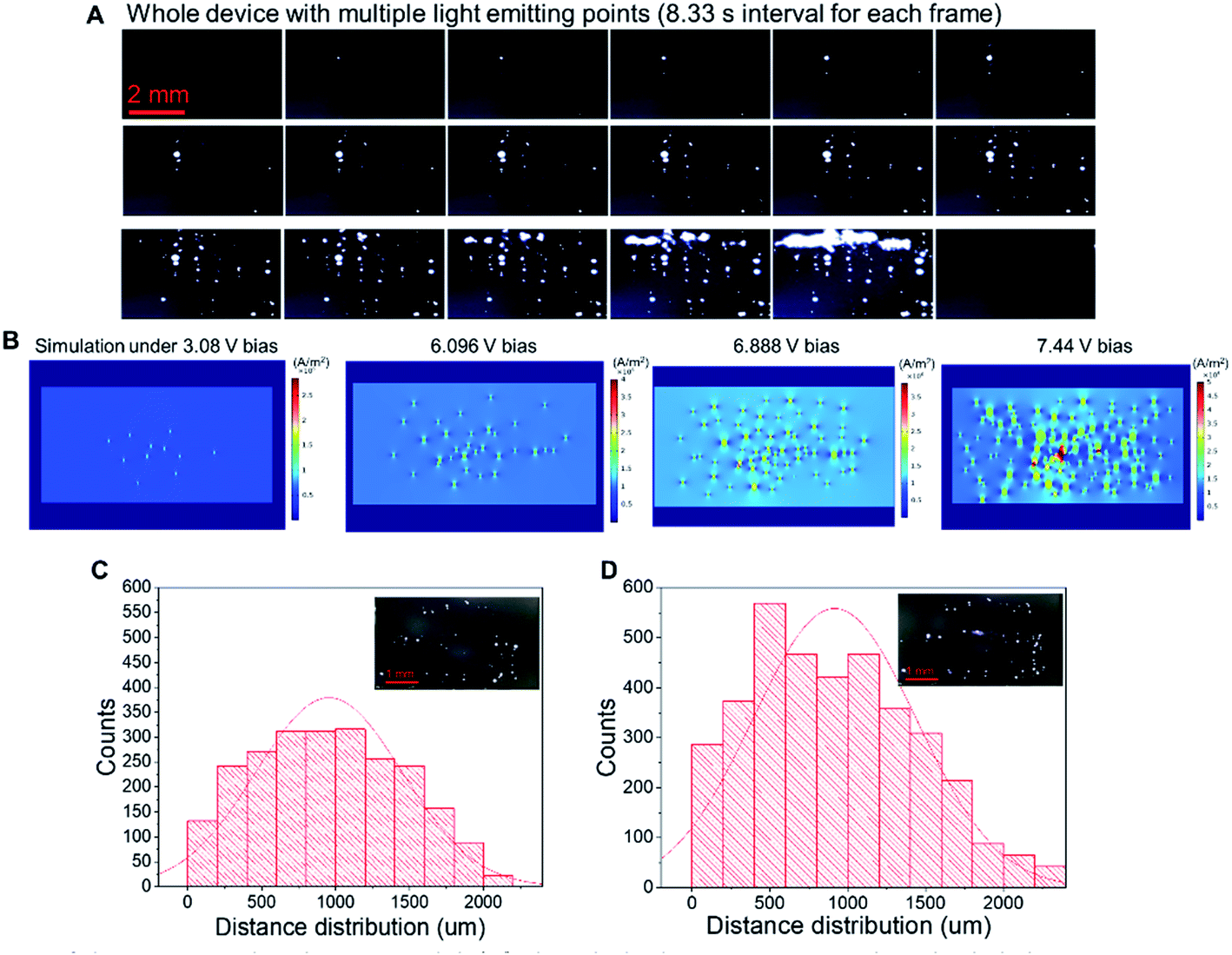 | ||
| Fig. 5 Statistics and verification of the Gaussian distribution model. (A) The whole device vs. time with multiple light emitting points at the increasing driving voltage. (B) The simulated light emitting points at the increasing driving voltage. (C) and (D) are the statistical charts of the distance between each two lighting points from two samples. The inset shows the images of lighting points of LIRGO corresponding to the plots. | ||
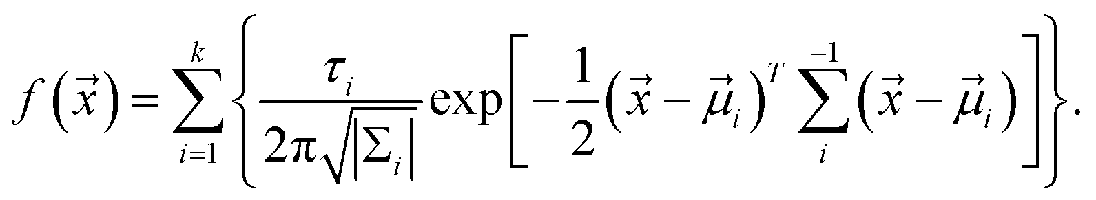
We assume that the distribution of luminescent points conforms to the Gaussian distribution model. Therefore, we defined the formula of the probability density distribution of a light point being found as:
The formula can be represented by several two-dimensional Gaussian components. ![[x with combining right harpoon above (vector)]](https://www.rsc.org/images/entities/i_char_0078_20d1.gif) = (x, y) and refers to the coordinate of the two-dimensional coordinate system. The parameter τi (i = 0, …, k) is the relative proportion of each Gaussian component. The symbol |Σi| represents the determinant of the covariance matrix, ( −
= (x, y) and refers to the coordinate of the two-dimensional coordinate system. The parameter τi (i = 0, …, k) is the relative proportion of each Gaussian component. The symbol |Σi| represents the determinant of the covariance matrix, ( − ![[small mu, Greek, vector]](https://www.rsc.org/images/entities/i_char_e0e9.gif) i)T refers to the transpose of the vector, and Σi−1 denotes the inverse of the covariance matrix. We counted and plotted the distance between every two illuminating points of two samples to verify this formula (Fig. 5C and D). The mean value of the distance between lighting points in Fig. 5C and D is 955 μm and 915 μm, respectively. The experimental results of the statistical analysis demonstrate the random distribution of the luminescent points, which validates the mechanism of LIRGO EL afore-mentioned.
i)T refers to the transpose of the vector, and Σi−1 denotes the inverse of the covariance matrix. We counted and plotted the distance between every two illuminating points of two samples to verify this formula (Fig. 5C and D). The mean value of the distance between lighting points in Fig. 5C and D is 955 μm and 915 μm, respectively. The experimental results of the statistical analysis demonstrate the random distribution of the luminescent points, which validates the mechanism of LIRGO EL afore-mentioned.
Exploration of application
Under vacuum, the LIRGO device emits stable and bright visible light. However, the oxygen and the water molecules present in the air can oxidize and rapidly degrade the device. Its light emission stability is also limited by high temperatures and high currents. In order to improve LIRGO's lifetime in air, we have studied different packaging methods (Fig. 6A). The devices were tested in ordinary air and air depleted of water. For both ordinary air and dry air, 5 sets of experiments were conducted. The mean lifetime is 36 seconds in ordinary air and 236 seconds in dry air (Fig. S11†).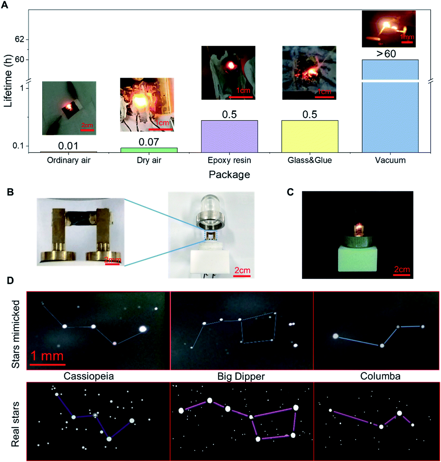 | ||
| Fig. 6 Packaging and applications of LIRGO. (A) The lifetime of emission vs. the package methods of LIRGO. (B) Structure of the LIRGO bulb. (C) LIRGO bulb emits bright light. (D) Constellations of Cassiopeia, Big Dipper and Columba mimicked with LIRGO devices. | ||
In the epoxy package, LIRGO can illuminate. However, epoxy begins to smoke after a few minutes. Thereafter, the device started to flicker, which made it difficult to accurately record the time. We conducted this experiment only for 30 minutes. To prevent oxidation, we glued LIRGO between two glass sheets. However, the glue begins to melt and the device starts flickering after 30 minutes of illumination.
Therefore, illumination in a vacuum is the most stable and feasible currently. In fact, oxidation and heat dissipation are challenges that commercial LEDs need to face as well. For example, the packaging of ordinary light-emitting diodes also requires a vacuum to isolate oxygen and water molecules and good heat dissipation structures to cool down.12 In addition, the illumination is also measured under vacuum in some similar studies.29,31
Moreover, LIRGO has good luminescence repeatability. As LIRGO is not damaged during illumination with an appropriate voltage, the light points will illuminate again in the same place when repowering. After stabilization of the current, the spectra of LIRGO vs. repowering in different runs are recorded in Fig. S12.† There is no significant change in the spectrum and therefore efficiency in different runs.
To verify the practicality of the vacuum package, the design of the LIRGO bulb is demonstrated in Fig. 6B. The LIRGO device is placed in a vacuumed bulb made of polymathic methacrylate (PMMA) and can illuminate steadily (Fig. 6C). In addition, Fig. 6D shows an interesting and ornamental demonstration using randomly distributed lighting points on LIRGO to mimic constellations. The mimicked Cassiopeia using LIRGO is fairly similar to the real Cassiopeia. Big Dipper and Columba are also good examples to prove that LIRGO can mimic star patterns.
Conclusions
This work provides a simple and effective method to make a graphene-based flexible LED. We demonstrate the possibility to tune LIRGO's bandgaps by laser modulation and use LIRGO for micron-sized light sources with adjustable luminescence colours. When the vacuum is 0.02 Pa, and the drive current is 0.01 A, the LIRGO LED with a lifetime higher than 60 hours and a WPE of up to 1.4% is achieved. Four-pad measurements proved LIRGO's non-polarity emission. The current–voltage curves of LIRGO measured are in concordance with the Poole–Frenkel model. A theoretical model of semi-rGO emission is established and explains the random distribution of luminous points. The lifetimes of LIRGO in different packages were tested and the LIRGO bulb was demonstrated for practicality. Finally, we show the possibility of “mimicking” patterns of stars. These experimental results indicate the enormous potential application of the new LIRGO light source.Experimental
Fabrication and measurements
The GO solution (XFNANO Inc.) was spread on the substrate (such as PET, polyimide, heat-resistant paper, etc). After the GO dried, a 448 nm laser with 25 to 40 mW cm−2 power was used to convert GO into LIRGO. The silver electrodes were deposited on both sides of LIRGO and wires were attached to the electrodes.Characterization
The XPS measurements were performed with an X-ray photoelectron spectrometer (PHI Quantera II, Ulvac-Phi Inc.). Raman tests were performed on a laser confocal Raman spectrometer (HR-800, Horiba Inc.). SEM images were recorded with a field emission scanning electron microscope (Quanta FEG 450, FEI Inc.). The LIRGO and GO films were loaded onto a micro-grid, and TEM images were recorded using a field emission transmission electron microscope (JEM-2100F, JEOL).Simulation details
Based on the experimental data, we performed a finite element analysis using Comsol Multiphysics to simulate the relationship between the electro-optical conversion of LIRGO and the external field. The simulation process considers Ohm's law and Kirchhoff's current law. We built a random resistance distribution network. Each resistor unit represents a semi-rGO flake. The sheet resistance of each resistor unit follows the Gaussian distribution, Rij ∼ Nij(μ, σ2). When the local current of a resistor unit reaches a certain threshold, the electrical characteristics of the resistor unit are set to change in order to be consistent with the nonlinear trend of the Poole–Frenkel model. After the electric field is applied, some locations showed a greater current density. When the current density of a certain resistor unit is greater than 0.01 A, the certain resistor sheet is defined as a light-emitting point position. When the voltage is increased, the number of luminous points will increase. More and more resistance units become new light-emitting points and combine to form bigger light points.Calculation details of WPE
The LIRGO is placed flat in the vacuum chamber. The light intensity meter is placed above the LIRGO. The radiated optical power (Popt) on the upper hemisphere of LIRGO can be described as below:where r represents the distance from the light source to the probe of the light intensity meter, and Ie represents the radiant intensity. Meanwhile, the operating voltage (V) and current (C) can be obtained from the source meter. So the total electric power (Pin) is calculated as below:
| Pin = VC |
Finally, its WPE can be obtained as below:
Measurement details
Currents, voltages, spectra, lifetimes, and recordings of luminescence were tested in a vacuum chamber of 0.02 Pa. The values of luminescence intensity were measured using a PM100D frame and an S130C probe from Thorlabs Inc. The measurements of the intensity distribution of the full spectrum with an increasing voltage were carried out using a Maya2000PRO and a USB2000+ provided by Ocean Optics Inc. The current vs. the change of the vacuum pressure was recorded using a Keithley 2636A.Conflicts of interest
There are no conflicts to declare.Acknowledgements
We thank H. Yang and C. Liu from Institute of Semiconductor, CAS for the help in measurements, Y. Mao and J. Zhang from Tsinghua University for the helpful discussion, Tsinghua Nanofabrication Technology Centre and Beijing Innovation Centre for Future Chips for the help in measurements. This work was supported by the National Key R&D Program (2016YFA0200400), National Basic Research Program (2015CB352101), and National Natural Science Foundation of China (61874065, 51861145202, 61574083, and 61434001). The authors are also thankful for the support of the Start-up Funding from Tsinghua University (533306001), Research Fund from Beijing Innovation Centre for Future Chip, the Independent Research Program of Tsinghua University (2014Z01006) and the Shenzhen Science and Technology Program (JCYJ20150831192224146). G. Jiang appreciates the support of Qingfeng Scholarship from Tsinghua University. H. Tian appreciates the support from the Young Elite Scientists Sponsorship Program by CAST (2018QNRC001).References
- W. S. Wong and A. Salleo, Flexible Electronics: Materials and Applications, 2009 Search PubMed.
- G. Fiori, F. Bonaccorso, G. Iannaccone, T. Palacios, D. Neumaier, A. Seabaugh, S. K. Banerjee and L. Colombo, Nat. Nanotechnol., 2014, 9, 768–779 CrossRef CAS PubMed.
- Y. Sun and J. A. Rogers, Adv. Mater., 2007, 19, 1897–1916 CrossRef CAS.
- M. Stoppa and A. Chiolerio, Sensors, 2014, 14, 11957–11992 CrossRef CAS PubMed.
- R.-P. Xu, Y.-Q. Li and J.-X. Tang, J. Mater. Chem. C, 2016, 4, 9116–9142 RSC.
- S.-M. Lee, J. H. Kwon, S. Kwon and K. C. Choi, IEEE Trans. Electron Devices, 2017, 64, 1922–1931 CAS.
- J.-S. Park, H. Chae, H. K. Chung and S. I. Lee, Semicond. Sci. Technol., 2011, 26, 034001 CrossRef.
- J. S. Lewis and M. S. Weaver, IEEE J. Sel. Top. Quantum Electron., 2004, 10, 45–57 CrossRef CAS.
- G. Destriau, Philos. Mag., 1947, 38, 700–739 Search PubMed.
- N. Narendran, Y. Gu, J. P. Freyssinier-Nova and Y. Zhu, Phys. Status Solidi A, 2005, 202, R60–R62 CrossRef CAS.
- S. Pimputkar, J. S. Speck, S. P. DenBaars and S. Nakamura, Nat. Photonics, 2009, 3, 179–181 CrossRef.
- J.-S. Wang, C.-C. Tsai, J.-S. Liou, W.-C. Cheng, S.-Y. Huang, G.-H. Chang and W.-H. Cheng, Microelectron. Reliab., 2012, 52, 813–817 CrossRef CAS.
- Y. H. Tak, K. B. Kim, H. G. Park, K. H. Lee and J. R. Lee, Thin Solid Films, 2002, 411, 12–16 CrossRef CAS.
- V. S. Reddy, K. Das, A. Dhar and S. K. Ray, Semicond. Sci. Technol., 2006, 21, 1747–1752 CrossRef CAS.
- K. S. Novoselov, V. I. Fal'ko, L. Colombo, P. R. Gellert, M. G. Schwab and K. Kim, Nature, 2012, 490, 192–200 CrossRef CAS PubMed.
- F. Xia, H. Wang, D. Xiao, M. Dubey and A. Ramasubramaniam, Nat. Photonics, 2014, 8, 899–907 CrossRef CAS.
- F. H. L. Koppens, T. Mueller, P. Avouris, A. C. Ferrari, M. S. Vitiello and M. Polini, Nat. Nanotechnol., 2014, 9, 780–793 CrossRef CAS PubMed.
- J. Shen, Y. Zhu, C. Chen, X. Yang and C. Li, Chem. Commun., 2011, 47, 2580–2582 RSC.
- C.-T. Chien, S.-S. Li, W.-J. Lai, Y.-C. Yeh, H.-A. Chen, I. S. Chen, L.-C. Chen, K.-H. Chen, T. Nemoto, S. Isoda, M. Chen, T. Fujita, G. Eda, H. Yamaguchi, M. Chhowalla and C.-W. Chen, Angew. Chem., Int. Ed., 2012, 51, 6662–6666 CrossRef CAS PubMed.
- Y. Dong, J. Shao, C. Chen, H. Li, R. Wang, Y. Chi, X. Lin and G. Chen, Carbon, 2012, 50, 4738–4743 CrossRef CAS.
- J. Peng, W. Gao, B. K. Gupta, Z. Liu, R. Romero-Aburto, L. Ge, L. Song, L. B. Alemany, X. Zhan, G. Gao, S. A. Vithayathil, B. A. Kaipparettu, A. A. Marti, T. Hayashi, J.-J. Zhu and P. M. Ajayan, Nano Lett., 2012, 12, 844–849 CrossRef CAS PubMed.
- D. A. Kim, J. H. Shim and N. H. Cho, Appl. Surf. Sci., 2004, 234, 256–261 CrossRef CAS.
- C. Sun, M. T. Wade, Y. Lee, J. S. Orcutt, L. Alloatti, M. S. Georgas, A. S. Waterman, J. M. Shainline, R. R. Avizienis, S. Lin, B. R. Moss, R. Kumar, F. Pavanello, A. H. Atabaki, H. M. Cook, A. J. Ou, J. C. Leu, Y. H. Chen, K. Asanovic, R. J. Ram, M. A. Popovic and V. M. Stojanovic, Nature, 2015, 528, 534–538 CrossRef CAS PubMed.
- J. H. Choi, A. Zoulkarneev, S. I. Kim, C. W. Baik, M. H. Yang, S. S. Park, H. Suh, U. J. Kim, H. Bin Son, J. S. Lee, M. Kim, J. M. Kim and K. Kim, Nat. Photonics, 2011, 5, 763–769 CrossRef CAS.
- D. Yu and L. Dai, Appl. Phys. Lett., 2010, 96, 143107 CrossRef.
- F. T. Vasko and O. G. Balev, Phys. Rev. B, 2010, 82 Search PubMed.
- S. Zhao, L. Rondin, G. Delport, C. Voisin, U. Beser, Y. Hu, X. Feng, K. Muellen, A. Narita, S. Campidelli and J. S. Lauret, Carbon, 2017, 119, 235–240 CrossRef CAS.
- B. V. Senkovskiy, M. Pfeiffer, S. K. Alavi, A. Bliesener, J. Zhu, S. Michel, A. V. Fedorov, R. German, D. Hertel, D. Haberer, L. Petaccia, F. R. Fischer, K. Meerholz, P. H. M. van Loosdrecht, K. Lindfors and A. Grueneis, Nano Lett., 2017, 17, 4029–4037 CrossRef CAS PubMed.
- M. C. Chong, N. Afshar-Imani, F. Scheurer, C. Cardoso, A. Ferretti, D. Prezzi and G. Schull, Nano Lett., 2018, 18, 175–181 CrossRef CAS PubMed.
- H. R. Barnard, E. Zossimova, N. H. Mahlmeister, L. M. Lawton, I. J. Luxmoore and G. R. Nash, Appl. Phys. Lett., 2016, 108, 131110 CrossRef.
- M. Freitag, H.-Y. Chiu, M. Steiner, V. Perebeinos and P. Avouris, Nat. Nanotechnol., 2010, 5, 497–501 CrossRef CAS PubMed.
- R. Beams, P. Bharadwaj and L. Novotny, Nanotechnology, 2014, 25 Search PubMed.
- L. M. Lawton, N. H. Mahlmeister, I. J. Luxmoore and G. R. Nash, AIP Adv., 2014, 4, 087139 CrossRef.
- Y. D. Kim, H. Kim, Y. Cho, J. H. Ryoo, C.-H. Park, P. Kim, Y. S. Kim, S. Lee, Y. Li, S.-N. Park, Y. S. Yoo, D. Yoon, V. E. Dorgan, E. Pop, T. F. Heinz, J. Hone, S.-H. Chun, H. Cheong, S. W. Lee, M.-H. Bae and Y. D. Park, Nat. Nanotechnol., 2015, 10, 676–681 CrossRef CAS PubMed.
- X. Wang, H. Tian, M. A. Mohammad, C. Li, C. Wu, Y. Yang and T. L. Ren, Nat. Commun., 2015, 6, 7767 CrossRef CAS PubMed.
- S. Pei and H.-M. Cheng, Carbon, 2012, 50, 3210–3228 CrossRef CAS.
- A. Mathkar, D. Tozier, P. Cox, P. Ong, C. Galande, K. Balakrishnan, A. L. M. Reddy and P. M. Ajayan, J. Phys. Chem. Lett., 2012, 3, 986–991 CrossRef CAS PubMed.
- F. Yavari, C. Kritzinger, C. Gaire, L. Song, H. Gullapalli, T. Borca-Tasciuc, P. M. Ajayan and N. Koratkar, Small, 2010, 6, 2535–2538 CrossRef CAS PubMed.
- E. Matioli, S. Brinkley, K. M. Kelchner, Y.-L. Hu, S. Nakamura, S. DenBaars, J. Speck and C. Weisbuch, Light: Sci. Appl., 2012, 1 Search PubMed.
- H. Uoyama, K. Goushi, K. Shizu, H. Nomura and C. Adachi, Nature, 2012, 492, 234–238 CrossRef CAS PubMed.
- M. Pope, P. Magnante and H. P. Kallmann, J. Chem. Phys., 1963, 38, 2042–2043 CrossRef CAS.
- R. Mach and G. O. Muller, Phys. Status Solidi A, 1982, 69, 11–66 CrossRef CAS.
- R. Withnall, J. Silver, P. G. Harris, T. G. Ireland and P. J. Marsh, J. Soc. Inf. Disp., 2011, 19, 798–810 CrossRef CAS.
- S. Berciaud, M. Y. Han, K. F. Mak, L. E. Brus, P. Kim and T. F. Heinz, Phys. Rev. Lett., 2010, 104, 227401 CrossRef PubMed.
- N. T. Gordon, IEEE Trans. Electron Devices, 1981, 28, 434–436 Search PubMed.
- S. Park, J. An, J. R. Potts, A. Velamakanni, S. Murali and R. S. Ruoff, Carbon, 2011, 49, 3019–3023 CrossRef CAS.
- K. Tang, F. Zhu, Y. Li, K. Duan, S. Liu and Y. Chen, 2014.
Footnotes |
| † Electronic supplementary information (ESI) available. See DOI: 10.1039/c9na00550a |
| ‡ These authors contributed equally to this work. |
| This journal is © The Royal Society of Chemistry 2019 |