
 Open Access Article
 This Open Access Article is licensed under a Creative Commons Attribution-Non Commercial 3.0 Unported Licence
Observing growth under confinement: Sn nanopillars in porous alumina templates†
Gary S.
Harlow
 *a,
Jakub
Drnec
b,
Tim
Wiegmann
b,
Weronica
Lipé
a,
Jonas
Evertsson‡
a,
Axel R.
Persson
c,
Reine
Wallenberg
c,
Edvin
Lundgren
a and
Nikolay A.
Vinogradov
*d
*a,
Jakub
Drnec
b,
Tim
Wiegmann
b,
Weronica
Lipé
a,
Jonas
Evertsson‡
a,
Axel R.
Persson
c,
Reine
Wallenberg
c,
Edvin
Lundgren
a and
Nikolay A.
Vinogradov
*d
aDivision of Synchrotron Radiation Research, Lund University, 221 00 Lund, Sweden. E-mail: gary.harlow@sljus.lu.se
bESRF – The European Synchrotron, 71 Avenue des Martyrs, 38000 Grenoble, France
cNational Center for High Resolution Electron Microscopy and NanoLund, Lund University, 221 00 Lund, Sweden
dMAX IV Laboratory, 22594, Lund, Sweden. E-mail: nikolay.vinogradov@maxiv.lu.se
First published on 29th October 2019
Abstract
Using a micro-focused high-energy X-ray beam, we have performed in situ time-resolved depth profiling during the electrochemical deposition of Sn into an ordered porous anodic alumina template. Combined with micro-diffraction we are able to follow the variation of the structure at the atomic scale as a function of depth and time. We show that Sn initially deposits at the bottom of the pores, and forms metallic nanopillars with a preferred [100] orientation and a relatively low mosaicity. The lattice strain is found to differ from previous ex situ measurements where the Sn had been removed from the porous support. The dendritic nature of the pore bottom affects the Sn growth mode and results in a variation of Sn grain size, strain and mosaicity. Such atomic scale information of nano-templated materials during electrodeposition may improve the future fabrication of devices.
1 Introduction
Traditional methods of nano- and micro-fabrication are largely lithographic (i.e. material is cut away). There is, however, great interest in alternate techniques for nanoscale manufacturing.1 Electrochemical deposition is one such method, where devices are grown atom-by-atom, from the bottom up.2,3 Often a template is used to guide and restrict the growth of nanowires and other nanostructures,4 but relatively little is understood about the impact that template dimensions have on crystallographic orientation and strain during growth. Control and knowledge of such crystallographic parameters is known to be essential for creating and improving nanoscale devices where changes in atomic structure and crystallographic orientation can impact device performance.5,6Porous anodic alumina (PAA), formed by the electrochemical anodization of aluminium in various electrolytes, is a popular template for the fabrication of nanoscale devices such as magnetic storage,7 catalytic membranes,8 batteries, and solar cells.9,10 The distance can be tuned by varying the anodisation voltage, and pore diameters can be chosen between 10 and 400 nm by careful selection of electrolyte composition and voltage.11 Further tuning of the pore diameter can be made by chemically etching the oxide, so-called ‘pore widening’.12 When the anodizing voltage is just below the break-down potential for a given electrolyte, the pores are found to self-organize into a hexagonal arrangement.13 Depending on the anodisation time the PAA film thickness can exceed several tens of micrometers, creating high-aspect ratio templates.14 For improved electrodeposition the PAA can also be separated from the aluminium substrate by chemical etching or reverse polarization/voltage pulsed detachment,15 resulting in a thin membrane that can be coated on one side with a more conductive material than oxide covered aluminium.
Functionalisation of the pores can be carried out via electrodeposition, creating a material with novel properties.4 Subsequently, the PAA template can then be removed leaving free standing ordered nanostructures such as particles or wires on the substrate.16,17 Metallic Sn nanopillars or nanowires grown electrochemically in PAA represent a well-studied and interesting model system with potential applications. Given the excellent electrical conductivity and corrosion resistance of Sn, which has led to the extensive use of Sn as wires and solders in the electronics industry, one might expect such uses to continue in future nanoscale devices Sn nanowires exhibit unique superconducting and magnetization properties.18 Furthermore, oxidation of Sn to SnO2 can be used to create gas sensors19 and battery electrodes.20 It has been reported that electrodeposition of Sn into PAA creates single-crystalline nanopillars of metallic β-Sn in the pores, such that the [100] crystallographic direction is aligned along the pore length.18,21,22 However, these studies were performed ex situ and required the dissolution of the supporting PAA template. Furthermore, structural changes occurring during the growth and the growth mechanism, which are important for functional optimization, are yet to be assessed. The encapsulating nature of templates such as PAA, as well as the harsh electrochemical environment, make the direct observation of growth processes very difficult. Much of our recent work has focused on developing synchrotron-based X-ray techniques to study such systems. We previously performed in situ grazing-incidence transmission small angle X-ray scattering (GTSAXS) experiments during the formation of PAA, allowing us to follow the growth and ordering of PAA.23,24 We have also used X-ray absorption near edge structure spectroscopy (XANES) to determine that electrodeposited Sn nanopillars are metallic, and X-ray fluorescence (XRF) to follow the overall deposition, and GTSAXS to follow the growth.25 These techniques, however, did not provide information about the position of the deposit within the pores or it's atomic structure.
In this contribution, we make use of the relatively recent availability of high-energy focused X-ray beams and modern highly sensitive large area detectors.26–28 The electrodeposition of Sn into a 18.5 μm-thick PAA template is observed by scanning the sample through a 70 keV X-ray beam with a vertical beam height of 5 μm. The high energy allows the beam to penetrate through the sample and reduces the dimensions of reciprocal space such that whole diffraction rings out to a large angle can be recorded in a single detector acquisition. Using this technique we obtain spatially and temporally resolved information about the evolution of the structural parameters and the morphology of the electrodeposited Sn. The metallic Sn is shown to be initially deposited at the bottom of the pores, continuously filling the pores towards the surface of the PAA and forming Sn metallic nanopillars, composed of small strained crystallites with a [100] orientation along the direction perpendicular to the PAA film. The strain in the template-confined nanopillars is found to be different from previous ex situ measurements. A small number of pores are filled preferentially, after these pores fill to the top of the oxide an amorphous Sn-containing layer is formed on top of the PAA film.
2 Experimental methods
Nanoporous anodic aluminium oxide samples for electrodeposition were prepared by serial anodisation of mirror-polished polycrystalline Al (purity 99.95%, from Goodfellow, Inc.) at 40 V in a 0.3 M solution of oxalic acid. The length of the second anodisation step that produced the PAA template was 6.5 hours which results in pore radii of around 20 nm and length (depth) of ∼18.5 μm.Prior to the deposition of Sn the barrier oxide layer, between the pore bottom and the aluminium substrate, was thinned by a voltage reduction process for the purpose of subsequent electrodeposition.29 Metallic Sn was then deposited into the porous substrate from a 0.15 M solution of SnSO4 in 0.1 MH2SO4 (20 g l−1 SnSO4 and 10 g l−1 H2SO4), at room temperature, using an alternating potential of 15 VRMS at 400 Hz. The same electrochemical cell was used for both the anodisation of aluminium samples and Sn electrodeposition but cleaned between the processes by running excess electrolyte through the cell. The detailed description of the electrochemical cell and our anodisation/electrodeposition apparatus can be found in our previous papers.23–25 The schematics of the experiment are shown in Fig. 1.
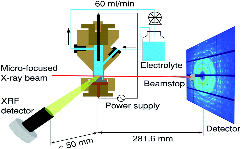 | ||
| Fig. 1 Schematics of the experiment conducted at the high-energy beamline, ID31, at ESRF. The sample was continuously scanned in the 5 μm X-ray beam (red line) providing spatially and temporally resolved information about the electrodeposited Sn. The schematics includes the X-ray fluorescence detector, electrochemical flow cell30 as well as a large area XRD detector. | ||
To follow the structural evolution of the electrodeposited Sn into the PAA, X-ray diffraction (XRD) patterns and Kα XRF was measured while vertically stepping the sample through a micro-focused synchrotron X-ray beam. These height scans were performed in loops going from a minimum sample height with respect to the beam (a negative probing depth where the X-ray beam is above the sample) to maximum sample height (the X-ray beam passes through the sample at a certain depth) and back. The scan step was 4 μm, and the duration of one scan loop was ∼120 s, giving an average temporal resolution of 60 s for each probing depth.
The in situ XRD and XRF experiments were performed at beamline ID31 at The European Synchrotron Radiation Facility (ESRF). A 70 keV (λ = 0.17712 Å) X-ray beam, focused to ∼5(v) × 20(h) μm, was impinged on the sample parallel to the surface, at a very glancing angle, below 0.1°. A large area detector Pilatus3 X CdTe 2M from Dectris was placed 281.6 mm downstream. A 5 mm tungsten beamstop was used to block the direct beam and prevented the detector from saturation. In such geometry the Q-range was between 0.6 Å−1 and 38 Å−1 with resolution of 0.02 Å−1. The azimuthal integrations of the 2D images to 1D patterns were done with pyFAI software package.31 The 2D images were normalized by the beam monitor value prior to integration.
Simultaneously while recording XRD patterns, XRF was measured using a Vortex-EM 300 detector (SII Nano Technology USA Inc.), and respective Sn XRF depth profiles were acquired. The detector was calibrated using Sn, Pd and Cu foils (Goodfellow, Inc., purity 99.995%). The XRF detector nozzle was placed ∼50 mm sideways from the electrochemical cell, as depicted in Fig. 1.
Ex situ FIB-SEM measurements were conducted in the Lund Nano Lab using a Nova NanoLab 600 Dual beam (FIB/SEM) from FEI Company to image the pores in the oxide. A trench was cut out in the aluminium oxide with an ion beam of Ga ions to expose the pores within the oxide. The pores were then imaged from the side by secondary electrons from the electron beam, showing the pores and the Sn within. The same system was also used to prepare TEM lamellas, which were transferred to a TEM grid using an ultra sharp probe tip. The lamella prepared was extracted from a similar sample, but where the oxide was only 7 μm thick (it was anodized for 2 hours instead of 6.5 hours). TEM/STEM was measured on a Jeol 3000F microscope operating at 300 kV. For compositional analysis, XEDS (Oxford Instruments X-max, in the TEM) was used.
3 Results and discussion
In Fig. 2 the measured XRF intensity is shown as a function of probing depth. The physical geometry of the X-ray beam with respect to the pores is illustrated by the inset. The small size of the X-ray beam (5 μm) allows the Sn depth profile within the PAA to be measured as a function of deposition time. The sample horizon (top of the PAA over-layer) exposed to the Sn electrolyte is indicated in Fig. 2 with a dashed line. Just before the electrodeposition, a weak Sn XRF signal from the electrolyte is observed above the sample horizon.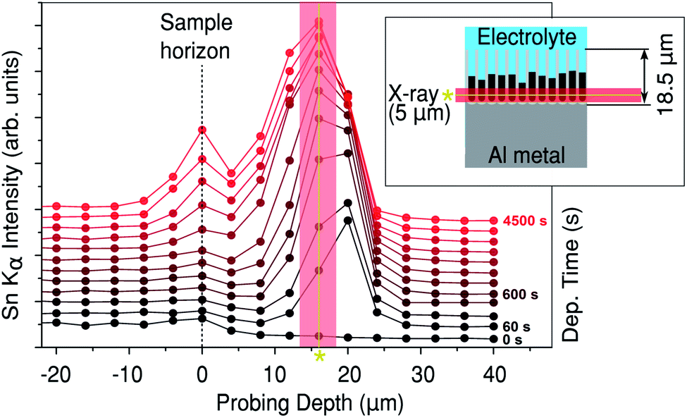 | ||
| Fig. 2 Sn Kα (25.3 keV) XRF against probing depth. The inset shows the geometry of the sample with respect to the beam. The time since the start of Sn deposition is indicated on the right. The asterisk/solid line indicates approximately the average centre of the peak, where the diffraction in Fig. 3 was measured. | ||
After 60 seconds of Sn electrodeposition (1 measurement cycle), a pronounced Sn XRF signal is observed close to the bottom of the pores. This XRF peak increases in intensity, while its centre shifts towards the sample horizon as the nanopores are filled from the bottom by Sn. The intensity of the Sn XRF peak saturates after 1000 s of deposition. At this point a new XRF peak is observed at negative probing depths (above the sample horizon), indicating that Sn starts to deposit on the PAA surface. The dip between the two XRF peaks suggests there is a void, where most of the pores above a certain point don't contain electrodeposited Sn, this was also confirmed by ex situ scanning electron microscopy (SEM) images of cross-sections cut with a focused ion beam (FIB), see Fig. 6e–f.
To obtain quantitative structural information, XRD patterns were collected simultaneously with the Sn XRF. In Fig. 3 we show three 2D detector images and their respective integrated XRD patterns at different deposition times from a probing depth Δ of 16 μm. This depth corresponds to the in-pore peak position of the Sn XRF as indicated by the asterisk (and solid line) on Fig. 2. Fig. 3a shows the 2D diffraction pattern before the electrodeposition (i.e. t = 0 s). The corresponding XRD curve from which the background (red line in the inset) has been subtracted in order to facilitate the indexing of the diffraction peaks. The inset in Fig. 3a shows the full XRD pattern prior to background subtraction. Note that only 2θ-angles between 2.75 and 10.25 degrees (which is equivalent to 24.09 to 101.97 degrees for Cu Kα) were used for the indexing.
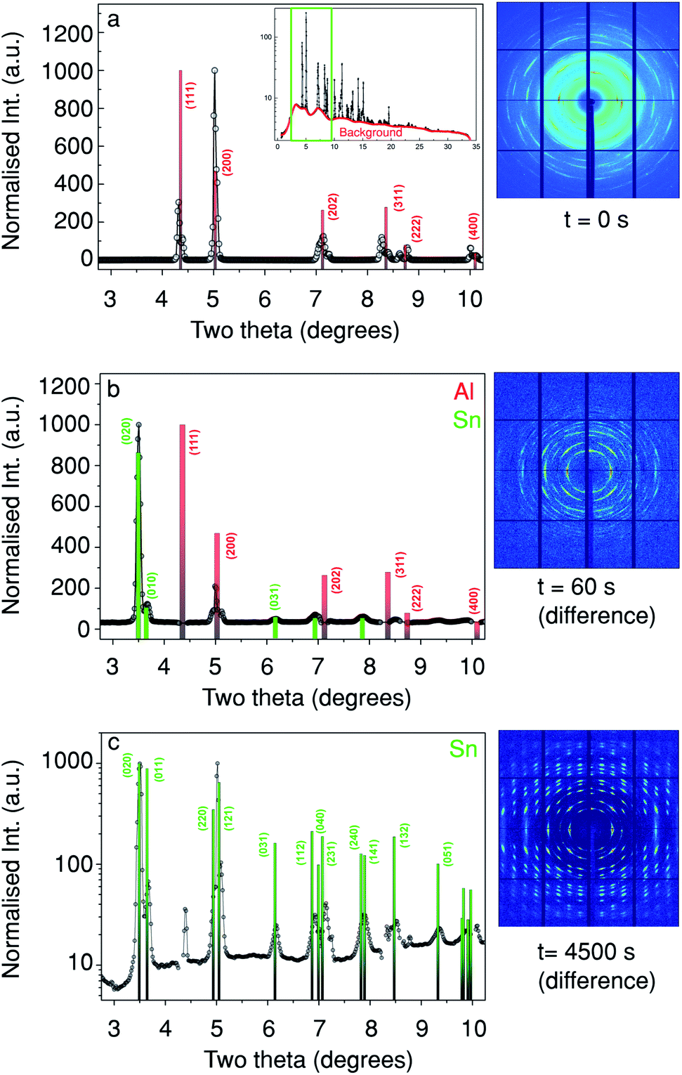 | ||
| Fig. 3 The evolution of the diffraction pattern at a probing depth of 16 μm as indicated in Fig. 2(a–c) show the azimuthally-integrated intensity from the detector (2θ-plots), while the adjacent images show the respective diffraction patterns. (a) Before Sn deposition, (b) after 60 s of Sn deposition (with 0 s subtracted), (c) after 4500 s of Sn deposition (deposition end, also with 0 s subtracted), c is plotted with a log scale to make the weaker peaks at higher angles more visible. Note that the [010] and [100] directions are equivalent for this unit cell. | ||
The XRD pattern at t = 0 s (Fig. 3a) is dominated by face-centred cubic Al diffraction peaks.32 In Fig. 3b we show a 2D diffraction pattern taken at t = 60 s, (after subtraction of the 2D diffraction pattern taken at t = 0 s, Fig. 3a). From the respective XRD curve in Fig. 3b it is clear that a number of new diffraction peaks are present, the most intense were found at 2θ = 3.5° corresponding to β-Sn (020) and β-Sn (121) at 2θ = 5.0°. These peaks match tabulated values well,32 note that the [010] and [100] directions are equivalent in this unit cell and for the rest of the paper the directions have been switched to aid the interpretation. Fig. 3c shows the change in the diffraction pattern and the respective XRD curve after 4500 s of Sn deposition, again matching a β-Sn phase as in Fig. 3b. Moreover, the absence of Sn powder rings suggests a low mosaicity and a preferred orientation in the deposited material. This is in agreement with previous ex situ studies.33
In Fig. 4a a comparison of the Sn XRF and the Sn (200) diffraction signals is presented. Fig. 4a–c show depth profiles of the Sn content in the sample at three different electrodeposition stages: just before the deposition, (Fig. 4a); after 60 s of deposition, (Fig. 4b); and after 4500 s of deposition, (Fig. 4c). Note that the Sn XRF signal corresponds to any Sn present in the sample, irrespectively of its structure or oxidation state, whereas the intensity of Sn (200) diffraction signal is only determined by the amount and order of crystalline Sn present.
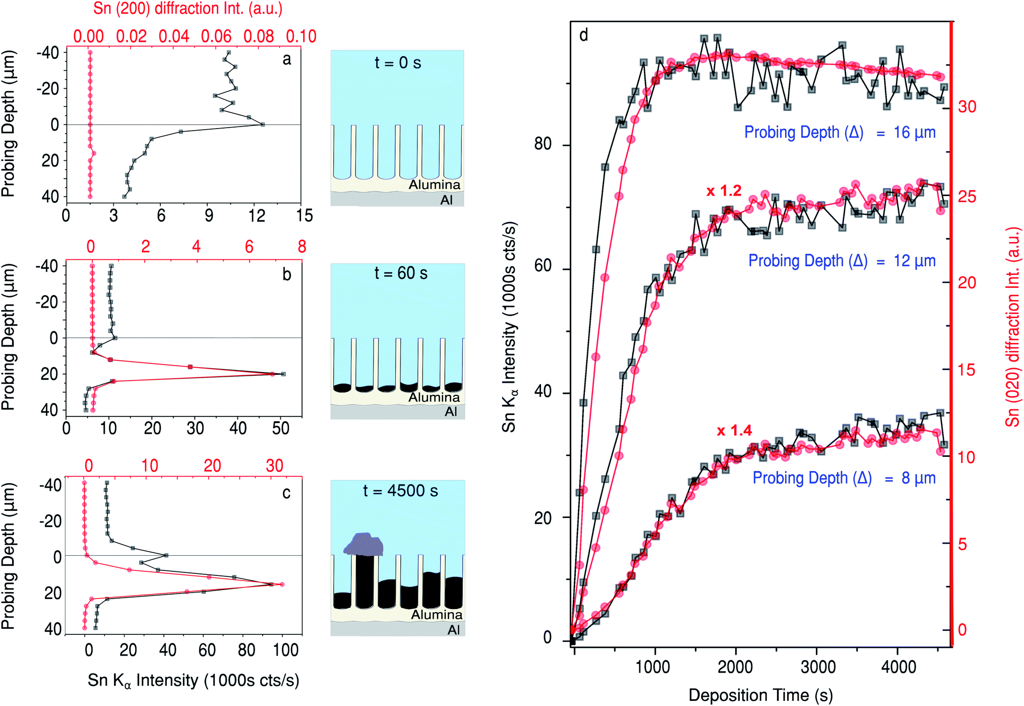 | ||
| Fig. 4 Comparison between the Sn XRF and the Sn (200) diffraction peak intensity at different deposition stages vs. sample height (a–c), and at different sample heights vs. deposition time (d). Note that sample height is defined such that the sample surface lies at 0 and the positive direction is into the pores. The schematics (a–c) illustrate the morphology of the sample at the respective deposition stage. | ||
Before the electrodeposition starts, there is no crystalline Sn present, so no intensity above background is measured for the β-Sn (200) Bragg reflection at time t = 0 s (Fig. 4a). There is, however, a background XRF signal that comes from Sn ions in the electrolyte prior to the deposition. The measured background XRF follows the local concentration of Sn ions in the solution, dropping when the sample displaces the electrolyte at positive probing depths. After 60 s of deposition, pronounced peaks are observed in both the XRF and XRD signals at a probing depth close to the pore bottoms. The pore length deduced from these X-ray measurement is close to the 18.5 μm measured using ex situ FIB-SEM (Fig. 6e). Therefore, Sn electrodeposition in the PAA template starts with the formation of metallic Sn at the bottom of the pores. As more Sn is deposited into the pores, both the XRF and XRD (200) peaks broaden (as function of probing depth) and shift towards smaller Δ values, closer to the sample surface, indicating filling of the pores with crystalline Sn. In the later stages of Sn deposition the XRF signal reveals the presence of another XRF peak centred at Δ = 0 μm, that is at the sample surface (Fig. 4c). Interestingly the XRD signal stays at a background level, suggesting the formation of a different Sn phase. Moreover, as shown in Fig. 5h at Δ = 0 μm there is an absence of any strong diffraction peaks other than traces of β-Sn signatures. This small signal most likely originates from the longest metallic Sn nanopillars that extend to the sample surface. Therefore close to the sample surface the Sn deposits are not in a β-Sn phase like inside the pores, but in a different Sn-based phase which is detected by the XRF signal but not by the diffraction. We also observe such deposits in ex situ SEM images of the sample surface (Fig. S1†). Furthermore, in Fig. S2† diffuse scattering rings are clearly visible in the difference between the last and the first images shown. The presence of the diffuse scattering rings in Fig. 5h is likely another signature of a less ordered Sn phase on top of the PAA. We must remark, however, that this could be explained by other effects such as dissolution of the PAA matrix.
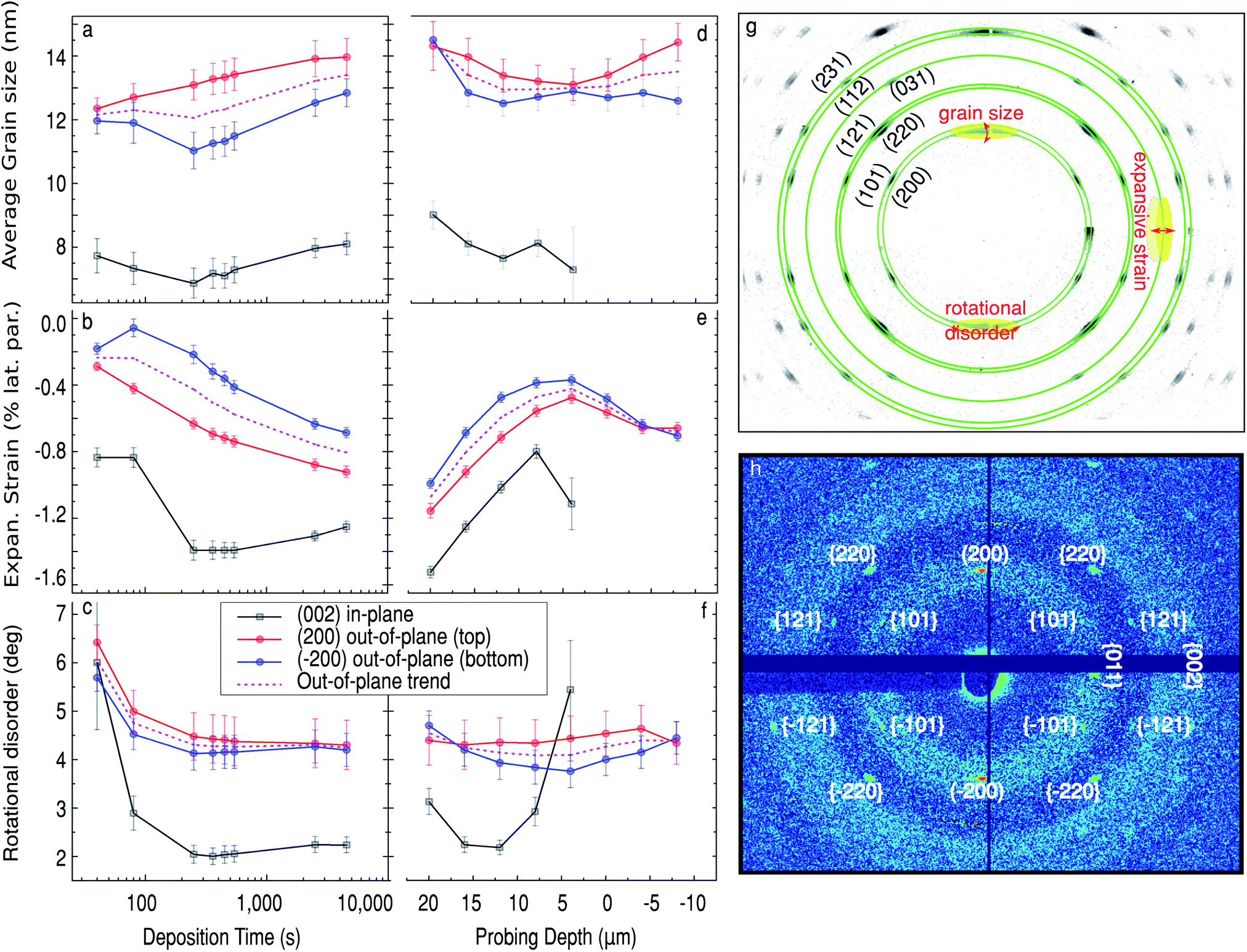 | ||
| Fig. 5 Time evolution of Sn nanowires structural parameters during the deposition at Δ = 16 μm (a–c), and along the pore after the deposition, t = 4500 s (d–f). Black squares show the in-plane data obtained from analysing two symmetry-equivalent reflections of the (002) family. Red and blue circles correspond to the out-of-plane data obtained from analysing (200) and (−200) reflections (top and bottom, respectively) of the {200} family. The dashed pink curve shows the mean value for the out-of-plane data. (g) Diagram showing how the structural information is extracted from the diffraction pattern. (h) Diffraction pattern at the top of the oxide, mostly showing a weak Sn diffraction signature from longer nanopillars. | ||
Whereas Fig. 4a–c demonstrate the depth profiles of Sn concentration in the sample, Fig. 4d compares Sn XRF and XRD signals as a function of deposition time. At all positions the signals increase at the beginning of the deposition and plateau at later stages of the Sn deposition. It is clear that both the XRF and XRD signals saturate sooner in measurements close to the bottom of the pores. The rate of increase for both signals is lower at Δ = 12 μm, and even lower at 8 μm. Since the PAA layer is 18.5 μm thick, at 16 μm the 5 ± 0.5 μm beam will probe approximately the first 5 μm of the pores and the (200) diffraction signal saturates at 1025 ± 225 s, this yields an initial deposition rate of 4.88 ± 0.32 nm s−1.
To obtain atomic scale information about the growth of Sn nanopillars, such as average in- and out-of-plane crystallite (coherent grain) sizes, lattice strain and the mosaicity (corresponding to the in-plane ‘twist’ and out-of-plane ‘tilt’ rotations), we have analysed the position and shape of the Sn diffraction signatures. The details of the data extraction procedure are given in the ESI† and illustrated in Fig. 5g. The in-plane direction has been defined to be parallel to the sample surface, and the in-plane structural parameters were obtained from the (002) diffraction spot, shown in Fig. 5g. Out-of-plane parameters were derived from two symmetry-equivalent (top and bottom) Sn (200) reflections. The out-of-plane trend, was calculated as the average of the latter. The temporal and spatial variation of these parameters are summarized in Fig. 5b–g. Fig. 6a–d show transmission electron microscopy (TEM) images of a lamella extracted via FIB from a similarly prepared sample (with shorter pores) which compliments our interpretation of the X-ray data.
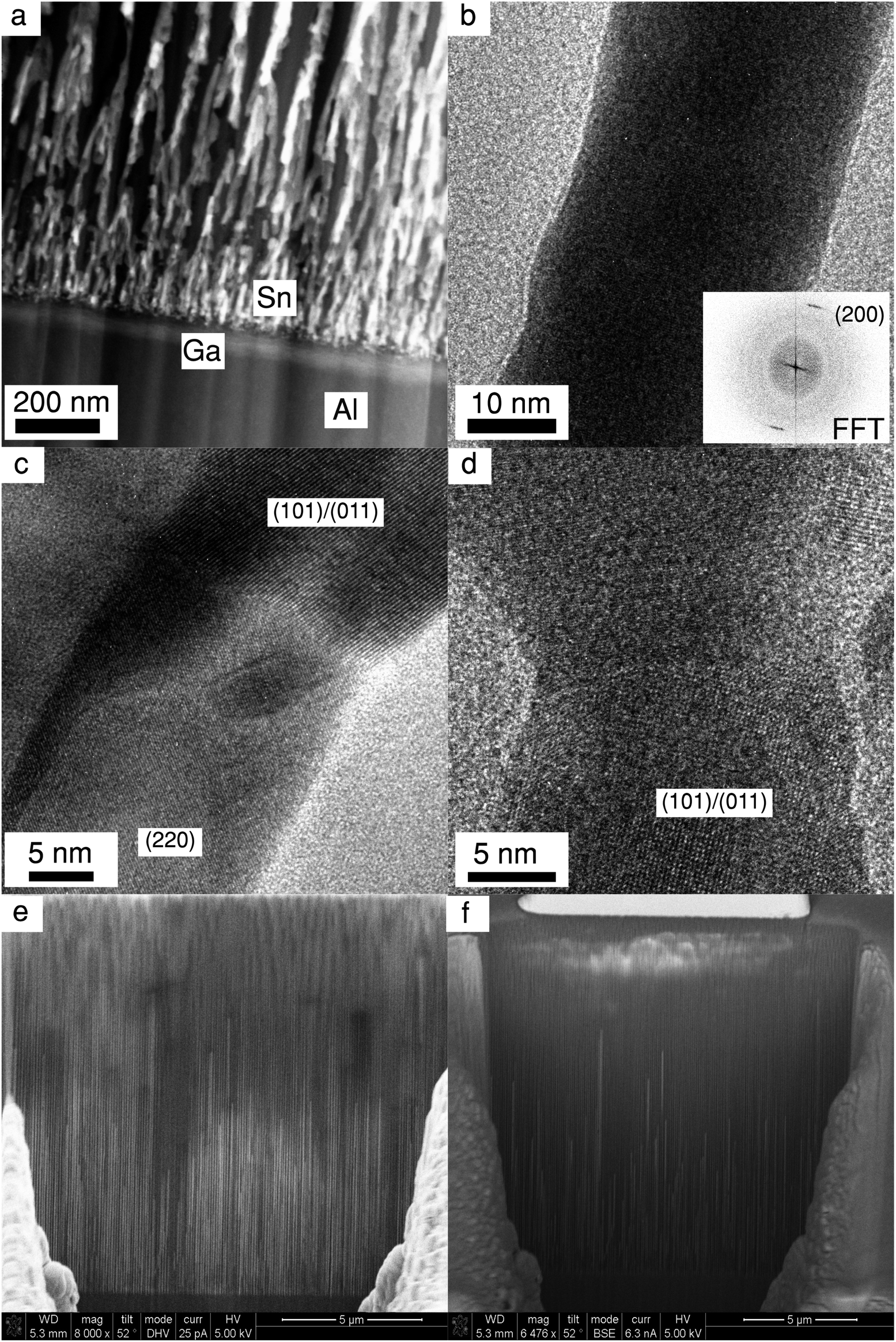 | ||
| Fig. 6 Ex situ transmission electron microscopy from a FIB lamella of a similar sample. (a) STEM image showing the branching of the pores, energy-dispersive X-ray spectroscopy (XEDS) was used to identify elements. The Ga band is the result of ion implantation caused by the FIB. (b) TEM from the straight section of a single nanopillar, the inset shows a fast Fourier transform (FFT) of the image. (c) TEM showing a structural transition close to where two branches join. From a FFT, planes with 2.04 Å and 2.77 Å spacing were labelled at (200) and (101) or (011) planes. (d) TEM showing a structural transition close to where a branch joins the main nanopillar. The square pattern at the bottom had a spacing of 2.77 Å which could be either (101) or (011) planes. (e) FIB-SEM cross section of the actual sample used for the X-ray measurments, measured using the down-hole mode of the SEM. (f) The same cross-section but measured in back-scattering mode. | ||
The time evolution of the Sn structural parameters (average grain size, lattice strain and rotational disorder) at the bottom of the Sn deposit is shown in Fig. 5a–f. By measuring at 16 μm the beam profile covers the first 5 μm, of the pores, so that is the branched section and a significant section of ‘straight pores’. The position also corresponds to the average maximum of both the Sn (200) diffraction and Sn XRF signals at Δ = 16 μm, as indicated in Fig. 2. We observe that the in-plane grain size stays nearly constant at around 7.5 nm. There is a small dip in one of the out-of-plane peaks from around 100 s. Based on the calculated deposition rate of 4.88 ± 0.32 nm s−1 and a measured height of the branched pores of 450 ± 50 nm we think this corresponds to the pores filling past the branched dendrite-like pores that are created from stepping down the potential at the end of the anodisation (see Fig. 6a). This step is performed to reduce the thickness of the barrier layer and improve the Sn electrodeposition. Following this the out-of-plane grain size gradually increases from about 12 to 13.5 nm during the electrodeposition.
The Sn nanopillars at Δ = 16 μm have a contracted lattice compared to bulk Sn. After 100 s of deposition, an abrupt increase in the in-plane strain from −0.8% to −1.4% (contraction) begins due to the deposition in the single pores above the branched pores, this reduces slightly to −1.25% towards the end of deposition. The out-of-plane strain on the other-hand progressively increases (contraction), from −0.2% at the beginning to −0.8% at the end of deposition. The presence of a clear transition in the in-plane strain and its absence in the out-of-plane data suggests a clear difference in strain for the more confined branches at the bottom of the pores than the larger diameter single pores.
In Fig. 6c–d, which show where the pore branches meet, there are clear domain boundaries with different atomic arrangements. While atomic resolution was not fully achieved in our TEM measurements (due to the sample being sensitive to the electron beam, hence exact tilting was not possible), some crystallographic fringes are observed and it was possible to identify some of the crystallographic planes visible. The measured spacing of 2.89 Å in Fig. 6b is close to the (200) inter-planar distance. This compliments the X-ray data that also shows a strong (200) peak along the pore direction (i.e. perpendicular to the sample). It must, however, be noted that dark-field imaging suggested a number of pillars with different orientations, although we weren't able to directly image them. This is still consistent with our interpretation as many more nanopillars are sampled by the X-ray measurement.
The rotational disorder in the crystallites forming at the base of the nanopillars is rather high at the beginning of deposition (∼6°) for both in-plane and out-of-plane mosaicity, as seen in Fig. 5c. This is likely due to the branches being rotated from each other having different angles with respect from the substrate. Both the twist and tilt of the Sn nanowires drops rapidly throughout the initial stages of deposition, as more and more branches merge, and starts to plateau at ∼2% for twist and ∼4% for tilt after 100 s of deposition.
The final spatial variation of crystallographic parameters in the Sn nanopillars complements the overall picture obtained. In Fig. 5d–f the structural parameters are shown as a function of position along the pore at t = 4500 s. (Note that the in-plane data for Sn nanopillars from above the surface (Δ ≤ 0) could not be retrieved due to a weak signal-to-noise ratio.) The average in-plane and out-of-plane crystallite size remains rather constant along the formed nanopillar. For both directions we observe a consistent decrease in the strain towards the sample surface, as demonstrated in Fig. 5e. Fig. 5f shows that the tilt (out-of-plane mis-orientation) of the crystallites remains constant along the whole length, while the twist, i.e. in-plane mis-orientation, increases towards the pore opening. The signal observed at and above the sample horizon (Δ ≤ 0) arises from the longest Sn nanopillars that reach the pore opening at the sample surface and the diffraction from the tails of the beam.
To summarize, the pores are filled from the bottom with a metallic β-Sn phase. The bottom of the pores are branched so there is a high degree of in-plane rotational disorder which abruptly decreases when the branches join. At this point there is also a large increase in inward strain. In fact the observation of inward strain is contrary to previous ex situ reports where the Sn metal was removed from the confinement of the pores.21,22 After about 1000 s some pores are fully filled and a structurally different Sn-containing phase forms on top of the PAA. The β-Sn nanopillars are formed with a preferred [100] orientation, as indicated by the (200) reflection being the strongest and lying perpendicular to the sample surface. The nanopillars also exhibit moderate in- and out-of-plane mosaicity (∼2 deg twist and ∼4 deg tilt).
4 Conclusions
In conclusion, we have followed the electrodeposition of metallic Sn into a PAA matrix in situ, using simultaneous micro-focused high-energy XRD and XRF. We confirm that, with the guiding action of the nanopores, highly oriented crystalline β-Sn nanopillars are formed, with the [100] crystallographic direction preferentially ordered along the pores with the growth starting from the bottom. Once the nanopillars grow beyond the pores, an amorphous phase is formed. Contrary to the studies of Shin et al.,21,22 we observed an inward strain in both the in-plane (transverse) and the out-of-plane (longitudinal) direction, rather than a longitudinal lattice expansion. We attribute the observed negative expansion to the confinement action of the pore walls. It may be that the chemical treatment necessary for dissolving the porous alumina template and releasing the Sn nanopillars, causes the relaxation previously reported.21,22 Furthermore, we show how pore branching, which is consequence of the voltage-reduction method of barrier layer thinning, disrupts the crystallographic orientation of electrodeposited nanostructures.The experimental in situ approach used provides new opportunities for understanding electrodeposition into nano-confined structures. We show that changes in the atomic ordering and orientation can be followed during templated electrodeposition. By understanding the impact of template dimensions and shape on nanowires during growth (such as the branching in this study) one can begin to design more effective templates and structures.
The 70 keV X-ray beam allows for easy access to many normally inaccessible X-ray absorption edges, while the focused X-ray beam provides a good spatial resolution for in situ depth profiling and micro-diffraction of electrodeposited materials. This approach should be applicable to deposition inside many different types of templates, offering unique opportunities to observe growth processes under confinement. Future improvements in both temporal and spatial resolution are expected from better focused beams and faster motors.
Conflicts of interest
There are no conflicts to declare.Acknowledgements
The experiments were performed on beamline ID31 at the European Synchrotron Radiation Facility (ESRF), Grenoble, France. The authors would like to thank Helena Isern and Florian Russelo for help with the experimental setup at ESRF ID31 beamline. This work was financially supported by the Swedish Research Council by the Röntgen-Ängström Cluster “In situ High Energy X-ray Diffraction from Electrochemical Interfaces (HEXCHEM)” (project no. 2015-06092). The ex situ microscopy was performed within NanoLund at Lund University.Notes and references
- S. Jesse, A. Y. Borisevich, J. D. Fowlkes, A. R. Lupini, P. D. Rack, R. R. Unocic, B. G. Sumpter, S. V. Kalinin, A. Belianinov and O. S. Ovchinnikova, ACS Nano, 2016, 10, 5600–5618 CrossRef CAS PubMed.
- E. J. Menke, M. A. Thompson, C. Xiang, L. C. Yang and R. M. Penner, Nat. Mater., 2006, 5, 914 CrossRef CAS PubMed.
- P. V. Braun and P. Wiltzius, Adv. Mater., 2001, 13, 482–485 CrossRef.
- Y. Liu, J. Goebl and Y. Yin, Chem. Soc. Rev., 2013, 42, 2610–2653 RSC.
- F. J. Lopez, E. R. Hemesath and L. J. Lauhon, Nano Lett., 2009, 9, 2774–2779 CrossRef CAS PubMed.
- M. Mattila, T. Hakkarainen, M. Mulot and H. Lipsanen, Nanotechnology, 2006, 17, 1580–1583 CrossRef CAS PubMed.
- E. Berganza, C. Bran, M. Jaafar, M. Vázquez and A. Asenjo, Sci. Rep., 2016, 6, 29702 CrossRef PubMed.
- M. Pellin, P. Stair, G. Xiong, J. Elam, J. Birrell, L. Curtiss, S. George, C. Han, L. Iton, H. Kung, M. Kung and H.-H. Wang, Catal. Lett., 2005, 102, 127–130 CrossRef CAS.
- A. B. F. Martinson, J. W. Elam, J. T. Hupp and M. J. Pellin, Nano Lett., 2007, 7, 2183–2187 CrossRef CAS PubMed.
- S. Liu, Z.-R. Tang, Y. Sun, J. C. Colmenares and Y.-J. Xu, Chem. Soc. Rev., 2015, 44, 5053–5075 RSC.
- C. Y. Han, G. A. Willing, Z. Xiao and H. H. Wang, Langmuir, 2007, 23, 1564–1568 CrossRef CAS PubMed.
- M. M. Rahman, E. Garcia-Caurel, A. Santos, L. F. Marsal, J. Pallarès and J. Ferré-Borrull, Nanoscale Res. Lett., 2012, 7, 474 CrossRef PubMed.
- H. Masuda and K. Fukuda, Science, 1995, 268, 1466–1468 CrossRef CAS PubMed.
- S. Ono and N. Masuko, Surf. Coat. Technol., 2003, 169–170, 139–142 CrossRef CAS.
- J. H. Yuan, F. Y. He, D. C. Sun and X. H. Xia, Chem. Mater., 2004, 16, 1841–1844 CrossRef CAS.
- R. M. Metzger, V. V. Konovalov, G. Zangari, a. M. Benakli and W. D. Doyle, IEEE Trans. Magn., 2000, 36, 30–35 CrossRef CAS.
- K. Nielsch, F. Müller, A.-P. Li and U. Gösele, Adv. Mater., 2000, 12, 582–586 CrossRef CAS.
- M. Tian, J. Wang, J. Snyder, J. Kurtz, Y. Liu, P. Schiffer, T. E. Mallouk and M. H. W. Chan, Appl. Phys. Lett., 2003, 83, 1620–1622 CrossRef CAS.
- S. Das and V. Jayaraman, Prog. Mater. Sci., 2014, 66, 112–255 CrossRef CAS.
- M.-S. Park, G.-X. Wang, Y.-M. Kang, D. Wexler, S.-X. Dou and H.-K. Liu, Angew. Chem., Int. Ed., 2007, 46, 750–753 CrossRef CAS PubMed.
- H. S. Shin, J. Yu and J. Y. Song, Appl. Phys. Lett., 2007, 91, 173106 CrossRef.
- H. S. Shin, J. Yu, J. Y. Song, H. M. Park and Y.-S. Kim, Appl. Phys. Lett., 2010, 97, 131903 CrossRef.
- N. A. Vinogradov, G. S. Harlow, F. Carlà, J. Evertsson, L. Rullik, W. Linpé, R. Felici and E. Lundgren, ACS Appl. Nano Mater., 2018, 1, 1265–1271 CrossRef CAS.
- J. Evertsson, N. A. Vinogradov, G. S. Harlow, F. Carlà, S. R. McKibbin, L. Rullik, W. Linpé, R. Felici and E. Lundgren, RSC Adv., 2018, 8, 18980–18991 RSC.
- W. Linpé, G. S. Harlow, J. Evertsson, U. Hejral, G. Abbondanza, F. Lenrick, S. Seifert, R. Felici, N. A. Vinogradov and E. Lundgren, ACS Appl. Nano Mater., 2019, 2(5), 3031–3038 CrossRef.
- O. Hignette, P. Cloetens, W.-K. Lee, W. Ludwig and G. Rostaing, J. Phys. IV, 2003, 104, 231–234 Search PubMed.
- T. Hatsui and H. Graafsma, IUCrJ, 2015, 2, 371–383 CrossRef CAS PubMed.
- D. Š. Jung, T. Donath, O. Magdysyuk and J. Bednarcik, Powder Diffr., 2017, 32, S22–S27 CrossRef.
- R. C. Furneaux, W. R. Rigby and A. P. Davidson, Nature, 1989, 337, 147 CrossRef CAS.
- M. L. Foresti, A. Pozzi, M. Innocenti, G. Pezzatini, F. Loglio, E. Salvietti, A. Giusti, F. D'Anca, R. Felici and F. Borgatti, Electrochim. Acta, 2006, 51, 5532–5539 CrossRef CAS.
- G. Ashiotis, A. Deschildre, Z. Nawaz, J. P. Wright, D. Karkoulis, F. E. Picca and J. Kieffer, J. Appl. Crystallogr., 2015, 48, 510–519 CrossRef CAS PubMed.
- R. W. Wyckoff, Crystal Structures, Interscience, New York, 1963, vol. 2 Search PubMed.
- B. Luo, D. Yang, M. Liang and L. Zhi, Nanoscale, 2010, 2, 1661–1664 RSC.
Footnotes |
| † Electronic supplementary information (ESI) available. See DOI: 10.1039/c9na00473d |
| ‡ Present address: Innovation and Technology, Hydro Extruded Solutions, Finspång, Sweden. |
| This journal is © The Royal Society of Chemistry 2019 |