
 Open Access Article
 This Open Access Article is licensed under a Creative Commons Attribution-Non Commercial 3.0 Unported Licence
Ultrahigh conductivity of graphene nanoribbons doped with ordered nitrogen†
Xiao-Fei
Li
 *a,
Wei-Wei
Yan
a,
Jia-Rui
Rao
a,
Dong-Xue
Liu
a,
Xiang-Hua
Zhang
ab,
Xinrui
Cao
c and
Yi
Luo
*d
*a,
Wei-Wei
Yan
a,
Jia-Rui
Rao
a,
Dong-Xue
Liu
a,
Xiang-Hua
Zhang
ab,
Xinrui
Cao
c and
Yi
Luo
*d
aSchool of Optoelectronic Science and Engineering, Institute of Fundamental and Frontier Sciences, University of Electronic Science and Technology of China, Chengdu, Sichuan 610054, China. E-mail: xf.li@uestc.edu.cn
bDepartment of Electrical and Information Engineering, Hunan Institute of Engineering, Xiangtan, Hunan 411101, China
cInstitute of Theoretical Physics and Astrophysics, Department of Physics, Xiamen University, Xiamen 361005, China
dHefei National Laboratory for Physical Science at the Microscale, University of Science and Technology of China, Hefei, Anhui 230026, P. R. China. E-mail: yiluo@ustc.edu.cn
First published on 4th September 2019
Abstract
Graphene is an attractive candidate for developing high conductivity materials (HCMs) owing to an extraordinary charge mobility. While graphene itself is a semi-metal with an inherently low carrier density, and methods used for increasing carrier density normally also cause a marked decrease in charge mobility. Here, we report that ordered nitrogen doping can induce a pronounced increase in carrier density but does not harm the high charge mobility of graphene nanoribbons (GNRs), giving rise to an unprecedented ultrahigh conductivity in the system. Our first-principles calculations for orderly N-doped GNRs (referred to as C5N-GNRs) show that N-doping causes a significant shift-up of the Fermi level (ΔEF), resulting in the presence of multiple partially-filled energy bands (PFEDs) that primarily increase the carrier density of system. Notably, the PFEDs are delocalized well with integral and quantized transmissions, suggesting a negligible effect from N-doping on the charge mobility. Moreover, the PFEDs can cross the EF multiple times as the ribbon widens, causing the conductivity to increase monotonically and reach ultrahigh values (>15G0) in sub-5 nm wide ribbons with either armchair or zigzag edges. Furthermore, a simple linear relationship between the doing concentration and the ΔEF was obtained, which provides a robust means for controlling the conductivity of C5N-GNRs. Our findings should be useful for understanding the effect of ordered atomic doping on the conductivity of graphene and may open new avenues for realizing graphene-based HCMs.
Introduction
For many applications in electronics1 such as field-effect transistors,2 nano-electrodes,3 nano-wires,4 nano-circuits,5 printable conductors,6,7 and rechargeable batteries,8 high conductivity materials (HCMs) are fundamentally required and play important roles in determining their performance.9Recent advances in synthetic approaches have allowed the use of nanometals to develop HCMs,10,11 and a high conductivity up to 105 S cm−1 has been achieved in hybrids of silver nanoparticle-nanowires.12 Conjugated polymers have also been proposed for HCMs owing to their conductive π electrons,13 and a high conductivity of 1400 S cm−1 has been achieved in recent experiments.14 Moreover, ionogels,15 self-healing hydrogels,16 and metal–organic frameworks (MOFs)17 have also been proposed for HCMs, and a high conductivity of 40 S cm−1 has been obtained in experiments.18 However, most of the prepared HCMs are composites or hybrids with quite complex structures, making defined structure–conductivity relationships difficult to determine which is disadvantageous for the further development of HCMs.19,20
Graphene has a simple structure and an extraordinary charge mobility,21 thus it has long been considered as a very attractive candidate for HCMs,22,23 and a high conductivity of 104 S m−1 for graphene pastes formed on polyimide substrate was obtained recently.24 Although the structure–conductivity relationship is yet to be defined due to the complex structure of these graphene-based materials, the development of graphene-based HCMs is expected. HCMs require both a high carrier density and a high charge mobility. But these characteristics are like two sides of a coin; very difficult to be obtained in a single material.11 Actually, graphene itself is semi-metallic with an inherently low carrier density.21 It is proved that an electric gating effect is a very effective and efficient way to tune the chemical potential and thus the carrier density of graphene. Without using gates, atomic doping is also an efficient approach to tune the chemical potential and thus the carrier density of graphene.25 Among the common atomic boron (B), nitrogen (N), oxygen (O), and sulfur (S) doping approaches,26,27 N-doping28 is particularly powerful because it introduces impressive additive properties into graphene.29–32 While, N atoms usually distribute in the graphene network randomly with various N-species, they can act as scattering centres that lead to conductance fluctuation and substantially restrict the conductivity.25,33
Very recently, orderly N-doped graphene was suggested to grow on Cu(111) via self-assembly of C5NCl5 precursors.34 The resultant C5N-graphene exhibits well-defined structures and a high carrier density of 1014 cm−2. However, the ordered N-doping impact on the carrier mobility of graphene and the conductivity of C5N-graphene are not yet evaluated; both of which are important for the development of graphene-based HCMs through ordered atomic doping.
For actual applications in nanoelectronics, one needs to reduce the size of graphene into the nanoscale. Sub-10 nm wide graphene nanoribbons (GNRs) are semiconductors, which are suitable for electronic nanodevices.35–39 Up to now, both the edge well-defined GNRs28,40–44 and orderly N-doped GNRs45 are achievable. Thus, obtaining orderly N-doped GNRs (referred to as C5N-GNRs) via advanced fabrication techniques is expected, and the C5N-GNRs offer a good platform to explore the effect of ordered N-doping on the conductivity.
In this study, we demonstrate that ordered N-doping increases the carrier density by inducing a considerable shift of the Fermi level (EF) of GNRs, but does not impact significantly on their high mobility. Our first principles results reveal that the conductivity of C5N-GNRs can increase with increasing width and can reach ultrahigh values (>15G0, 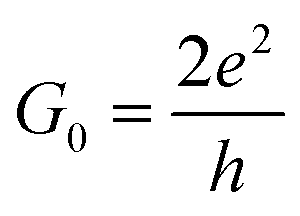 ) in sub-5 nm wide ribbons. Moreover, a simple linear relationship between the doping concentration and the ΔEF is obtained, which provides a robust means for controlling the conductivity of C5N-GNRs. Our findings are useful in understanding the effect of ordered atomic doping on the conductivity of graphene and will open up new avenues for realizing graphene-based HCMS.
Models and methods
Geometry optimizations and electronic structure calculations were performed using spin-polarized density functional theory (DFT) as implemented in Vienna Ab initio Simulation Package (VASP-5.3).46 The projector augmented wave (PAW) pseudo-potential was used to describe the core electrons, and a 500 eV cut-off energy was utilized for the valence electrons. The revised Perdew–Burke–Ernzerhof (rPBE) generalized gradient approximation (GGA)47 was chosen for the exchange correlation potential. A vacuum layer distance of 10 Å along x and y directions was used to eliminate interactions between neighboured ribbons. The k-mesh of 1 × 1 × 11 and 1 × 1 × 23 were adopted to sample the Brillouin zone (BZ) for geometry optimizations and band structure calculations. The optimization did not stop until the residual force on each atom was smaller than 0.002 eV Å−1.Electronic transport properties were examined by adopting the nonequilibrium Green’s function method in combination with density functional theory (NEGF-DFT), as implemented in SIESTA 4.2,48 by choosing double-ζ plus polarization functions (DZP) basis set for valence electrons, norm-conserving pseudopotentials for core electrons. During the calculations, a 150 Ry cut-off energy was set for real space grids, an energy shift parameter of 0.01 Ry was used to determine the cut-off radii of atomic orbitals, and a k-mesh of 1 × 1 × 100 was adopted for achieving the balance between calculated efficiency and accuracy. As an example, the constructed transport device model of the type 1–1 C5N-AGNR with width m = 2 is given in Fig. S1.†
Results and discussion
The edge structures of C5N-GNRs
Pristine GNRs have two types of edge structures.35,36 Armchair-edged GNRs (AGNRs) are nonmagnetic (NM) and can be classified into three families depending on their widths (W = 3m, 3m + 1, and 3m + 2), whereas zigzag-edged GNRs (ZGNRs) are spin-polarized with tempting antiferromagnetic (AFM) characteristics. Thus, both armchair- and zigzag-edged C5N-GNRs (C5N-AGNRs and C5N-ZGNRs) with different widths are considered in this work.We find that C5N-ZGNRs have only one kind of edge structure, while C5N-AGNRs exhibit three kinds of edge structures, which can be labelled as 1: C–C, 2: C–C′, and 3: C–N, respectively, as shown in Fig. 1. Hence, depending on the edge structures, C5N-AGNRs can be classified into six types named as 1–1, 1–2, 1–3, 2–2, 2–3, and 3–3, respectively.
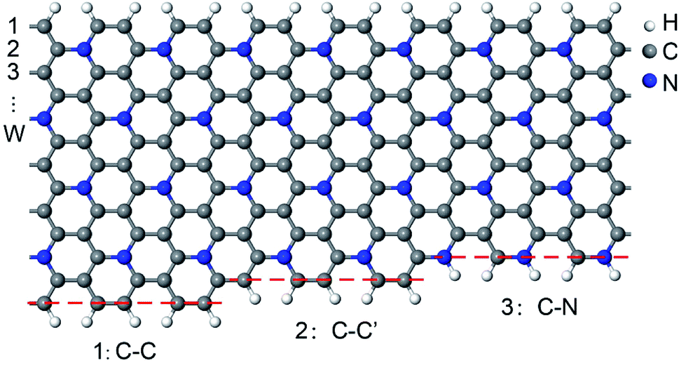 | ||
| Fig. 1 Schematic presentation of the three kinds of edge structures of C5N-AGNRs. (1) C–C, double C–C dimer lines, (2) C–C′, single C–C dimer line, and (3) C–N, single C–N dimer line. | ||
Ultrahigh conductivity in sub-5 nm wide C5N-AGNRs
We have calculated the zero-bias transmission T(E) of C5N-AGNRs at the NM state. The obtained T(E) of type 1–1 C5N-AGNRs is given in Fig. 2(a), and that of types 1–2, 1–3, 2–2, 2–3, and 3–3 are given in Fig. S3–S7,† respectively.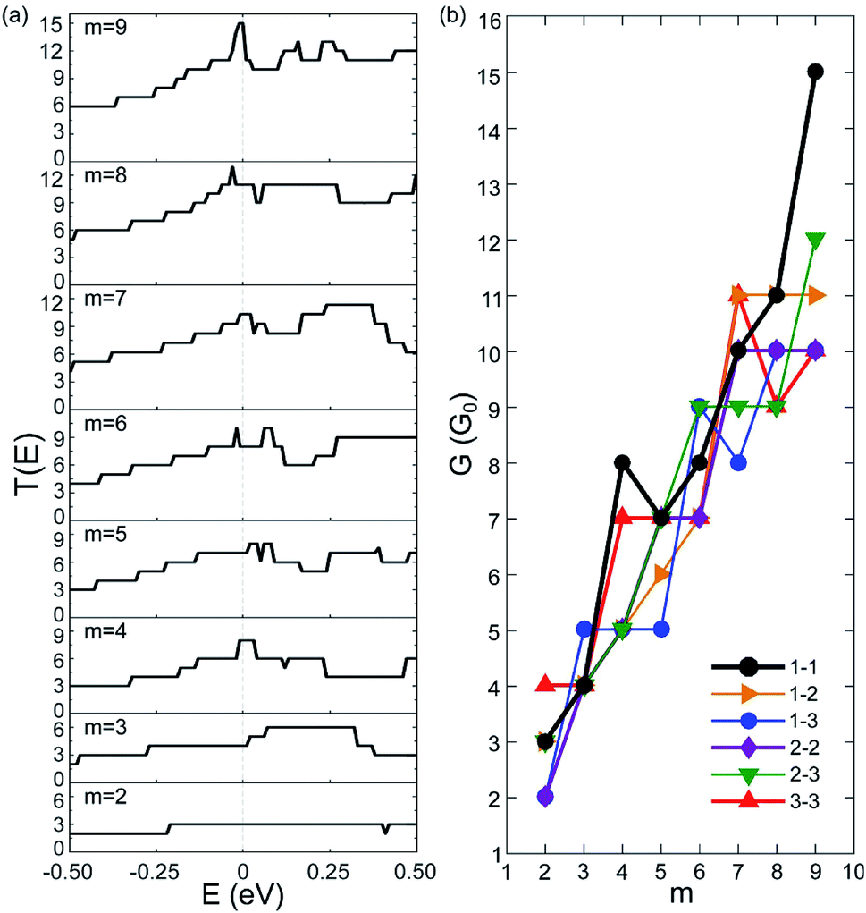 | ||
| Fig. 2 Zero-bias transmission functions (T(E)) and conductivities (G). (a) The T(E) of type 1–1 C5N-AGNRs with different widths (W), which can be represented by integers m since W = 3m + 2, (b) the calculated conductivities of all six types of C5N-AGNRs as a function of width. | ||
One can immediately see that there does not exist any transport gaps in each C5N-AGNRs, suggesting that the AGNRs are uniformly transferred from semiconducting to metallic via ordered N-doping. The intensities of T(E) are found to be integer plateaux, just as the AGNRs with fully nitrogenized edges.4 It should be noted that previous work has shown that T(E) of the GNRs with disordered N-doping exhibit non-integral intensity due to the disordered N-dopants acting as scattering centres, which reduced the transmission possibilities.25,49 Hence, the ordered N-doping does not introduce any localized states to block transport channels around the EF, or in other words the high carrier mobility of GNRs is not considerably impacted by the ordered N-doping. Moreover, one can see that the intensity of T(E) near the EF increases as the ribbon broadens, implying that wider ribbons present more conductive channels. Clearly, the orderly N-doped AGNRs exhibit much better transport capacities than the disorderly N-doped ones.
To illustrate the transport capacities, we plotted the zero-bias conductivity G of C5N-AGNRs in Fig. 2(b). One can see that each C5N-AGNR possesses an integral multiple of quantized conductivity. And as a whole, the conductivity exhibits a linear growing trend with the ribbon width. It reaches a very high value (10G0) when m = 9. Especially for type 1–1, an ultrahigh conductivity of 15G0 was achieved. Such high conductivities have never been reported in other N-doped GNRs.4,25,49,50 Considering that type 1–1 C5N-AGNRs belongs to the family of W = 3m + 2, the ribbon with m = 9 is only 3.58 nm in width, which is particularly suitable for nanoelectronics. Moreover, the linear growing trend implies that ultrahigh conductivities exist uniformly in all types of C5N-AGNRs once their widths reach the sub-5 nm level.
To gain insight into the uniformly ultrahigh conductivity, we calculated the electronic structure of the six types of C5N-AGNRs, and the result of type 1–1 is given in Fig. 3. It is evident that each ribbon is metallic with some well-delocalized partially-filled energy bands (PFEBs) crossing the EF. Meanwhile, the typical band splitting around the Dirac point of pristine AGNRs is retained, and the center of the split gap is located below the EF by ∼1 eV. It means that the EF of pristine AGNRs has been shifted up into the conduction band (CB) region by the N-doping. The number of PFEBs increased with ribbon widening. For example, the number is 3 for m = 2, and it reaches 12 for m = 9. The 12 PFEBs run across the EF 15 times in total, some of them are folded and cross the EF more than once, which directly results in the ultrahigh conductivity of 15G0 as the carrier mobility is not affected by the N-doping.
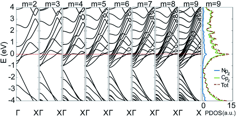 | ||
| Fig. 3 The band structures of type 1–1 C5N-AGNRs with different widths of m = 2 to 9, plus the partial density of states (PDOSs) of the ribbon with m = 9. | ||
Previous experiments have shown that N-dopants in graphene have an effective interaction force ranging up to 1.1 nm.30 The distance of neighboring N-dopants in a C5N-AGNR is only 4.26 Å, which ensures a strong interaction among N-dopants. This leads to the formation of well-delocalized PFEBs, just like the AGNRs with totally nitrogenized edges.4 Since a wider AGNR usually has more sub-bands in the conduction band (CB) region, a wider C5N-AGNR provides a higher density of states near the Fermi level, via increasing the number of PFEBs and/or enhancing the folding of PFEBs. In general, the fact that ordered N-doping induces well-delocalized PFEBs and high density of states around the Fermi level is the source of the ultrahigh conductivity in sub-5 nm wide C5N-AGNRs.
To further understand the origins of PFEBs, we have added the plot of partial density of states (PDOSs) for type 1–1 C5N-AGNR with m = 9 in Fig. 3. A sharp DOS peak with an intensity of 13 μA presents right at the EF. A previous study has shown an intensity of 3 μA in C5N-graphene,34 which is already much higher than that of graphene and GNRs. Of note, is that C5N-graphene exhibits only 2 PFEBs, but the narrow C5N-AGNR with m = 2 already has 3 PFEBs. This means that the high conductivity of C5N-graphene is inherited and carried forward in multiples in C5N-AGNRs, suggesting an advantage of C5N-AGNRs for HCMs. Moreover, it shows that the N pz orbitals distribute in a wide energy range, and the peak positions are consistent with that of the C pz orbitals. This implies that the redundant electrons of N atoms are fully integrated into the ribbon via coupling with C pz orbitals, resulting in the presence of multiple PFEBs in C5N-AGNRs. Since a well-delocalized PFEB can contribute a unit conductivity, the C5N-AGNRs of multiple well-delocalized PFEBs naturally own high conductivities.
Ultrahigh conductivity in sub-5 nm wide C5N-ZGNRs
Fig. 4(a) and (b) show the zero-bias conductivities and band structures of C5N-ZGNRs with different widths (W), respectively. One can see that the conductivities of C5N-ZGNRs also show a growing trend with width broadening, and an ultrahigh conductivity of 15G0 is also achieved for the ribbon width W = 23 (about 4.90 nm in width). It is remarkable that there exists only 2 PFEBs in the ribbon with W = 6, 7, 8, and 9, just like in the C5N-graphene, while the number of times the two PFEBs cross the EF increases from 1 to 6 as the ribbon widens, due to the shift-down of the sub-bands near the EF which leads to the enhanced folding feature of the PFEBs. Even in the wide C5N-ZGNR with W = 23, only 6 PFEBs are present, but the folding feature makes them cross the EF 15 times in total, giving rise to the high conductivity. Hence, it is safe to say that ultrahigh conductivity is also achievable in sub-5 nm wide C5N-ZGNRs.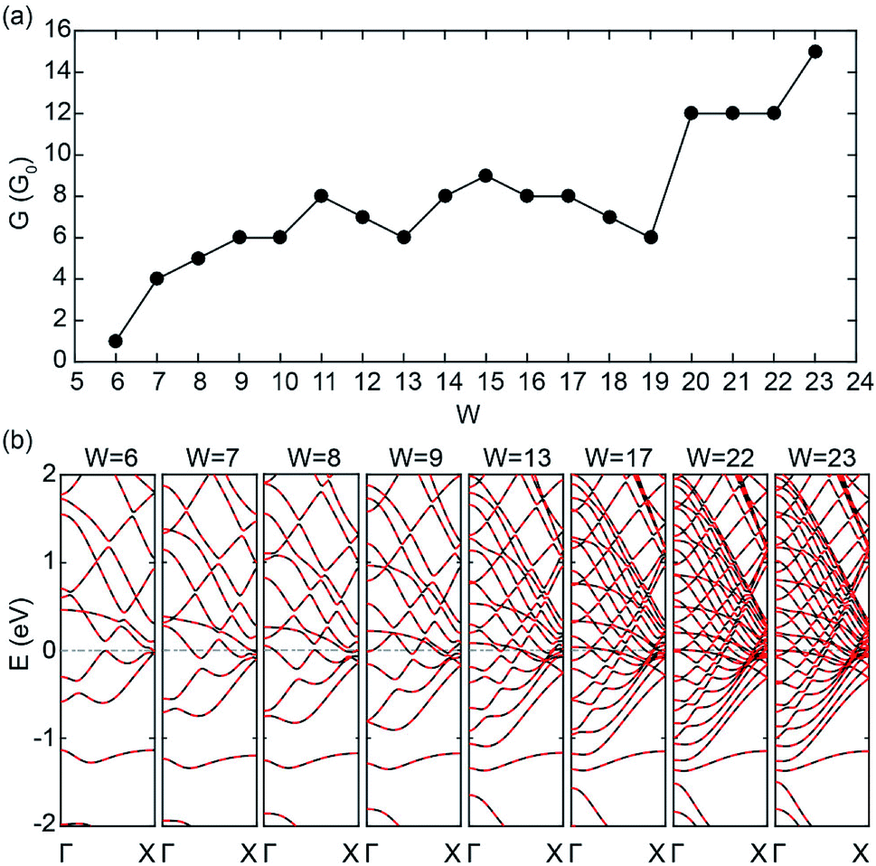 | ||
| Fig. 4 (a) Zero-bias conductivities and (b) band structure of C5N-ZGNRs with different widths (W) at the AFM ground state. | ||
Linear relationship between ΔEF and doping concentration
We have plotted ΔEF (ΔEF ≡ EF(C5N-GNR) − EF(GNR)) as the function of the doping concentration (c) for all considered GNRs in Fig. 5. From the inset, one can see that the type 1–3 and type 2–2 C5N-AGNRs and the C5N-ZGNRs possess a constant doping concentration of 16.7%, just as in the C5N-graphene. While in the other four types of C5N-AGNR, the doping concentration either increases or decreases exponentially with increasing width, and can ultimately converge to the value of 16.7%.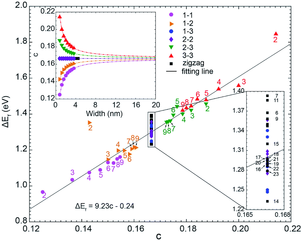 | ||
| Fig. 5 The scatter plot of the shift of Fermi level (ΔEF) as a function of doping concentration (c). Inset shows the relationship between doping concentration (c) and the ribbon width. | ||
Overall, a simple relationship between ΔEF and doping concentration (c) can be seen, which can be described by a linear fitting of ΔEF = 9.23c − 0.24. It shows that the doping concentration plays a decisive role in determining the ΔEF. Significant deviations appear only for narrow ribbons, especially for the ribbons with m = 2, due to strong quantum confinement which only exists in narrow ribbons.
Conclusions
In conclusion, we have systematically studied the electronic structure and electron conductivity of orderly nitrogen-doped graphene nanoribbons (C5N-GNRs) from first principles calculations. By carefully evaluating the edge type (armchair and zigzag), edge structure (single C–N, single C–C, and double C–C), ribbon width, doping concentration, and quantum confinement effect, a simple linear relationship between the shift-up of the Fermi level and the doping concentration is obtained. It is found that the ordered N-doping increases the carrier density by shifting the Fermi level to the CB region but does not considerably impact the high carrier mobility of the system due to the nonexistence of localized states near the Fermi level. Hence, ultrahigh conductivities (>15G0) can be achieved in sub-5-nanometer-wide C5N-GNRs, which calls for an increased effort in using ordered atomic doping for band structure engineering of carbon nanomaterials to utilize high conductivity materials at the nanoscale.In light of recent developments, one can believe that the synthesis of our proposed C5N-GNRs is feasible. As an example, Cui, et al.34 has proposed a kinetic pathway toward C5N-graphene on Cu(111) using C5NCl5 precursors. Chen et al.43 have found that oriented GNRs can grow in hexagonal boron nitride (h-BN) trenches. Moreover, the GNR with ordered N-doping at the edges is achievable via bottom-up techniques. Once C5N-graphene is realized in experiments, C5N-GNRs can also be obtained from C5N-graphene via modern lithographically patterned technologies, such as producing GNRs from graphene sheets.
Conflicts of interest
There are no conflicts to declare.Acknowledgements
This work was supported by the National Key Research and Development Program of China (2017YFA0303500), National Natural Science Foundation of China (21643011, 61701175, 21633007, 21790350), Hunan Provincial Natural Science Foundation of China (Grant No. 27JJ3050), the Fundamental Research Foundations for the Central Universities, Sichuan Provincial Postdoctoral Science Foundation of China, and Anhui Initiative in Quantum Information Technologies.Notes and references
- L. Lu, Y. Shen, X. Chen, L. Qian and K. Lu, Science, 2004, 304, 422–426 CrossRef CAS PubMed.
- Y. Liang, X. Liang, Z. Zhang, W. Li, X. Huo and L. Peng, Nanoscale, 2015, 7, 10954–10962 RSC.
- T. M. Higgins and J. N. Coleman, ACS Appl. Mater. Interfaces, 2015, 7, 16495–16506 CrossRef CAS PubMed.
- L. Liu, X.-F. Li, Q. Yan, Q.-K. Li, X.-H. Zhang, M. Deng, Q. Qiu and Y. Luo, Phys. Chem. Chem. Phys., 2017, 19, 44–48 RSC.
- M. Park, J. Im, M. Shin, Y. Min, J. Park, H. Cho, S. Park, M.-B. Shim, S. Jeon, D.-Y. Chung, J. Bae, J. Park, U. Jeong and K. Kim, Nat. Nanotechnol., 2012, 7, 803 CrossRef CAS PubMed.
- N. Matsuhisa, M. Kaltenbrunner, T. Yokota, H. Jinno, K. Kuribara, T. Sekitani and T. Someya, Nat. Commun., 2015, 6, 7461 CrossRef CAS PubMed.
- F. Hoeng, A. Denneulin and J. Bras, Nanoscale, 2016, 8, 13131–13154 RSC.
- H. Kim, D.-H. Seo, S.-W. Kim, J. Kim and K. Kang, Carbon, 2011, 49, 326–332 CrossRef CAS.
- J.-H. Choi, H. Wang, S. J. Oh, T. Paik, P. Sung, J. Sung, X. Ye, T. Zhao, B. T. Diroll, C. B. Murray and C. R. Kagan, Science, 2016, 352, 205–208 CrossRef CAS PubMed.
- S. Jung, S. J. Chun, J. T. Han, J. S. Woo, C.-H. Shon and G.-W. Lee, Nanoscale, 2016, 8, 5343–5349 RSC.
- C. Zhang, Z. Ni, J. Zhang, X. Yuan, Y. Liu, Y. Zou, Z. Liao, Y. Du, A. Narayan, H. Zhang, T. Gu, X. Zhu, L. Pi, S. Sanvito, X. Han, J. Zou, Y. Shi, X. Wan, S. Y. Savrasov and F. Xiu, Nat. Mater., 2019, 18, 482 CrossRef CAS PubMed.
- F. Xu and Y. Zhu, Adv. Mater., 2012, 24, 5117–5122 CrossRef CAS PubMed.
- X. Huang, P. Sheng, Z. Tu, F. Zhang, J. Wang, H. Geng, Y. Zou, C.-a. Di, Y. Yi, Y. Sun, W. Xu and D. Zhu, Nat. Commun., 2015, 6, 7408 CrossRef CAS PubMed.
- Z. Li, G. Ma, R. Ge, F. Qin, X. Dong, W. Meng, T. Liu, J. Tong, F. Jiang and Y. Zhou, Angew. Chem., Int. Ed., 2016, 55, 979–982 CrossRef CAS PubMed.
- Y. Ding, J. Zhang, L. Chang, X. Zhang, H. Liu and L. Jiang, Adv. Mater., 2017, 29, 1704253 CrossRef PubMed.
- Z. Deng, Y. Guo, X. Zhao, P. X. Ma and B. Guo, Chem. Mater., 2018, 30, 1729–1742 CrossRef CAS.
- T. N. Tu, N. Q. Phan, T. T. Vu, H. L. Nguyen, K. E. Cordova and H. Furukawa, J. Mater. Chem. A, 2016, 4, 3638–3641 RSC.
- D. Sheberla, L. Sun, M. A. Blood-Forsythe, S. Er, C. R. Wade, C. K. Brozek, A. Aspuru-Guzik and M. Dincă, J. Am. Chem. Soc., 2014, 136, 8859–8862 CrossRef CAS PubMed.
- Y. Chang, A. D. Mohanty, S. B. Smedley, K. Abu-Hakmeh, Y. H. Lee, J. E. Morgan, M. A. Hickner, S. S. Jang, C. Y. Ryu and C. Bae, Macromolecules, 2015, 48, 7117–7126 CrossRef CAS.
- G. Manthilake, N. Bolfan-Casanova, D. Novella, M. Mookherjee and D. Andrault, Sci. Adv., 2016, 2, e1501631 CrossRef PubMed.
- A. K. Geim, Science, 2009, 324, 1530–1534 CrossRef CAS PubMed.
- L. Zhang, F. Zhang, X. Yang, G. Long, Y. Wu, T. Zhang, K. Leng, Y. Huang, Y. Ma, A. Yu and Y. Chen, Sci. Rep., 2013, 3, 1408 CrossRef PubMed.
- M. A. Worsley, P. J. Pauzauskie, T. Y. Olson, J. Biener, J. H. Satcher Jr and T. F. Baumann, J. Am. Chem. Soc., 2010, 132, 14067–14069 CrossRef CAS PubMed.
- M. Lin, Y. Gai, D. Xiao, H. Tan and Y. Zhao, Chem. Phys. Lett., 2018, 713, 98–104 CrossRef CAS.
- B. Biel, X. Blase, F. Triozon and S. Roche, Phys. Rev. Lett., 2009, 102, 096803 CrossRef PubMed.
- X. Wang, G. Sun, P. Routh, D.-H. Kim, W. Huang and P. Chen, Chem. Soc. Rev., 2014, 43, 7067–7098 RSC.
- W.-W. Yan, X.-F. Li, X.-H. Zhang, X. Cao and M. Deng, J. Mater. Chem. C, 2019, 7, 6241–6245 RSC.
- X. Wang, X. Li, L. Zhang, Y. Yoon, P. K. Weber, H. Wang, J. Guo and H. Dai, Science, 2009, 324, 768–771 CrossRef CAS PubMed.
- Y. Wang, Y. Shao, D. W. Matson, J. Li and Y. Lin, ACS Nano, 2010, 4, 1790–1798 CrossRef CAS PubMed.
- R. Lv, Q. Li, A. R. Botello-Mendez, T. Hayashi, B. Wang, A. Berkdemir, Q. Hao, A. L. Elias, R. Cruz-Silva, H. R. Gutierrez, Y. A. Kim, H. Muramatsu, J. Zhu, M. Endo, H. Terrones, J.-C. Charlier, M. Pan and M. Terrones, Sci. Rep., 2012, 2, 586 CrossRef PubMed.
- X.-F. Li, Q.-K. Li, J. Cheng, L. Liu, Q. Yan, Y. Wu, X.-H. Zhang, Z.-Y. Wang, Q. Qiu and Y. Luo, J. Am. Chem. Soc., 2016, 138, 8706–8709 CrossRef CAS PubMed.
- Q.-K. Li, X.-F. Li, G. Zhang and J. Jiang, J. Am. Chem. Soc., 2018, 140, 15149–15152 CrossRef CAS PubMed.
- T. Schiros, D. Nordlund, L. Palova, D. Prezzi, L. Zhao, K. S. Kim, U. Wurstbauer, C. Gutierrez, D. Delongchamp and C. Jaye, Nano Lett., 2012, 12, 4025–4031 CrossRef CAS PubMed.
- P. Cui, J.-H. Choi, C. Zeng, Z. Li, J. Yang and Z. Zhang, J. Am. Chem. Soc., 2017, 139, 7196–7202 CrossRef CAS.
- M. Y. Han, B. Özyilmaz, Y. Zhang and P. Kim, Phys. Rev. Lett., 2007, 98, 206805 CrossRef PubMed.
- Y.-W. Son, M. L. Cohen and S. G. Louie, Phys. Rev. Lett., 2006, 97, 216803 CrossRef.
- X. Wang, Y. Ouyang, X. Li, H. Wang, J. Guo and H. Dai, Phys. Rev. Lett., 2008, 100, 206803 CrossRef.
- J. Cai, C. A. Pignedoli, L. Talirz, P. Ruffieux, H. Söde, L. Liang, V. Meunier, R. Berger, R. Li, X. Feng, K. Mullen and R. Fasel, Nat. Nanotechnol., 2014, 9, 896–900 CrossRef CAS PubMed.
- N. Richter, Z. Chen, A. Tries, T. Prechtl, A. Narita, K. Müllen, K. Asadi, M. Bonn and M. Kläui, arXiv preprint arXiv:1806.00962, 2018.
- P. Ruffieux, S. Wang, B. Yang, C. Sánchez-Sánchez, J. Liu, T. Dienel, L. Talirz, P. Shinde, C. A. Pignedoli, D. Passerone, T. Dumslaff, X. Feng, K. Mullen and R. Fasel, Nature, 2016, 531, 489–492 CrossRef CAS PubMed.
- A. Narita, X. Feng, Y. Hernandez, S. A. Jensen, M. Bonn, H. Yang, I. A. Verzhbitskiy, C. Casiraghi, M. R. Hansen, A. H. Koch, G. Fytas, O. Ivasenko, B. Li, K. S. Mali, T. Balandina, S. Mahesh, S. D. Feyter and K. Mullen, Nat. Chem., 2014, 6, 126 CrossRef CAS PubMed.
- C. Ma, Z. Xiao, H. Zhang, L. Liang, J. Huang, W. Lu, B. G. Sumpter, K. Hong, J. Bernholc and A.-P. Li, Nat. Commun., 2017, 8, 14815 CrossRef CAS PubMed.
- L. Chen, L. He, H. S. Wang, H. Wang, S. Tang, C. Cong, H. Xie, L. Li, H. Xia and T. Li, et al. , Nat. Commun., 2017, 8, 14703 CrossRef PubMed.
- Z. Chen, H. I. Wang, J. Teyssandier, K. S. Mali, T. Dumslaff, I. Ivanov, W. Zhang, P. Ruffieux, R. Fasel, H. J. Rader, D. Turchinovich, S. D. Feyter, X. Feng, M. Klaui, A. Narita, M. Bonn and K. Mullen, J. Am. Chem. Soc., 2017, 139, 3635–3638 CrossRef CAS PubMed.
- I.-Y. Jeon, H.-J. Choi, M. J. Ju, I. T. Choi, K. Lim, J. Ko, H. K. Kim, J. C. Kim, J.-J. Lee, D. Shin, S.-M. Jung, J.-M. Seo, M.-J. Kim, N. Park, L. Dai and J.-B. Baek, Sci. Rep., 2013, 3, 2260 CrossRef PubMed.
- G. Kresse and J. Furthmüller, Phys. Rev. B: Condens. Matter Mater. Phys., 1996, 54, 11169 CrossRef CAS PubMed.
- J. P. Perdew, K. Burke and M. Ernzerhof, Phys. Rev. Lett., 1996, 77, 3865 CrossRef CAS PubMed.
- J. M. Soler, E. Artacho, J. D. Gale, A. García, J. Junquera, P. Ordejón and D. Sánchez-Portal, J. Phys.: Condens. Matter, 2002, 14, 2745 CrossRef CAS.
- H. Ren, Q.-X. Li, Y. Luo and J. Yang, Appl. Phys. Lett., 2009, 94, 173110 CrossRef.
- X.-F. Li, K.-Y. Lian, Q. Qiu and Y. Luo, Nanoscale, 2015, 7, 4156–4162 RSC.
Footnote |
| † Electronic supplementary information (ESI) available: Fig. S1–S7. See DOI: 10.1039/c9na00458k |
| This journal is © The Royal Society of Chemistry 2019 |