
 Open Access Article
 This Open Access Article is licensed under a
 Creative Commons Attribution 3.0 Unported Licence
Tailoring the crystal growth of quartz on silicon for patterning epitaxial piezoelectric films†
Qianzhe
Zhang
ab,
David
Sánchez-Fuentes
b,
Andrés
Gómez
 a,
Rudy
Desgarceaux
b,
Benoit
Charlot
b,
Jaume
Gàzquez
a,
Adrián
Carretero-Genevrier
*b and
Martí
Gich
*a
a,
Rudy
Desgarceaux
b,
Benoit
Charlot
b,
Jaume
Gàzquez
a,
Adrián
Carretero-Genevrier
*b and
Martí
Gich
*a
aInstitut de Ciència de Materials de Barcelona (ICMAB), Consejo Superior de Investigaciones Científicas (CSIC), Campus UAB, 08193 Bellaterra, Catalonia, Spain. E-mail: marti.gich@csic.es
bInstitut d'Électronique et des Systèmes (IES), UMR 5214, CNRS, Université de Montpellier, 860 rue Saint Priest, 34095 Montpellier, France. E-mail: carretero@ies.univ-montp2.fr
First published on 29th August 2019
Abstract
Epitaxial films of piezoelectric α-quartz could enable the fabrication of sensors with unprecedented sensitivity for prospective applications in electronics, biology and medicine. However, the prerequisites are harnessing the crystallization of epitaxial α-quartz and tailoring suitable film microstructures for nanostructuration. Here, we bring new insights into the crystallization of epitaxial α-quartz films on silicon (100) from the devitrification of porous silica and the control of the film microstructures: we show that by increasing the quantity of devitrifying agent (Sr) it is possible to switch from an α-quartz microstructure consisting of a porous flat film to one dominated by larger, fully dense α-quartz crystals. We also found that the film thickness, relative humidity and the nature of the surfactant play an important role in the control of the microstructure and homogeneity of the films. Via a multi-layer deposition method, we have extended the maximum thickness of the α-quartz films from a few hundreds of nm to the μm range. Moreover, we found a convenient method to combine this multilayer approach with soft lithography to pattern silica films while preserving epitaxial crystallization. This improved control over crystallization and the possibility of preparing patterned films of epitaxial α-quartz on Si substrates pave the path to future developments in applications based on electromechanics, optics and optomechanics.
1. Introduction
Silicon and oxygen are the most abundant elements in the earth's crust. Accordingly, silica (SiO2), in the form of [SiO4] tetrahedral networks, is a basic building block of most minerals. For centuries, those minerals have been massively exploited for the production of building materials such as glass or concrete, but more recently silicates have found a wide range of high-end applications, from the use of zeolites in catalysis to the incorporation of lutetium silicates in scintillators.1 Quartz single crystals are a remarkable example of such high technology applications of minerals. Thanks to their piezoelectric properties with a high resonance quality factor, thin quartz plates are used as electric oscillators providing a stable clock frequency in virtually any electronic appliance. Since the resonant frequency of the plates is extremely sensitive to their mass and thickness, quartz crystals are also exploited in microgravimetric devices for sensing applications.2,3 Moreover, thanks to their non-centrosymmetric and chiral structure, quartz crystals present optical activity, finding applications in optics.4Fully exploiting the potential of quartz and other functional silicates in current and future applications requires controlling their microstructure down to the nanoscale. Yet, despite the importance of silicates in leading edge applications, fundamental aspects of their crystallisation are still poorly understood. A paradigmatic example of this is the highly empirical and poorly predictive devitrification of amorphous silicates. Indeed, even controlling the crystallization of SiO2 is a long-standing problem related to the remarkable stability of silica and the tiny differences in free energies of formation between all its amorphous and crystalline forms.5
Lately, fundamental and application-driven interest in nanoscale SiO2 provided new insights towards understanding and controlling silica devitrification in microporous, mesoporous and ultrathin silica.6–15 Most of these studies highlight the essential role of alkaline,11 alkaline earth8–10,15 and transition metal dopants7 in obtaining the desired crystallization. For instance, the formation of iron silicate seeds underpins the epitaxial growth of thermally evaporated ultrathin silica on Ru (0001).13 Other studies show that, at the nanoscale, the confinement of alkaline or alkaline earth melting agents is essential for achieving a controlled crystallization of α-quartz. In particular, we prepared superlattices of polycrystalline α-quartz nanospheres by impregnating preformed 3D stackings of mesoporous silica spheres with aqueous solutions of alkaline earth cations followed by thermal treatments above 800 °C. However, using a Li3+ solution we observed a straightforward crystallization of α-quartz and lithium silicate with a loss of the superstructure morphology, at temperatures as low as 650 °C. In contrast, Matsuno et al.11 obtained α-quartz nanosphere superlattices with improved crystallinity at 870 °C after confining Li+ between silica spheres and a reinforcing carbon coating. Ndayishimiye et al.12 impregnated microporous SiO2 nanoparticles with NaOH solutions and studied their hydrothermal sintering, finding an amorphous product below a concentration threshold (1 M) while dense polycrystalline α-quartz resulted from impregnations with more concentrated solutions.12
Also, the use of surfactants in the synthesis of mesoporous silica can strongly influence the devitrification. For instance, with the presence of amphiphiles the temperature of silica crystallization under high pressure was lower than in the case where the surfactants had been previously removed.14 In this sense, Putz et al. used sodium metasilicate solutions in microemulsions to obtain small α-quartz nanocrystals at room temperature or under mild hydrothermal conditions below 200 °C.15 The above examples illustrate the complexity of controlling the crystallization and microstructure of nanostructured α-quartz and highlight the critical roles of the silica porosity, the concentration, distribution and confinement of devitrifying agents or the presence of surfactants.
We recently developed a chemical solution deposition method for preparing epitaxial α-quartz films on Si (100) substrates. The method relies on the thermal devitrification of dip-coated mesoporous silica films, assisted by alkaline earth cations in amphiphilic molecular templates.8 By varying the surfactants and the synthesis conditions the porosity of the mesoporous silica can be tailored to range from a few tens of nm to 1 μm and is preserved upon crystallization. But pore sizes below 40 nm cannot be retained in the crystalline replica: the films display rough surfaces of densely packed crystals with lateral sizes below 500 nm coexisting with significantly larger single crystalline domains attaining several tens of μm. Such single crystalline domains of fully dense α-quartz can be appealing for fabricating nanostructured optical metamaterials and devices,16 minimizing the scattering losses. In contrast, for microgravimetric sensors, it would be advantageous to have films with low roughness (enabling the fabrication of surface acoustic wave devices by lithography) and some degree of porosity (to achieve an increased mass sensitivity).
A prerequisite to enable these technological applications is gaining a greater control over the crystallization of epitaxial quartz. On the one hand, a method to prepare porous films displaying low roughness has not been reported so far. On the other hand, the synthesis of large single crystalline dense α-quartz follows a quite inconvenient 2-step process.8 This involves the impregnation of a preformed silica film in a solution of the devitrifying agent, and the need for cleaning the film surface from an excess of impregnating solution entails irreproducibility issues. Moreover, most applications require controlling the film thickness from hundreds of nm to above 1 μm, but the maximum thicknesses of epitaxial quartz films prepared by the dip coating technique do not exceed a few hundred nm.
To address these shortcomings our aim was to control the microstructure of epitaxial α-quartz films on silicon. We focused on understanding the roles of the concentration of the devitrifying agent (Sr2+), the relative humidity and the film roughness and thickness, which has been poorly studied so far. These proved to be crucial for tailoring the film microstructure and implementing a procedure to increase the film thickness up to the micron range. We exploited this enhanced control over the crystallization to prepare high-quality patterns of epitaxial quartz films by soft lithography.
2. Experimental
2.1 Synthesis
![[thin space (1/6-em)]](https://www.rsc.org/images/entities/char_2009.gif) :Brij-58:HCl:EtOH:SrCl2 = 1:0.3:0.7:25:0.05 having a Sr/SiO2 molar ratio of 0.05. For samples with other Sr contents, the molar ratio of SrCl2 with respect to TEOS is given by 0.05 times the corresponding molarity of Solution B. Taking this into account the SrCl2/TEOS molar ratios studied in this work (and the corresponding Sr/SiO2 molar ratios of the quartz films) range from 0.02 to 0.1 (see Table S1†). Thus, hereafter the Sr content of the different quartz films is expressed by the Sr/SiO2 molar ratios, labeled RSr. To explore the effect of different types of surfactants we prepared films in which the oligomeric alkyl poly(ethylene oxide) Brij-58 was replaced by alternative surfactants such as the ionic cetyltrimethylammonium bromide (CTAB) and the poly(ethylene oxide) triblock copolymer Pluronic F127, with the following reference compositions for Solution C TEOS:CTAB:HCl:EtOH:SrCl2 = 1:0.14:0.7:25:0.05 and TEOS:F127:HCl:EtOH:SrCl2 = 1:0.0055:0.7:25:0.05.
:Brij-58:HCl:EtOH:SrCl2 = 1:0.3:0.7:25:0.05 having a Sr/SiO2 molar ratio of 0.05. For samples with other Sr contents, the molar ratio of SrCl2 with respect to TEOS is given by 0.05 times the corresponding molarity of Solution B. Taking this into account the SrCl2/TEOS molar ratios studied in this work (and the corresponding Sr/SiO2 molar ratios of the quartz films) range from 0.02 to 0.1 (see Table S1†). Thus, hereafter the Sr content of the different quartz films is expressed by the Sr/SiO2 molar ratios, labeled RSr. To explore the effect of different types of surfactants we prepared films in which the oligomeric alkyl poly(ethylene oxide) Brij-58 was replaced by alternative surfactants such as the ionic cetyltrimethylammonium bromide (CTAB) and the poly(ethylene oxide) triblock copolymer Pluronic F127, with the following reference compositions for Solution C TEOS:CTAB:HCl:EtOH:SrCl2 = 1:0.14:0.7:25:0.05 and TEOS:F127:HCl:EtOH:SrCl2 = 1:0.0055:0.7:25:0.05.
2.2 Nanostructuration process
2.3 Structural characterization and piezoelectric measurements
3. Results and discussion
3.1 Influence of the Sr content in the microstructure of epitaxial quartz
We performed a systematic study on the influence of Sr content in the microstructure, crystallinity and epitaxial growth quality of quartz films obtained following the same annealing treatment at 1000 °C. For this, we prepared porous silica films under identical deposition conditions (see Gel films by dip coating in Section 2.1) with Sr/SiO2 molar ratios (RSr) between 0 and 0.1. Fig. 1 shows the evolution of the characteristic microstructures of the film surfaces upon increasing the Sr content as observed from AFM topography images (Fig. 1a) and SEM in backscattered electron mode (Fig. 1b).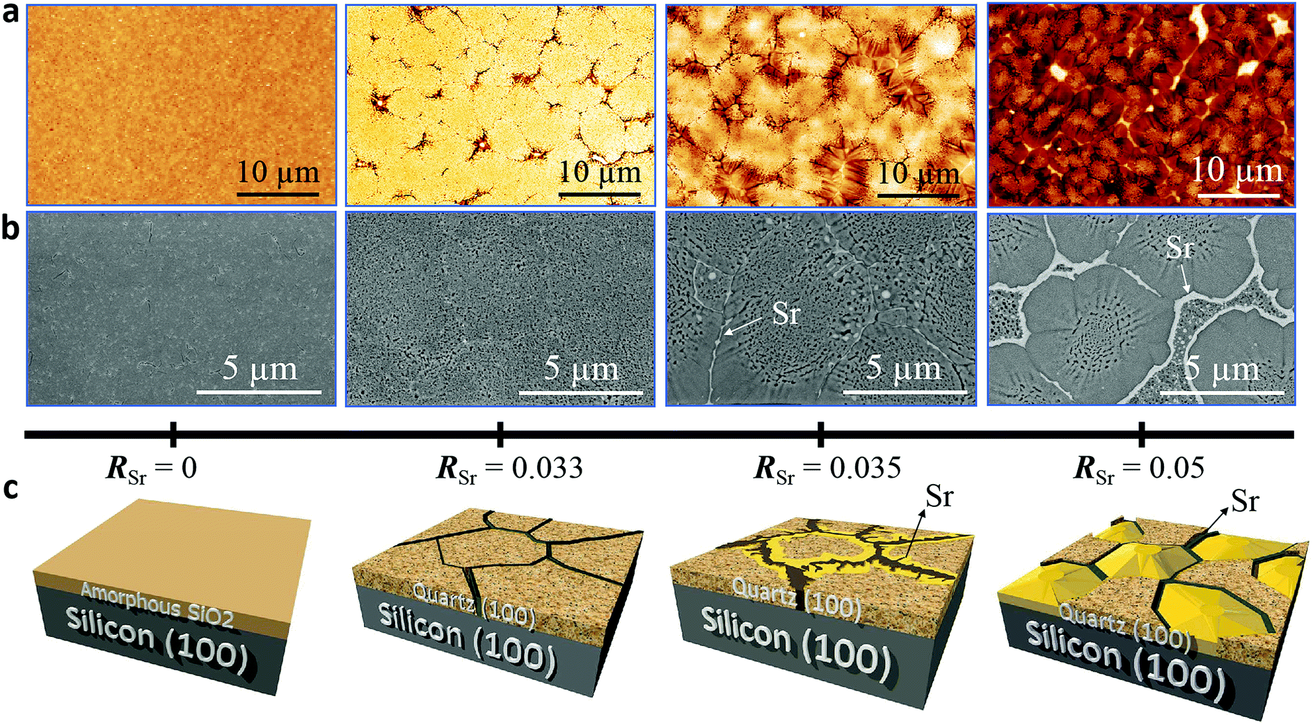 | ||
| Fig. 1 The microstructures of α-quartz films containing different amounts of Sr (0 < RSr < 0.05 indicated in a scale below the images) are revealed by AFM (a) and SEM in backscattered electron mode (b). The salient features of these microstructures are illustrated in the 3D model (c). Those films were prepared with a withdrawal speed of 5 mm s−1 under a relative humidity of 40% at 25 °C using Brij-58 as the surfactant. The annealing treatment was at 1000 °C for 300 minutes in an air atmosphere. | ||
Fig. 1c provides a sketch emphasizing the salient features of the microstructural changes induced by increasing the Sr content, which we describe below. The films without Sr, (leftmost images in Fig. 1a and b), are characterized by their homogeneity with some cracks and sparse pores (see Fig. S1†). In contrast, the Sr-containing films present crevices which define roughly elliptical domains of sizes between 5 and 10 μm in an arrangement reminiscent of mud-cracking patterns, but with the presence within the domains of many pores of sizes below 300 nm. Notice that for the films with RSr > 0.033 (two rightmost images in Fig. 1a and b), in the areas bordering the domain boundaries, the porosity has given way to fully dense faceted structures which are characteristic of crystals. These dense structures (the yellow zone in Fig. 1c) become more prominent as RSr increases and prevail for RSr = 0.05, leaving only a residual porous zone at the center of the domains. The SEM images (Fig. 1b) show that these dense structures are accompanied by bright white contrasts at the domain boundaries which were ascribed to accumulations of Sr, the presence of which was confirmed by XPS (see Fig. S2†). Note that these Sr-rich areas present irregular and droplet-like shapes in the regions with porous microstructures, suggesting that these have been a liquid phase at the annealing temperature. However, at some point during the cooling the Sr-rich phase undergoes a process of carbonation and SrCO3 is its major component at room temperature, as we previously reported.9 The AFM images of the films with dense structures (see Fig. 1a) present a more rugged topography. This is reflected in the fivefold increase of the root mean square roughness (from 5 nm to 25 nm) for RSr increasing from 0.033 to 0.1 (see Fig. S3†).
We investigated the characteristic microstructure of the films with RSr = 0.033 (porous) and RSr = 0.05 (dense domains) by scanning transmission electron microscopy (STEM). Fig. 2b and e present Z-contrast low magnification images of the quartz films from the zones indicated by red-dotted lines in the 3D sketches, which represent the salient characteristics of the porous and dense films (Fig. 2a and d, respectively). Fig. 2b shows interconnected pores with diameters in the range of 50–100 nm. Distributed within the pores there are small whitish features of about 10–20 nm which correspond to Sr agglomerates. An analogous microstructure is observed on the left-hand side of Fig. 2e, next to a large Sr aggregate which marks the transition to a thinner dense structure on the right-hand side of the image. The atomic resolution images of Fig. 2c and f and the corresponding fast Fourier transform (FFT) patterns (shown in the insets) indicate that both the porous and dense structures are α-quartz crystals with well-defined orientations. In particular, the FFTs of Fig. 2c, which correspond to the orientation of the Si substrate and α-quartz crystals along their [100] zone axes, are indicative of an epitaxial growth with Si (100)//α-quartz (100) and Si (010)//α-quartz (010), in agreement with our previous report.8 Such epitaxial relationships have been confirmed both for porous and dense quartz films by X-ray diffraction, with θ–2θ scans (Fig. 3a) and pole figures of the Si {111} and α-quartz {101} reflections (see Fig. S4†).
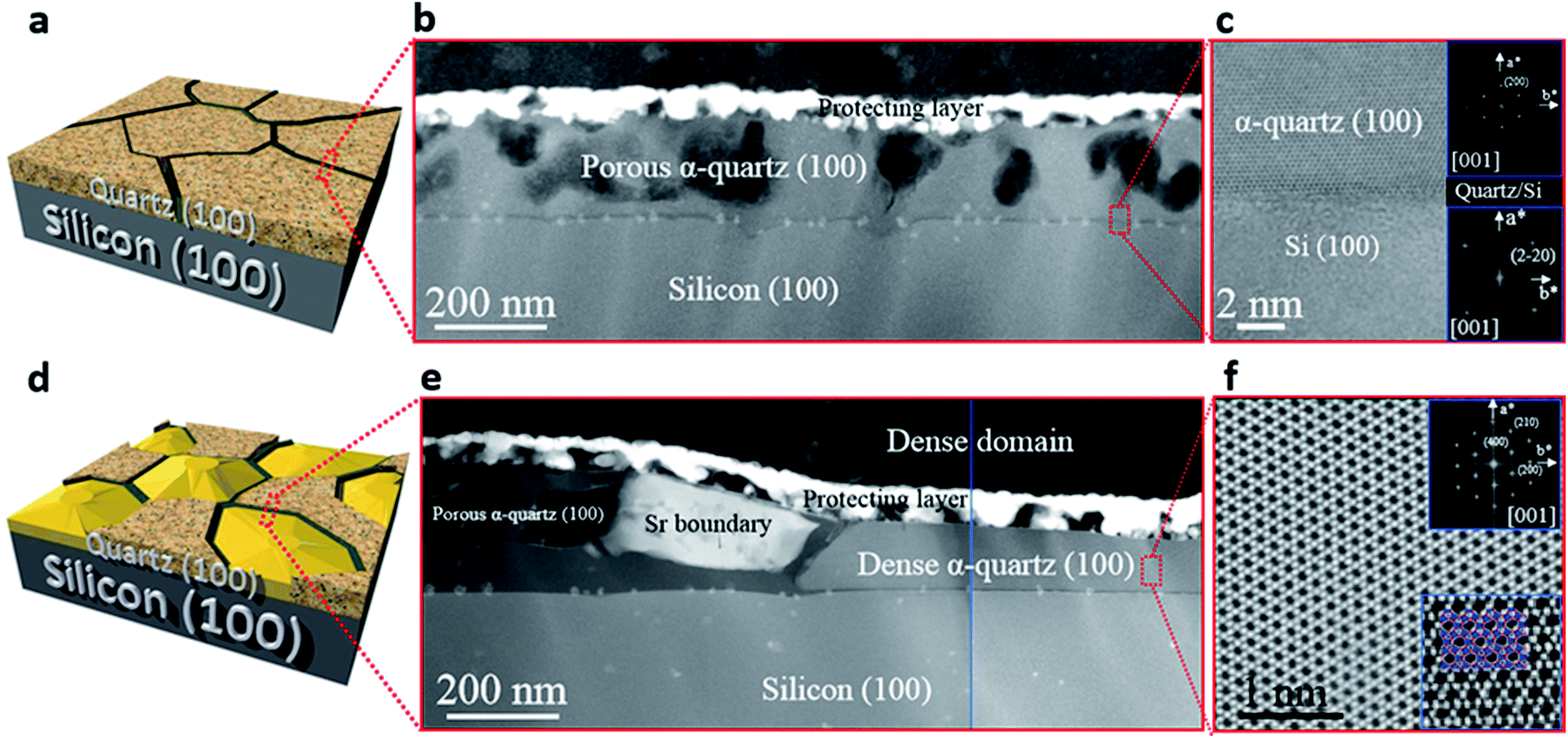 | ||
| Fig. 2 Cross-sectional STEM images: (a) and (d) are the 3D representations for two different microstructures with the red dotted lines indicating the cross-sections to which the images correspond. (b) Low magnification Z-contrast image of the porous film (RSr = 0.033). (c) Bright field STEM atomic resolution image of the porous film cross-section showing the interface between the α-quartz (100) film and silicon (100) substrate. The insets are the FFT patterns of the film and substrate, respectively. (e) Low magnification Z-contrast image of the dense film (RSr = 0.05). (f) Bright field STEM atomic resolution image of the dense film cross-section. The upper inset is the FFT pattern and the lower inset a higher magnification image displaying the model structure with the tetrahedral Si in blue, surrounded by oxygens in red. | ||
 | ||
| Fig. 3 (a) XRD θ–2θ scan results of films with different RSr. (b) Relationship between the FWHM of rocking curves of α-quartz (100) and RSr. (c) Influence of RSr on the area coverage of dense α-quartz. Those films were prepared with a withdrawal speed of 5 mm s−1 under a relative humidity of 40% at 25 °C using Brij-58 as the surfactant. The annealing treatment was at 1000 °C for 300 minutes in an air atmosphere. | ||
Fig. 3a shows that the intensities of the (100) and (200) reflections of α-quartz increase with RSr. In particular, the film with RSr = 0.02 does not present any diffraction peak. However, by observing this film with an optical microscope we noticed the presence of some crystals (see Fig. S5a–c†), which were not found in films with lower RSr. The optical microscopy observations also suggested the presence of a residual amorphous phase for films with 0.02 < RSr < 0.033 which was confirmed by electron backscatter diffraction (EBSD) observations for the film with RSr = 0.02 (see Fig. S5d–f†). For RSr = 0.033 the film is fully crystallized and presents the characteristic porosity that we described above, which is not observed for amorphous or poorly crystallized films. This porosity originates from the larger density of α-quartz (2.65 g cm−3) compared to that of amorphous SiO2 (2.20 g cm−3)22 with the resulting need to accommodate the volume shrinkage upon crystallization. The densification of SiO2 is also responsible for the formation of domains delimited by cracks which, as we shall discuss below, play an important role in the formation of dense crystal structures. The inset of Fig. 3b presents a series of θ–ω measurements of the (100) α-quartz reflection (rocking curves) for films with different Sr contents, showing that their full widths at half maximum (FWHM) are lowered by increasing RSr. The FWHM decreases steeply when RSr rises from 0.025 up to 0.035 but much more slowly and tending to level off for higher Sr concentrations. This indicates that the effect of RSr on the misorientation of α-quartz crystals follows two differentiated regimes delimited by RSr between 0.033 and 0.035. This coincides with the threshold concentration range above which dense films can be stabilized over the porous morphologies, as is evidenced in the plot of surface coverage by dense crystals vs. RSr (Fig. 3b). An equivalent sharp transition is observed at similar Sr contents in the evolution of film roughness vs. RSr as shown in Fig. S3.† It is quite remarkable that the crystallization of films with porous morphology (RSr = 0.033) does not generate a marked increase in the surface roughness as occurs for the crystallization of films with dense morphologies (RSr = 0.05). Indeed, for porous films the roughness can be as low as 4.6 nm, only slightly above that of an amorphous film before crystallization (4 nm). The larger mosaicity of porous films results from slight misorientations of different crystals as they nucleate on the substrate wherever there is enough Sr to allow the devitrification. However, their growth is limited by the availability of Sr which forms small size aggregates. Hence, the different crystals join forming low energy domain boundaries and the film planarity is maintained through the porosity that accommodates the volume collapse. When SiO2 crystallizes, Sr is expulsed into the empty spaces that have been created, forming larger aggregates. The accretion of Sr becomes more important as RSr increases and, for RSr > 0.033, Sr eventually starts filling the crevices of the domain boundaries (see Fig. 1). At this stage, a recrystallization of α-quartz starts at the interface of the Sr accumulation with the domain boundary and progresses inward. This results in larger dense crystals with low mosaicity, leaving a residual core of the primary porous crystallization. This indicates that the crystallization of Sr-rich films is a two-step process.
We have confirmed this sequence of events in a time dependent study of the crystallization on those films with the minimum RSr which allows obtaining dense structures (RSr = 0.035). The relatively low Sr content ensures that the crystallization is sufficiently slow to allow monitoring it by quenching films at different annealing times. The SEM and AFM images of films quenched after annealing at 1000 °C for 40, 50 and 60 minutes are presented in Fig. S6 and S8a,† respectively. At 40 min we can see isolated or a few aggregated domains of the primary porous crystalline phase free of Sr (note the darker contrast of the backscattered electron image) surrounded by non-porous zones much richer in Sr. The image for 50 min displays a full coverage of the film surface by porous domains and the beginning of the recrystallization from limited portions of the domain boundaries in which Sr has accumulated. At 60 min we see a more advanced stage of the inward growth from larger portions of the domain boundaries. An analogous time dependent study on films with RSr = 0.05 also revealed a primary crystallization of the characteristic porous microstructure but due to their higher Sr content the recrystallization occurs well before the porous domains can cover the whole film surface (see Fig. S7 and S8b†). This shows that the microstructure of the films is influenced by the dynamics of the Sr-rich liquid phase, which can be controlled by controlling RSr, its distribution and the details of the annealing process.
In our films, the primary crystallization of α-quartz from amorphous silica is made possible by mobile Sr2+ ions from the Sr-rich droplets which weaken Si–O bonds, increasing the flexibility of [SiO4] tetrahedral units and the migration of oxygen. This mechanism has been studied thoroughly in the recrystallization and densification of α-quartz previously amorphized by the implantation of alkaline and alkaline earth ions23–26 or in hydrothermal solution.12 In the case of recrystallization, our observations suggest that the role of the Sr-rich liquid is akin to that of the fluxes widely used in solid state chemistry to improve sintering or crystal growth. There are recent examples of solid–liquid crystallization by an Ostwald ripening mechanism assisted by a flux,27–30 which leads us to hypothesize that an analogous mechanism could be at play in epitaxial α-quartz films obtained from silica gels with RSr > 0.033.
3.2 The roles of thickness, relative humidity and type of surfactant
Regardless of the major role of RSr in controlling the microstructure of α-quartz films, our systematic study also encompassed the influence of other important parameters of the film growth by dip-coating such as the withdrawal speed, the relative humidity and the type of surfactant.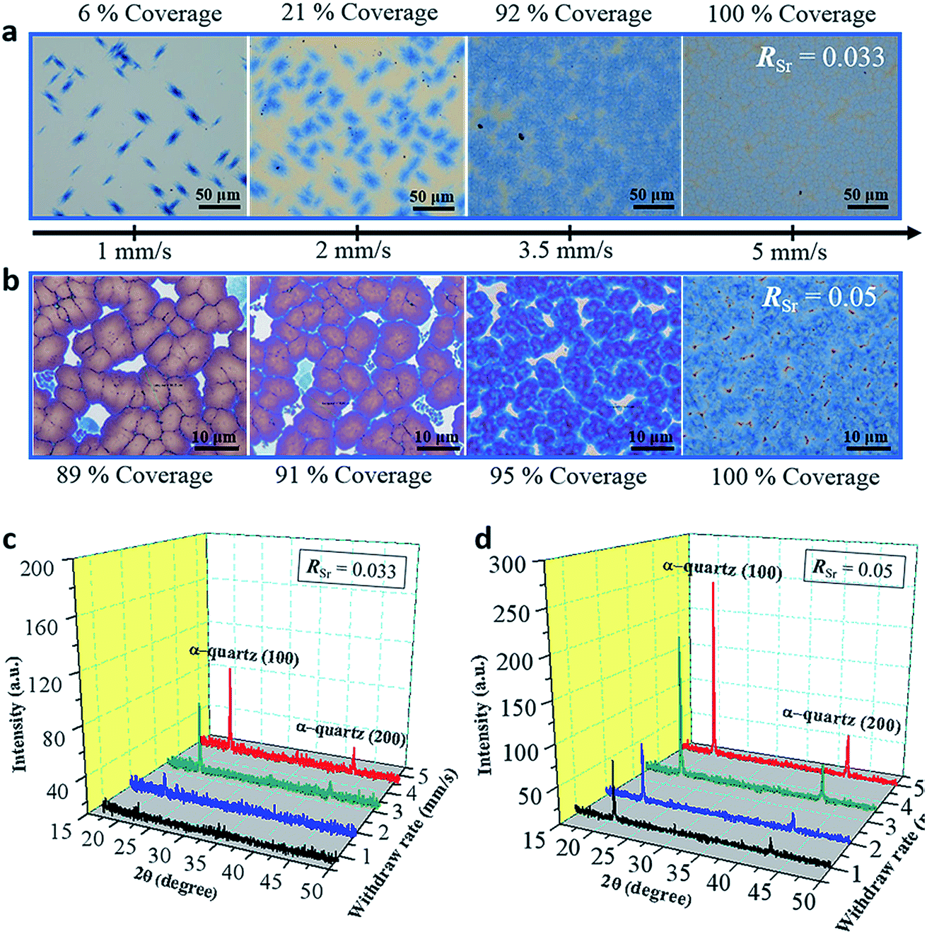 | ||
| Fig. 4 Thickness study for the as-prepared film: (a and b) optical images of films prepared with different withdrawal speeds (indicated in the axis below the images) for RSr = 0.033 (a) and RSr = 0.05 (b). The areal coverages of the porous α-quartz phase for (a) and that of dense α-quartz crystals for (b) are indicated next to the images respectively. The corresponding XRD θ–2θ measurements are shown in (c) and (d) for the RSr = 0.033 and RSr = 0.05 series, respectively. Those films were prepared in a relative humidity of 40% at 25 °C using Brij-58 as the surfactant. The annealing treatment was at 1000 °C for 300 minutes in an air atmosphere. | ||
In Fig. 4a the color contrast allows distinguishing the amorphous areas (with lighter tones) from areas covered by α-quartz (in blue tones). In Fig. 4b the films are fully crystallized and the color contrast allows determining the % coverage by dense α-quartz (zones with darker contrast). It can be observed that the crystallized areas increase with higher Uw for the RSr = 0.033 series. This trend is also reflected in the XRD patterns of the films which display higher intensities of the α-quartz (00L) reflections for increasing withdrawal speeds (Fig. 4c). In the case of the RSr = 0.05 series, XRD also shows an increasing intensity for higher Uw, but in this case this is due to the higher surface coverage by large α-quartz crystals with a lower mosaicity (see Fig. S12†). These results reflect the influence of the total amount of Sr in the films which, within a series of constant RSr, is proportional to the film thickness. In particular, for RSr = 0.033 we can conclude that fully crystallized films with a 100% surface coverage cannot be obtained for film thicknesses below 200 nm. Analogously, in the case of RSr = 0.05, 200 nm is the minimum thickness to achieve a high coverage (≥95%) of dense α-quartz. These results point to the existence of a threshold in the total amount of Sr that is necessary to obtain homogeneous microstructures of porous (RSr = 0.033) and dense (RSr = 0.05) α-quartz.
3.3 Multi-layer film synthesis
To exploit epitaxial α-quartz films in technological applications it is essential to increase the film thicknesses towards the micron range. To this aim we investigated the suitability of a multi-layer deposition approach: the sequential deposition and consolidation of several gel layers before a final annealing treatment to induce the epitaxial α-quartz growth. Fig. 5a presents a series of SEM images corresponding to the cross-sections of films consisting of 1 to 5 layers after the crystallization treatment. One cannot distinguish the interfaces between successive layers and the thickness of the films increases linearly with the number of layers, reaching about 800 nm for the sample consisting of 5 layers (see Fig. 5b). From the XRD measurements of Fig. 5c we can see that all the films present the usual α-quartz (100) out of plane texture and that the intensity of the reflections is proportional to the number of layers of the film. This indicates that the successive layers maintain the crystallinity and crystal orientation with an excellent homogeneity over areas of several cm2. Indeed, we have obtained XRD maps on a 5-layer film deposited on a 2-inch Si wafer, showing very slight variations of the α-quartz (100) reflection intensity and the FWHM of the rocking curve over a large area (see Fig. S13†). The intensity of rocking curves of the (100) reflection is also larger for the thicker films and the FWHM is close to 2° for all the films. This shows that the multi-layer approach is not detrimental to the growth of α-quartz films. Further confirmation of this is given by the pole figure of the 5-layer film presented in the inset of Fig. 5b which confirms that the multi-layer synthesis preserves the epitaxial growth of the first layer. It has been argued33 that in many inorganic films prepared by chemical solution deposition the maximum achievable thickness is imposed by the cracks due to the lateral tensile stresses which appear during the densification of the layers. With our multi-layer deposition approach we have circumvented this issue by performing a treatment to consolidate the gel layer (450 °C for 10 min in an air atmosphere) after each deposition (see the Experimental section for more details).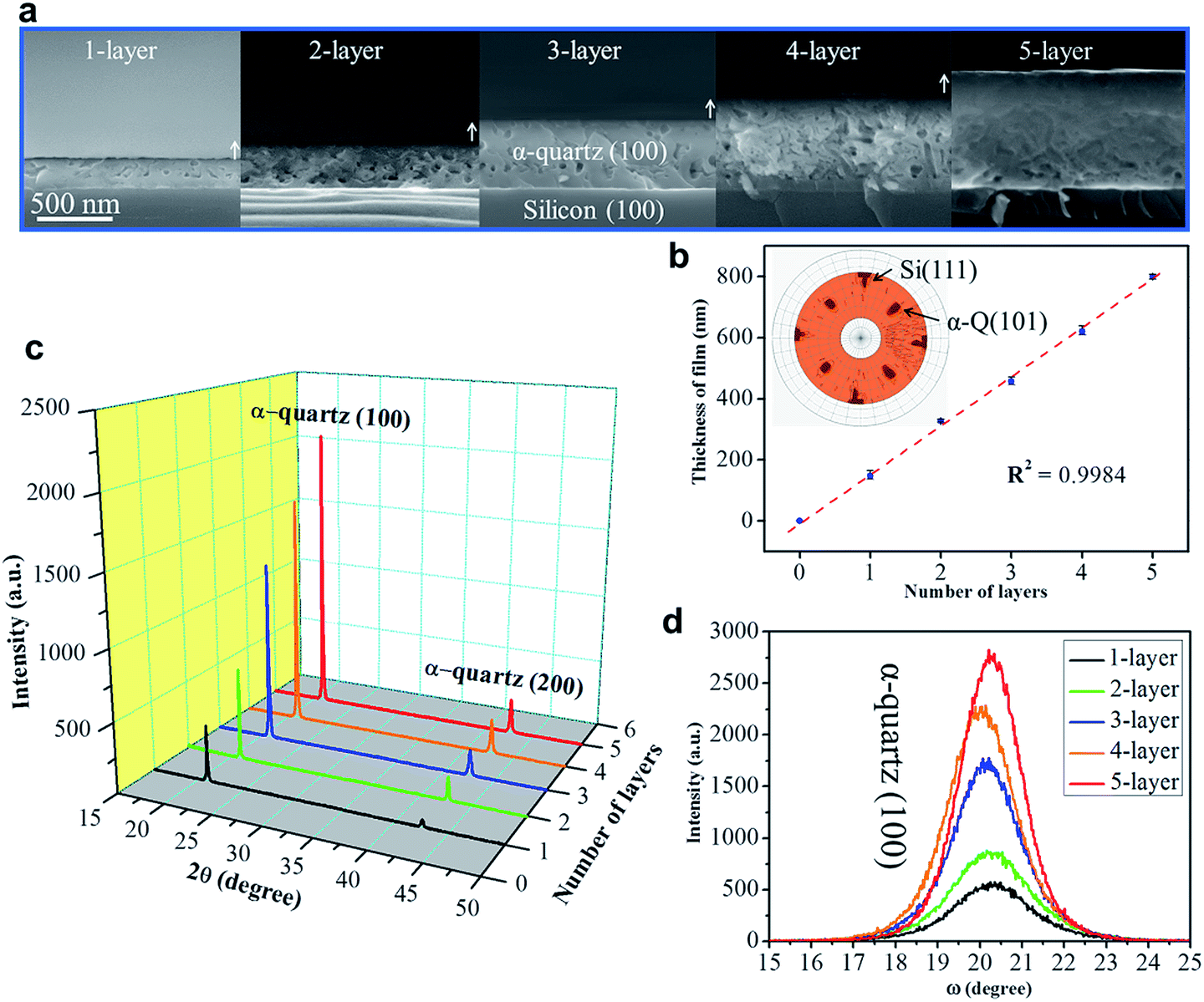 | ||
| Fig. 5 (a) SEM images of the cross-section of the films with different numbers of layers. (b) The linear increase of thickness with the addition of the number of layers; the inserted image is the pole figure for the 5-layer film to show that the epitaxial growth is maintained. (c) XRD θ–2θ scan showing the linear increase of α-quartz (100) reflections as the number of layers increases. (d) The rocking curves for different multi-layer samples. To prepare these films, all the gel layers were deposited in a relative humidity of 40% at 25 °C with RSr = 0.05 and using Brij-58 as the surfactant. The annealing treatment was at 1000 °C for 300 minutes in an air atmosphere. | ||
The availability of epitaxial quartz films with thicknesses approaching a micron made us attempt an unprecedented characterization of the piezoelectric properties by the direct piezoelectric effect. To this aim we employed a novel technique, direct piezoelectric force microscopy (DPFM). In DPFM a conductive AFM tip strains a piezoelectric while the charge that is built up by the mechanical stress induced to the material is being measured.20 In order to characterize the piezoelectric response of α-quartz films we performed a step-like force function applied to the material under tests, see Fig. 6a.
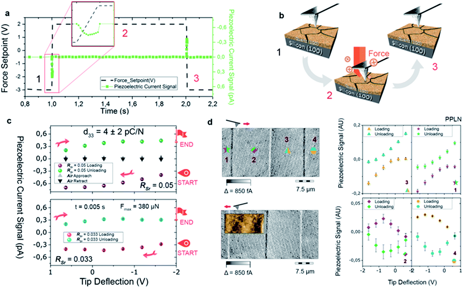 | ||
| Fig. 6 Force and piezoelectric current vs. time (s) for different applied forces for a quartz film with RSr = 0.05 (a). The current peaks are seen when DPFM-Si and DPFM-So of a Periodically Poled Lithium Niobate (PPLN) showing the ferroelectric domain configuration of the test sample that is used as a reference for calibration. Scheme of the spectroscopy experiments carried out in which the AFM tip applies a suitable force, within a given time, collecting the charges generated by the direct piezoelectric effect (b). Curves obtained for α-quartz films with RSr = 0.05 and RSr = 0.033 showing their piezoelectric response (c). The graphs were obtained by averaging 4 × 4 matrix volume spectroscopy experiments in an area of 10 microns, in order to depict the homogeneity of the sample. Results of the spectroscopy experiments obtained in four different locations on the PPLN test sample, indicated by the numbers 1 to 4 and the corresponding spots where the curves were recorded (d). Minutes in an air atmosphere. | ||
The force profile starts with a constant value, while at 1 s the force is increased to a value of 380 μN in a 5 ms time step. Following this step, a constant force is re-settled for an additional 1 s, while at 2 s, an unloading ramp is performed, reducing the applied force. While force is varied, the current channel is recorded simultaneously; current is depicted in green squares in Fig. 6a. Due to the piezoelectric effect, a constant force builds up a constant charge, and hence the recorded current remains zero. However, when the force is varied, through a loading or unloading event, there is an increase or decrease of the charge build up, whereas a constant current can be seen at a constant force rate applied, see Fig. 6b. The system current is calibrated using a known resistance, while the force applied is calibrated using standard procedures available for AFM. To increase homogeneity, the results of our experiments are depicted by averaging 10 curves obtained in 10 different randomized spots of the sample, see Fig. 6c. We were able to obtain the d33 value of the material by simply dividing the collected current, in pC s−1 units, by the force rate applied (0.078 N s−1), obtaining the piezoelectric constant in pC N−1. Independently of the RSr value, a similar piezoelectric response is measured. As a negative test, we repeated the movement of the Z-piezo of the AFM (see black-and-grey triangles of Fig. 6c), obtaining a zero-current response. We performed another test experiment in a ferroelectric Periodically Poled Lithium Niobate (PPLN) sample as a reference (see Fig. 6d). For obtaining the location of ferroelectric domains, DPFM-Si (Signal Input) and DPFM-So (Signal Output) scans are recorded, revealing the expected antiparallel domain configuration.20 A similar force ramp consisting of loading and unloading the sample surface with the AFM tip is repeated in each of the domain positions (see Fig. 6d in which the numbers are correlated with right panel graphs). It is seen that the current reverses depending on which domain polarization direction is mechanically stressed. Such behavior is expected for a ferroelectric known sample, leading us to conclude that the recorded current signal arises from the piezoelectric properties inherent to our films. From these measurements we obtained a d33 of 4 ± 2 pC N−1. The reference piezoelectric constants of bulk quartz are d11 = 2.3 pC N−1 and d14 = −0.7 pC N−1.34 Since the out of plane orientation of our films is [210] (i.e. at 30° with respect to [100]) the obtained piezoelectric constant is in reasonably good agreement with d11 of bulk quartz (i.e. measured along [100]).
3.4 Nanostructuring epitaxial quartz films
The enhanced control over the crystallization of epitaxial quartz and the multi-layer deposition approach has enabled us to achieve integrated epitaxial quartz structures on silicon. We demonstrate the feasibility of this integration by combining the dip-coating process to synthesize multi-layers of silica xerogels on silicon (100) substrates, with two complementary patterning techniques. By Laser Interference Lithography we generated silicon masters of highly controlled size, height and pitch of vertical pillars, from which we produced PDMS molds. The molds were used to pattern amorphous silica multi-layers by soft imprint lithography in a fast process which does not require lithographic masks and allows obtaining a precise control of the dimensions over large surfaces (see Fig. S14†).To illustrate the possibilities of this approach we prepared cm-scale areas of epitaxial quartz patterned with pillars on a multi-deposition silica film with four layers. Fig. 7a and b show different magnification SEM-FEG images of a patterned quartz film displaying pillars of 1 μm diameter and 2 μm in height. The optical image of the whole patterned film presented in the lower-right inset of Fig. 7a displays the characteristic wavelength-selective reflectance of 2D-photonic crystals, indicating the good quality of the patterning over an area of several square centimeters. The electron diffraction of a single column (Fig. 7c) and X-ray diffraction θ–2θ and ω scans of the film (Fig. 7d) show that, as in non-patterned films, it consists of epitaxial quartz with Si (100)//α-quartz (100) and Si (010)//α-quartz (010). It is noteworthy that the epitaxial growth has been transferred to the pillars. With regard to these, the multi-layer deposition approach is highly relevant because the first three silica layers act as crystallization seeds and facilitate the adhesion of the fourth layer to faultlessly replicate the columnar shapes when it is imprinted by the PDMS mold. The process to prepare patterned epitaxial quartz (Fig. 7e) involves a first step of imprinting a Sr-doped amorphous SiO2 gel followed by a crystallization treatment at high temperature. Comparing the patterned films before (Fig. S13b and c†) and after (Fig. 7b) crystallization one can see that the shape of the patterned structures is highly preserved during the whole process. Indeed, no cracks or other defects are generated upon crystallization, in spite of the substantial thermal stresses that can be developed for pillar dimensions exceeding 1 μm and temperature differences in the order of 1000 °C. If the multi-layer deposition approach allows preparing thicker epitaxial films above 500 nm (see Section 3.3), we have shown that in combination with soft imprint lithography it is possible to obtain features with vertical dimensions in the micron range.
 | ||
| Fig. 7 Patterning and crystallization of Sr-doped silica multilayers by soft imprint lithography. (a) FEG-SEM image of the epitaxial quartz columnar pattern. The inset figures show higher magnification FEG-SEM images illustrating the morphology of the quartz columns. The right-down inset corresponds to an optical image of the film which displays the characteristic wavelength reflectance selectivity of a 2-D photonic crystal. (b) Cross-sectional SEM image of a quartz column grown on the Si substrate assisted by the Sr2+ catalyst at 1000 °C, 5 hours. (c) Transmission Electron Microscopy image and electron diffraction measurement (inset image) of the α-quartz/Si interface of a single column. (d) θ–2θ XRD pattern displaying the out of plane texture of the (100) α-quartz crystallographic phase in the patterned film. The inset shows a rocking curve indicating that the mosaicity value of quartz is not affected by the lithography process. (e) Schematics summarizing the key steps that were applied to produce patterned epitaxial quartz films by soft imprint lithography. | ||
4. Conclusions
We have shown that the total amount of devitrifying agent in mesoporous silica films prepared by dip-coating determines the microstructure of epitaxial α-quartz after thermal devitrification. In our study the quantity of Sr2+ was controlled by both the ratio of Sr2+ to SiO2 (RSr) and the withdrawal speed (Uw) during dip-coating. In particular, with Uw = 5 mm s−1, for RSr = 0.033 one obtains porous α-quartz films with randomly distributed macropores of sizes below 300 nm. In contrast for RSr ≥ 0.05 the microstructure is dominated by dense α-quartz crystals of several microns in size. Our study has also established the importance of controlling the relative humidity and the nature of the surfactant. We achieved the targeted microstructures (porous or dense α-quartz epitaxial films) with a relative humidity of 40% and using the non-ionic surfactant Brij-58. The possibility of controlling these contrasting microstructures by simply adjusting the content of devitrifying agent paves the way for further developments exploiting the potentialities of α-quartz films on Si (100) for specific applications. Namely, the films displaying larger dense α-quartz structures are best placed for the development of optical devices as the size of the crystals is sufficiently large to enable the fabrication of photonic structures by lithographic techniques. In contrast, the porous films are well-suited for microgravimetric sensing applications as the pores can be further functionalized to provide an enhanced selectivity towards analytes and increase the selectivity and detection limits. An additional step forward towards these sensing applications is the suitability of the multi-layer synthesis to extend the thickness of the α-quartz films prepared by dip-coating. By combining this method with soft imprint lithography, we have demonstrated that one can obtain patterned epitaxial quartz films. These findings open up new horizons for integration of quartz-based nanostructures on silicon from which many applications relying on electromechanics, optics and optomechanics would benefit.Conflicts of interest
There are no conflicts to declare.Acknowledgements
This project has received funding from the European Research Council (ERC) under the European Union's Horizon 2020 research and innovation programme (No. 803004); the French Agence Nationale de la Recherche (ANR), project Q-NOSS ANR ANR-16-CE09-0006-01; the Spanish Ministry of Science Innovation and Universities in co-funding with European Social funds through the Severo Ochoa Program for Centers of Excellence in R&D (SEV-2015-0496) and the Ramón y Cajal program (J. G., RyC-2012-11709); the Generalitat de Catalunya (2017SGR00765). Q. Z. was financially supported by the China Scholarship Council (CSC) with No. 201506060170. Q. Z.'s work was done as a part of the Ph.D program in Materials Science at Universitat Autònoma de Barcelona. The authors thank the “Laboratorio de Microscopías Avanzadas-Instituto de Nanociencia de Aragón” for offering their expertise in the preparation of TEM cross-sections. A. Crespi from ICMAB XRD diffraction service is acknowledged for pole figure measurements. The authors also thank Judith Oró from the ICMAB microscopy service. The FEGSEM instrumentation was facilitated by the Institut des Matériaux de Paris Centre (IMPC FR2482) and was funded by Sorbonne Université, CNRS and by the C'Nano projects of the Région Ile-de-France. We thank David Montero for performing the FEGSEM images. Microscopy work was conducted at the Center for Nanophase Materials Sciences, which is a DOE Office of Science User Facility.References
- C. L. Melcher and J. S. Schweitzer, Cerium-Doped Lutetium Oxyorthosilicate – A Fast, Efficient New Scintillator, IEEE Trans. Nucl. Sci., 1992, 39(4), 502–505 CrossRef CAS.
- G. Sauerbrey, Verwendung Von Schwingquarzen Zur Wagung Dunner Schichten Und Zur Mikrowagung, Z. Phys., 1959, 155(2), 206–222 CrossRef CAS.
- E. Benes, M. Groschl, W. Burger and M. Schmid, Sensors based on piezoelectric resonators, Sens. Actuators, A, 1995, 48(1), 1–21 CrossRef CAS.
- R. E. Newnham, Properties of Materials: Anisotropy, Symmetry, Structure, Oxford U. Press, New York, 2005 Search PubMed.
- P. Richet, Y. Bottinga, L. Denielou, J. P. Petitet and C. Tequi, Thermodynamic Properties of Quartz, Cristobalite and Amorphous SiO2 – Drop Calorimetry Measurements Between 1000 K and 1800 K and a Review from 0 K to 2000 K, Geochim. Cosmochim. Acta, 1982, 46(12), 2639–2658 CrossRef CAS.
- H. J. Freund, Controlling Silica in Its Crystalline and Amorphous States: A Problem in Surface Science, Acc. Chem. Res., 2017, 50(3), 446–449 CrossRef CAS PubMed.
- C. Buchner, L. Lichtenstein, X. Yu, J. A. Boscoboinik, B. Yang and W. E. Kaden, et al., Ultrathin silica films: the atomic structure of two-dimensional crystals and glasses, Chemistry, 2014, 20(30), 9176–9183 CrossRef PubMed.
- A. Carretero-Genevrier, M. Gich, L. Picas, J. Gazquez, G. L. Drisko and C. Boissiere, et al., Soft-chemistry-based routes to epitaxial alpha-quartz thin films with tunable textures, Science, 2013, 340(6134), 827–831 CrossRef CAS PubMed.
- G. L. Drisko, A. Carretero-Genevrier, M. Gich, J. Gàzquez, D. Ferrah and D. Grosso, et al., Water-Induced Phase Separation Forming Macrostructured Epitaxial Quartz Films on Silicon, Adv. Funct. Mater., 2014, 24(35), 5494–5502 CrossRef CAS.
- G. L. Drisko, A. Carretero-Genevrier, A. Perrot, M. Gich, J. Gazquez and J. Rodriguez-Carvajal, et al., Crystallization of hollow mesoporous silica nanoparticles, Chem. Commun., 2015, 51(20), 4164–4167 RSC.
- T. Matsuno, Y. Kuroda, M. Kitahara, A. Shimojima, H. Wada and K. Kuroda, A Single-Crystalline Mesoporous Quartz Superlattice, Angew. Chem., Int. Ed., 2016, 55(20), 6008–6012 CrossRef CAS PubMed.
- A. Ndayishimiye, A. Largeteau, M. Prakasam, S. Pechev, M.-A. Dourges and G. Goglio, Low temperature hydrothermal sintering process for the quasi-complete densification of nanometric α-quartz, Scr. Mater., 2018, 145, 118–121 CrossRef CAS.
- L. Li, H. Tissot, S. Shaikhutdinov and H.-J. Freund, Transition Metal Induced Crystallization of Ultrathin Silica Films, Chem. Mater., 2017, 29(3), 931–934 CrossRef CAS.
- M. Mandal, V. Stagno, Y. Fei and K. Landskron, Investigation of High-Pressure and Temperature Behavior of Surfactant-Containing Periodic Mesostructured Silicas, Cryst. Growth Des., 2012, 13(1), 15–18 CrossRef.
- F. Putz, S. Scherer, M. Ober, R. Morak, O. Paris and N. Hüsing, 3D Printing of Hierarchical Porous Silica and α-Quartz, Adv. Mater. Technol., 2018, 3, 180060 Search PubMed.
- Y.-I. Sohn, R. Miller, V. Venkataraman and M. Lončar, Mechanical and optical nanodevices in single-crystal quartz, Appl. Phys. Lett., 2017, 111(26), 263103 CrossRef.
- A. Carretero-Genevrier and M. Gich, Preparation of Macroporous Epitaxial Quartz Films on Silicon by Chemical Solution Deposition, JoVE, 2015, 106, e53543 Search PubMed.
- Z. Santybayeva, A. Meghit, R. Desgarceaux, R. Teissier, F. Pichot and C. de Marin, et al., Fabrication of quartz microcylinders by laser interference lithography for angular optical tweezers, J. Micro/Nanolithogr., MEMS, MOEMS, 2016, 15(3), 034507 CrossRef.
- J. Schindelin, I. Arganda-Carreras, E. Frise, V. Kaynig, M. Longair and T. Pietzsch, et al., Fiji: an open-source platform for biological-image analysis, Nat. Methods, 2012, 9, 676 CrossRef CAS PubMed.
- A. Gomez, M. Gich, A. Carretero-Genevrier, T. Puig and X. Obradors, Piezo-generated charge mapping revealed through direct piezoelectric force microscopy, Nat. Commun., 2017, 8(1), 1113 CrossRef CAS PubMed.
- D. Necas and P. Klapetek, Gwyddion: an open-source software for SPM data analysis, Cent. Eur. J. Phys., 2012, 10(1), 181–188 Search PubMed.
- The Merck Index, ed. S. Budavari, Merck Research Laboratories, Whitehouse Station, 12th edn, 1996 Search PubMed.
- M. Gustafsson, F. Roccaforte, J. Keinonen, W. Bolse, L. Ziegeler and K. P. Lieb, Oxygen-activated epitaxial recrystallization of Li-implanted alpha-SiO2, Phys. Rev. B: Condens. Matter Mater. Phys., 2000, 61(5), 3327–3332 CrossRef CAS.
- S. Gąsiorek, S. Dhar, K. P. Lieb and P. Schaaf, Laser-induced epitaxial recrystallization after alkali-ion implantion into α-quartz, Appl. Surf. Sci., 2005, 247(1–4), 396–400 CrossRef.
- S. Dhar, P. K. Sahoo, S. Gąsiorek, U. Vetter, V. N. Kulkarni and K. P. Lieb, Cathodoluminescence and solid phase epitaxy in Ba-irradiated α-quartz, J. Appl. Phys., 2005, 97(1) CrossRef.
- J. Keinonen, S. Gąsiorek, P. K. Sahoo, S. Dhar and K. P. Lieb, Light-emitting defects and epitaxy in alkali-ion-implanted α quartz, Appl. Phys. Lett., 2006, 88(26), 261102 CrossRef.
- S. Hayashi, M. Sugai, Z. Nakagawa, T. Takei, K. Kawasaki and T. Katsuyama, et al., Preparation of CaSiO3 whiskers from alkali halide fluxes, J. Eur. Ceram. Soc., 2000, 20(8), 1099–1103 CrossRef CAS.
- A. C. Tas, Molten salt synthesis of calcium hydroxyapatite whiskers, J. Am. Ceram. Soc., 2001, 84(2), 295–300 CrossRef CAS.
- W. Wang, C. Xu, X. Wang, Y. Liu, Y. Zhan and C. Zheng, et al., Preparation of SnO2 nanorods by annealing SnO2 powder in NaCl flux, J. Mater. Chem., 2002, 12(6), 1922–1925 RSC.
- W. Z. Wang, L. J. Wang, L. Liu, C. He, J. Tan and Y. J. Liang, Morphology-controlled synthesis and growth mechanism of ZnO nanostructures via the NaCl nonaqueous ionic liquid route, CrystEngComm, 2012, 14(15), 4997–5004 RSC.
- L. Landau and B. Levich, Dragging of a liquid by a moving plate, Acta Physicochim. URSS, 1942, 17, 42–54 Search PubMed.
- M. Faustini, B. Louis, P. A. Albouy, M. Kuemmel and D. Grosso, Preparation of Sol–Gel Films by Dip-Coating in Extreme Conditions, J. Phys. Chem. C, 2010, 114(17), 7637–7645 CrossRef CAS.
- D. Grosso, How to exploit the full potential of the dip-coating process to better control film formation, J. Mater. Chem., 2011, 21(43), 17033–17038 RSC.
- R. Bechmann, Elastic and Piezoelectric Constants of Alpha-Quartz, Phys. Rev., 1958, 110(5), 1060–1061 CrossRef.
Footnote |
| † Electronic supplementary information (ESI) available. See DOI: 10.1039/c9na00388f |
| This journal is © The Royal Society of Chemistry 2019 |