
 Open Access Article
 This Open Access Article is licensed under a Creative Commons Attribution-Non Commercial 3.0 Unported Licence
Transformation of threshold volatile switching to quantum point contact originated nonvolatile switching in graphene interface controlled memory devices†
Zuheng
Wu
abc,
Xiaolong
Zhao
a,
Yang
Yang
ab,
Wei
Wang
a,
Xumeng
Zhang
abc,
Rui
Wang
abc,
Rongrong
Cao
abc,
Qi
Liu
ac and
Writam
Banerjee
 *acd
*acd
aKey Laboratory of Microelectronics Devices & Integrated Technology, Institute of Microelectronics, Chinese Academy of Sciences, No. 3, BeiTuCheng West Road, ChaoYang District, Beijing 100029, P. R. China
bUniversity of Chinese Academy of Sciences, No. 19(A) Yuquan Road, Shijingshan District, Beijing, P.R.China 100049
cJiangsu National Synergetic Innovation Center for Advanced Materials (SICAM), Nanjing 210009, P. R. China
dDepartment of Material Science and Engineering, Pohang University of Science and Technology (POSTECH), Pohang 790-784, Republic of Korea. E-mail: writam@postech.ac.kr
First published on 6th August 2019
Abstract
Resistive switching devices based on binary transition metal oxides have been widely investigated. However, these devices invariably manifest threshold switching characteristics when the active metal electrode is silver, the dielectric layer is hafnium oxide and platinum is used as the bottom electrode, and have a relatively low compliance current (<100 μA). Here we developed a way to transform an Ag-based hafnium oxide selector into quantum-contact originated memory with a low compliance current, in which a graphene interface barrier layer is inserted between the silver electrode and hafnium oxide layer. Devices with structure Ag/HfOx/Pt acts as a bipolar selector with a high selectivity of >108 and sub-threshold swing of ∼1 mV dec−1. After introducing a graphene interface barrier, high stress dependent (forming at +3 V) formation of localized conducting filaments embodies stable nonvolatile memory characteristics with low set/reset voltages (<±1.0 V), low reset power (6 μW) and multi-level potential. Grain boundaries of the graphene interface control the type of switching in the devices. A good barrier can switch the Ag-based volatile selector into Ag-based nonvolatile memory.
Introduction
Resistive random access memory (RRAM) devices are widely considered for ultra-high density nonvolatile memory application due to plenty of advantages (e.g., high speed, low power consumption, potential for high density integration etc.).1–3 Both anionic and cationic motion based RRAM devices have their own merits of applicability. Cation-based resistive switching (RS) devices transform between a high resistance state (HRS) and a low resistance state (LRS) typically with the structure of active top electrode (TE)/RS dielectric layer/inert bottom electrode (BE). The switching mechanism of these devices is dominated by conductive filament (CF) formation/dissolution, namely electrochemical metallization (ECM).4,5 The physical switching mechanism for the formation/dissolution of these CFs is due to effect of electric field and Joule heating processes.In ECM, silver is an established active electrode or dopant material, and invariably exerts threshold switching (TS) characteristics at a low compliance current, as has been reported by several groups.6,7 Due to the thermal diffusion of the active ions under conditions of an imposed electric field, the temporal and special evolution of the metallic bridge conducted the conductance evolution process in such devices.8,9 Applying a voltage to set the device, the device converts from a HRS into a LRS when reaching to a certain voltage namely the threshold voltage (Vth). Whereas retracing the voltage sweep, the device returns to a HRS at a certain voltage namely the hold voltage (Vh). Below a certain critical voltage the device is incapable of maintaining a LRS after revoking the external stimuli. However, instead of showing a volatile TS nature, the ECM devices can also manifest a nonvolatile memory switch (MS) depending on the stability and retention capability of the CF.10–12 Although both the switches are dominated by the formation/dissolution of the CF, for a practical application the requirements for the MS and TS are poles apart. It’s a twist of fate that a MS must be a low power nonvolatile device with higher stability of the CF, whereas a TS must be a highly nonlinear volatile device with poor stability of the CF. Previously, Ag-based ECM devices with either MS type or TS type switching have been reported using several inorganic dielectrics.13–15 Depending on the different diffusion barriers of different dielectrics and dielectric based variable diffusion coefficient of cations, the anatomy of the CF can be changed. In general, the Ag/HfOx/Pt based structure is used to design TS type devices.16–19 However, it is also possible to obtain the MS behavior in the same structure by modulating the morphology of the CF using an ultra-thin graphene barrier layer. In our previous report, we have demonstrated Ag-based nonvolatile switching by creating nano-holes in a graphene barrier layer using expensive modern photolithographic technique. However, in this work the graphene barrier layers can effectively switch the volatile selector into nonvolatile memory using a simple cost effective approach.
In this work, we investigated graphene as an interface barrier layer to modify the performances of Ag-based RRAM devices with low compliance current. Graphene is a very stable, semitransparent, very thin sheet with periodically tightly packed carbon atoms with sp2 hybridization. Structurally, a graphene sheet has a two-dimensional hexagonal grid structure with 65 pm diameter of cavity.20–22 Because of the smaller cavity size as compared to any other atoms or ions, graphene has proved to be a very effective and thermally stable to ∼750 °C atomic diffusion barrier material.23 Previously, graphene as a barrier layer has been successfully used to reduce the power for anionic CF based devices.24,25 But it is more challenging to change the entire switching nature from a highly nonlinear volatile TS to a low power operated nonvolatile MS, in the same HfOx based RRAM structure. Here, Ag/HfOx/Pt based standard devices have been used to achieve a lower operating voltage controlled (±0.3 V) volatile TS with a highly stable nonlinearity of >108. The TS nature of the same device changes to MS when a graphene layer is introduced as a barrier at the Ag/HfOx interface. A high initial stress dependent forming process (+3 V @ 100 μA) can create a localized hole in the graphene layer which can actively control the diffusion process of the Ag cations into the HfOx matrix, hence the anatomy of the CF can be controlled. A highly stable low voltage (<±1.0 V) operated nonvolatile MS performance of the graphene-based Ag/HfOx devices is achieved with a large resistance ratio (∼102), multi-level storage capacity with a lower operating power to a few μW. Moreover, the authenticity of the claimed performances was verified by re-fabricating the complete stack of the graphene-based devices. Precaution must be taken during the graphene film transfer process, as it can introduce different sizes of grains which can originate either the MS or the TS nature in device-to-device variation. In this paper, the detailed physical analysis for all possible contingencies are examined and discussed, which can definitely provide guidance for future development.
Experimental
The Pt/Ag/HfOx/Pt/Ti (D1) devices were fabricated with crossbar structures. First, after the first ultraviolet lithography process, a Pt/Ti (40/5 nm) BE was successively deposited by e-beam evaporation onto the SiO2/Si wafer followed by a lift-off process. Then, a 5 nm HfOx film was deposited by the magnetron sputtering method. Finally, after the second ultraviolet lithography process, 40 nm Ag TE was deposited with a 10 nm Pt capping layer by the magnetron sputtering method, and followed by a lift-off process. To fabricate the graphene-based Pt/Ag/graphene/HfOx/Pt/Ti (D2) devices, the graphene was transferred before TE deposition. Graphene sheet was purchased from Hefei Vigon Material Technology Co., Ltd. The graphene was deposited on two sides of a Cu film. At first, to protect the graphene, one side was coated by rotation (4000 rpm, 60 s) with a layer of PMMA. Next, oxygen plasma (1 Pa, O2 80 sccm, 100 W and 15 min) was used to etch the graphene which was not protected by PMMA. After the etching of graphene, FeCl3 was used for 6 hours to etch the Cu film. After that, hydrogen chloride solution was used to clean away FeCl3 (15 min, 3 times). Then, deionized water was used to clean away the hydrogen chloride (10 min, 3 times), and the cleaned graphene film was transferred onto HfOx film. Finally, an ultraviolet lithography process, followed by oxygen plasma etching process (0.8 Pa, O2 40 sccm, 50 W and 1 min), was used to pattern the graphene film. The fabrication process of the TiN/HfOx/Pt (D3) devices is reported somewhere else.24 In that case, a thin interfacial layer i.e. TiOx or TiON can be formed which can be influential for the switching process.26–29 However, in this work we are just focusing on the Ag-based devices i.e. D1 and D2.The DC mode and pulse mode I–V characteristics of all devices were implemented in the atmosphere using a semiconductor characterization system (Agilent B1500A Semiconductor Device Analyzer). The SEM images of the morphology of the corresponding devices were obtained using a field-emission scanning electron microscope (ZEISS SUPRA 55 SAPPHIRE). The HRTEM images and EDS line scan composition analysis was accomplished with a JEOL ARM 200F cold field emission gun TEM/STEM with cs-corrector under 200 kV voltage.
Results and discussion
To illustrate the proposed idea, we have designed both ECM and VCM (valence change mechanism) type RRAM devices maintaining the same 5 nm thick HfOx film as the RS dielectric layer and Pt as the inert electrode material. The only differences among the different structures are in the TE layer and the graphene layer, which clearly demonstrate that the graphene barrier could induce selector to transform into memory. Three types of structures are identified as D1, D2, and D3 for Ag/HfOx/Pt, Ag/graphene/HfOx/Pt, and TiN/HfOx/Pt, respectively. Fig. 1a shows a schematic view of Ag-based standard selector devices (D1), which can perform a TS from low (Fig. 1b) to high (Fig. 1c) current compliances, induced by silver diffusion and drift motion. Previously similar TS behavior has been reported not only for Ag/HfOx based devices30 but also for flexible solution-processed devices.31 Selector can turn into memory when a graphene barrier layer is inserted between the HfOx layer and Ag-electrode (D2), as shown schematically in Fig. 1d. Diffusion of Ag into the HfOx layer can be controlled by the graphene barrier layer, which leads to transformation of TS behavior into resistive MS behavior. Fig. 1e and f show the I–V curves of D2 with 30 μA and 75 μA, respectively. A positive voltage was applied to the top Ag-electrode to switch the device from HRS to LRS. On the contrary, a negative voltage was used to reset the device. It is notable that the reset current in the D2 devices is scaling down with the decreasing compliance current (ICC). To confirm the similarity of MS in the D2 devices with the standard MS RRAM, we fabricated TiN/HfOx/Pt based VCM type D3 devices as shown in the schematic of Fig. 1g. The representative I–V characteristics at 30 μA (Fig. 1h) and 75 μA (Fig. 1i) show similar ICC dependent evolution of filament, which is discussed in our previous work.24 However, due to the involvement of oxygen vacancies, the more gradual reset nature of the D3 devices differs from the ionic-motion involved switching in D2 devices. Hence, in short the complete study is going to reveal the effect of graphene to transform a strictly volatile Ag-based switching into a nonvolatile one. To elucidate the proposal, the following discussion is going to be concentrated mostly on the Ag-based devices.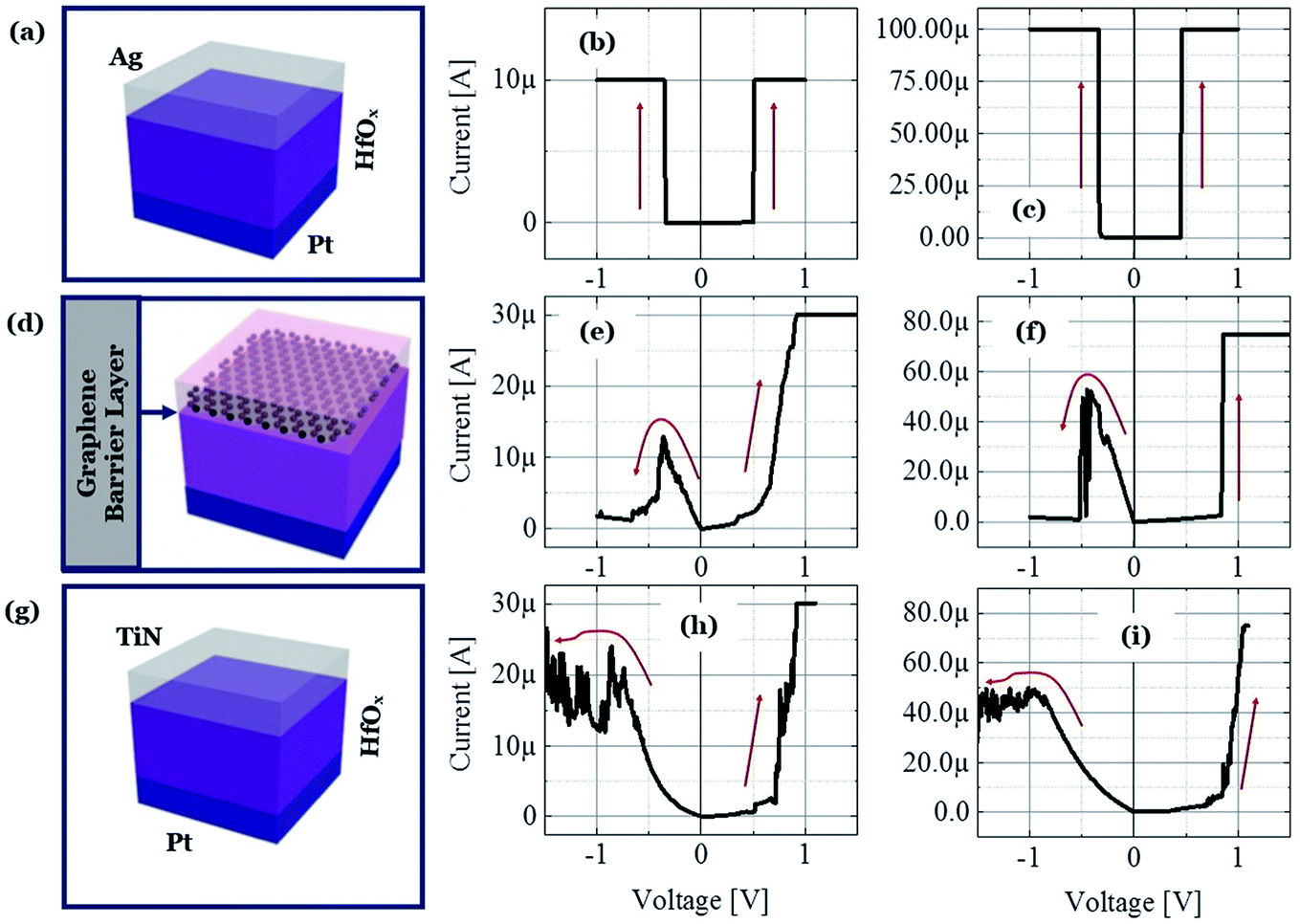 | ||
| Fig. 1 Comparison of resistive switching processes. (a) Schematic of D1 devices which can perform like a selector at (b) 10 μA and (c) 100 μA. (d) Illustration of the graphene barrier layer device D2 with memory behavior at (e) 30 μA and (f) 75 μA. (g) Illustration of D3 VCM devices, which can perform memory switching at (h) 30 μA and (i) 75 μA. However, because of a different switching mechanism, the set and reset processes of the D3 devices are different from D2 devices. | ||
To understand the graphene induced transformation from TS to MS, it is important to analyse the behavior of Ag-based non-graphene devices. The D1 device without a graphene barrier layer embodies perfect selector performance. Fig. 2a reflects the cycle-to-cycle I–V curve of an Ag-based selector with ICC of 10 nA (black), 50 μA (red), and 200 μA (blue) respectively, which shows very highly uniform selectivity/nonlinearity η of ION/IOFF ∼108. The bias polarity independent abrupt transition from the OFF to ON state is indicating the volatile nature of the performance. Fig. 2b plots the average selectivity of this selector with ICC from 50 pA to 300 μA in a log–log coordinate. What is worthy to note is that the η of the selector changes linearly with the ICC and there is no abrupt fluctuation indicating that the device is equipped with excellent selectivity of >108. Sub-threshold swing is another major criterion that defines how quickly a selector device can switch from the low current OFF to high current ON state. As shown in Fig. 2c, the ICC independent sharp sub-threshold swing of ∼1 mV dec−1 is indicating the excellent electrical performance of the D1 devices. To verify the uniformity of devices, we have examined the device-to-device variation of the threshold voltage (Vth) of the Ag-selectors. Fig. 2d shows the cumulative distribution of threshold voltage of 15 devices at ICC of 100 μA. Remarkably, an average threshold switching voltage is about +0.34 V and −0.28 V with standard deviation of 0.021 and 0.016 for positive threshold switching voltage (Vth+) and negative threshold switching voltage (Vth−), respectively. Relatively small Vth with ultra-low power consumption is preferable to suppress the sneak pass current problem. To identify the high performance operation, the Ag-selector device went through continuous switching cycles. Fig. 2e shows the DC endurance of D1 devices with >1.5 × 10³ cycles. Hence, it is confirmed that the fabricated Ag/HfOx/Pt devices are well suitable for the bi-directional TS application.
 | ||
| Fig. 2 Selector performance analysis of D1 devices. (a) The cycle-to-cycle I–V characteristics with different ICC values of 10 nA (black), 50 μA (red) and 200 μA (blue). (b) The change of selectivity as a function of ICC. A large selectivity of 108 is achieved by the D1 devices. (c) Sub-threshold swing is very low ∼1 mV dec−1 and independent of ICC values. (d) Statistical distribution showing that on average, D1 devices can switch at a positive Vth+ of +0.34 ± 0.021 V and at a negative Vth− of −0.28 ± 0.016 V. (e) The selector performance is very stable even after the rigorous 1.5 × 10³ dc switching endurance. | ||
In this section we describe the characteristics of devices with a structure of Ag/graphene/HfOx/Pt. Previously graphene as interfacial layer was used to reduce the power of the RRAM cell and transform the switching mode from VCM to ECM type.32 Nevertheless, here, graphene at the Ag/HfOx interface can transform the entire switching mechanism from TS to MS mode in ECM devices. During the electrical measurements, stimuli was applied to the Ag-TE, and Pt-BE was grounded. Unlike, Ag-based D1 devices, the graphene-based D2 devices needed a forming process. Although, device-to-device forming voltage variation can be observed, on average +3.2 ± 0.52 V is needed to initially activate the D2 devices, as shown is Fig. 3a. The forming voltage of the D2 devices is very significant in identifying the switching mode in the D2 RRAM, which will be discussed later. A glimpse of the graphene barrier induced MS in D2 devices is shown with continuous switching cycles in Fig. 3b. The device shows typically bipolar MS behavior. When the DC voltage is swept from 0 to +1 V with a current of 100 μA, the resistance of the device abruptly switched from HRS to LRS due to the formation of a CF and maintained LRS when the voltage is swept back from 1 to 0 V with the introduction of a large resistance ratio of >102. With the negative voltage sweep, the resistance of the device maintained LRS at the beginning and then suddenly switched from LRS to HRS because of the dissolution of the CF. The memory performance of the D2 devices is tunable with the ICC. Different levels of storage are identified in Fig. 3c. Due to the evolution of stronger CF formation, a sufficiently low LRS is achieved at 100 μA, which changes towards the higher resistance side with decreasing ICC up to several tens of μA. The LRS of the switched devices indicates the formation of an atomically connected CF. A minimum of half-integer quantized conductance transitions  for n = 1, 2, 3, etc., is observed in the Ag/graphene/HfOx/Pt based devices (Fig. 3d). Most importantly, in spite of the set ICC value, the nature of the LRS in D2 devices is linear (with nonlinearity of <2) with Ohmic type conduction behavior, as shown in Fig. 3e. In contrast, the D3 devices were nonlinear type, due to the oxygen-vacancy based CF formation, as discussed in an earlier study.24 To study the reset properties of the D2 devices, we plotted the reset voltage and reset current in Fig. 3f. For any compliance, reset voltage and reset current are randomly distributed with device-to-device. However, the probability of changing the reset voltage and reset current towards the lower side decreases with the scaling of ICC. In this specific case, for a ICC of 30 μA, considering an average reset voltage of 0.4 V, a minimum achievable reset power
  of 6 μW is needed to shut-down a single point contact. As aforementioned in the set process, a higher compliance current leads to stronger and more stable CF, hence, a stronger electric field and higher Joule heating is needed to dissolve the CF at a higher ICC.
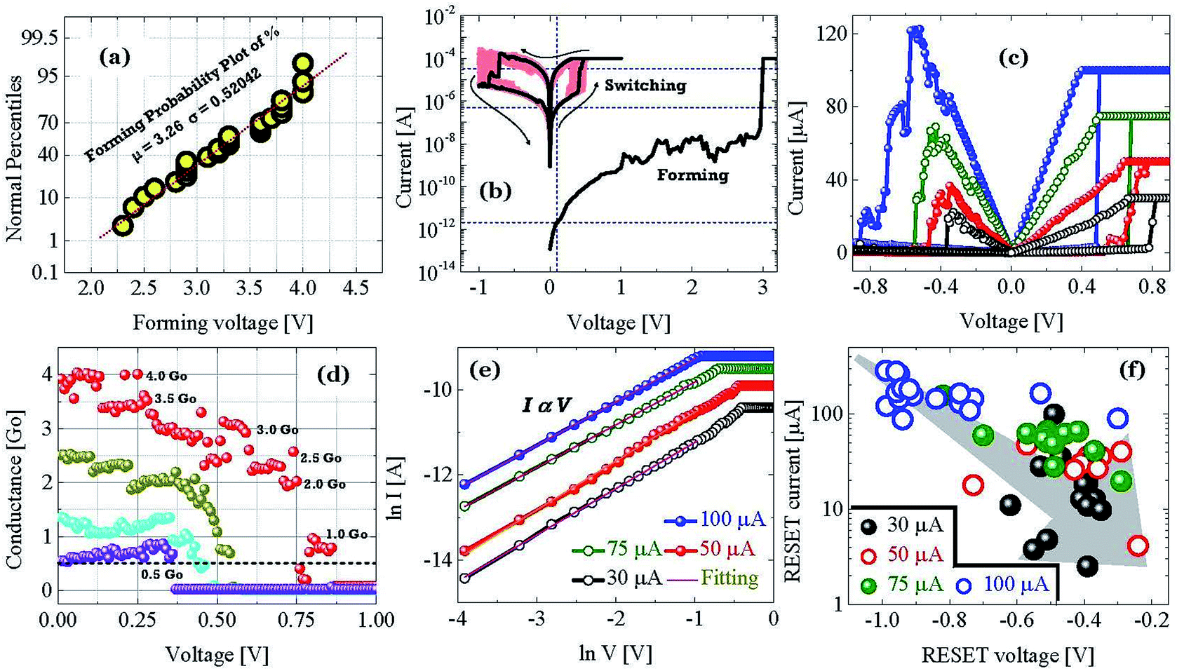 | ||
| Fig. 3 Performance analysis of Ag/graphene/HfOx/Pt devices and the origin of MS. (a) The device-to-device forming voltage distribution. (b) The continuous I–V characteristics at 100 μA. The black line shows a typical cycle. (c) The effect of ICC to define different levels of the devices. (d) A half integer quantum conductance change is identified. (e) Ohmic conduction is dominant in the LRS. (e) The variation of the reset current with the reset voltage along with different ICC showing the scaling probability of the reset power in the graphene-based D2 devices. | ||
All the different levels were tested with continuous switching cycles as shown in Fig. 4c. Negligible fluctuation without any serious state overlap is achieved at a read voltage of +0.2 V. To confirm the operational feasibility of the D2 devices under the AC mode, we further used pulse measurement, as show in Fig. 4b. The pulse consisted of 200 μs @ Vset/reset = ±1.1 V to set/reset the device to LRS/HRS and 200 μs @ Vread = +0.2 V, to confirm the state of the device, and the interval between the pulses was 100 μs. The actual speed of switching is ±1.1 V @ 10 μs. Due to the slower growth process of the CF based on cationic movement, the delay time is ∼10 μs, which is similar to the previously reported delay time for the Pt/HfO2/Ag-based TS devices.30 To check the authenticity of the proposed structure, we have verified the reproducibility of graphene-based D2 devices and refabricated the same by maintaining a similar configuration. The typical I–V characteristics of the 2nd time fabricated D2 devices (D2-2) and the comparison between the reset power (@ 100 μA) of the 1st (D2) and 2nd time fabricated devices are shown in the ESI Fig. S1a and b,† respectively. Both D2 and D2-2 devices performed electrically in the same fashion. The cumulative distribution of set voltage and reset voltage of the D2 and D2-2 devices are shown in Fig. 4c. To investigate the nonvolatile properties, we measured the retention characteristic with a read voltage of +0.2 V, as show in Fig. 4d. Both the devices are identical in nature. Devices from both the batches show stable nonvolatile MS operation with an average set voltage of +0.53 V and reset voltage of −0.78 V. However, the memorizing ability faded after a certain duration, which matches with the presence of the relaxation time in our devices. This is believed to originate from the spontaneous rupture of the cationic filament by an ionic mass transport effect. Hence, all the electrical performances indicate the presence of a metallic type CF in the D2 devices, even with the presence of the graphene barrier layer.
 | ||
| Fig. 4 Performance analysis of D2 devices. (a) Resistive switching cycles for different resistance levels. (b) The devices can set or reset under pulse operation with pulse amplitude of ±1.1 V and pulse width of 10 μs. (c) Comparison of the operating voltages of the 1st time and 2nd time fabricated graphene based D2 devices. (d) Unlike the non-graphene devices, the graphene based devices can show retention behavior. | ||
To investigate the switching mechanism, a 3 × 3 μm2 device was operated under positive voltage with an ICC of 300 μA. The scanning electron microscopic (SEM) image of the operated device is shown in the inset of Fig. 5a. A simple Ag/HfOx/Pt stack is identified with graphene at the Ag/HfOx interface. To elucidate the switching mechanism, scanning tunneling electron microscopy (STEM) analysis was performed, as shown in Fig. 5a. The d spacing of 0.225 nm (inset of Fig. 5a) indicates the presence of the Ag (101) plane just on the top of the graphene layer. The elemental information (spectrum image) of the electrically operated device was investigated by energy dispersive spectroscopy (EDS) analysis as shown in Fig. 5b–e. The elemental line scan of the same area is shown in Fig. 5f. It is important to note that, the thickness of the graphene barrier layer is not very clear from the STEM image. The target was to design monolayer graphene based devices as the number of layers is another factor for controlling the ionic diffusion. In addition, Lanza et al.33 reported that monolayer graphene could lead to cracks in larger devices. The SEM image is also supporting that statement.
 | ||
| Fig. 5 Physical analysis and switching mechanism. (a) STEM images of the device with graphene barrier layer operated under MS mode. The EDS mapping images for (b) Ag, (c) Hf, (d) Pt and (e) mixed elements with graphene interface in D2. (f) The line scan is showing the LRS of the device operated under MS mode. (g) Schematic switching mechanism of Ag-based devices with bi-directional TS and MS in D2 devices at (h) LRS and (i) HRS. For a good quality graphene film the selector behavior of D1 will transfer to memory in D2 devices. | ||
Before discussing the switching mechanism in graphene based devices, it is necessary to understand the switching in the Ag-based devices. The temporal evolution of cationic CF in Ag-based selector devices has been reported by several researchers.30 In a similar fashion, the switching mechanism of the D1 devices are illustrated in Fig. 5g. The D1 devices can be operated without any additional forming process and the device can switch from a very low OFF state to the applied ICC levels. At a voltage Vth+ ∼ +0.3 V, the cationic movement can cause a transition of the high OFF state resistance to a lower level by creating a metallic bridge between the electrodes. Although the fast moving cations can form a CF easily, bias ceasing dominating the spontaneous rupture of the CF is the reason behind volatile TS. A similar effect with a negative bias of Vth- ∼ −0.3 V indicates that after the positive process a sufficient amount of Ag is deposited on the Pt BE, which can be activated during the negative side switching. Hence the D1 devices are showing only bi-directional TS behavior. Unlike the devices without graphene, the devices with a graphene barrier layer i.e. D2 can show standard ECM type MS behavior. After going through the stress dependent forming process at a high voltage ∼+3.0 V, the Ag/graphene/HfOx/Pt device can show MS behavior. Due to the presence of the graphene barrier layer to the Ag diffusion, the devices needed a higher forming voltage to create a local channel for the cation diffusion. A strong localized metallic bridge conducts the change of the state from HRS to LRS. The line scan in Fig. 5f shows a gradually decreasing intensity of the Ag from 1 to 2 i.e. from Ag TE to Pt BE, as shown schematically in Fig. 5h. To break the local CF, an average reset voltage of −0.78 V needs to be applied, which will change the LRS to HRS (Fig. 5i). The continuous MS operation is the change of the resistance states among Fig. 5h and i. Previously it has been reported that higher breakdown voltages lead to wider conductive nanofilaments.34–36 In those works it is indicated that narrower filaments (lower breakdown voltages) result in RS, while wider filaments (higher breakdown voltages) result in permanent breakdown. This is similar to what this work is indicating, but at a lower stress regime (lower voltage threshold, while higher voltage bipolar). Hence, in short one can conclude that a weaker filament or a stronger filament leads to the switching of RS and MS kind, respectively. A comparison between the devices with and without graphene-barrier layer is shown in Fig. 6. Therefore, the presence of a graphene film can effectively change the nature of volatile switching in the Ag-based design, to a nonvolatile one.
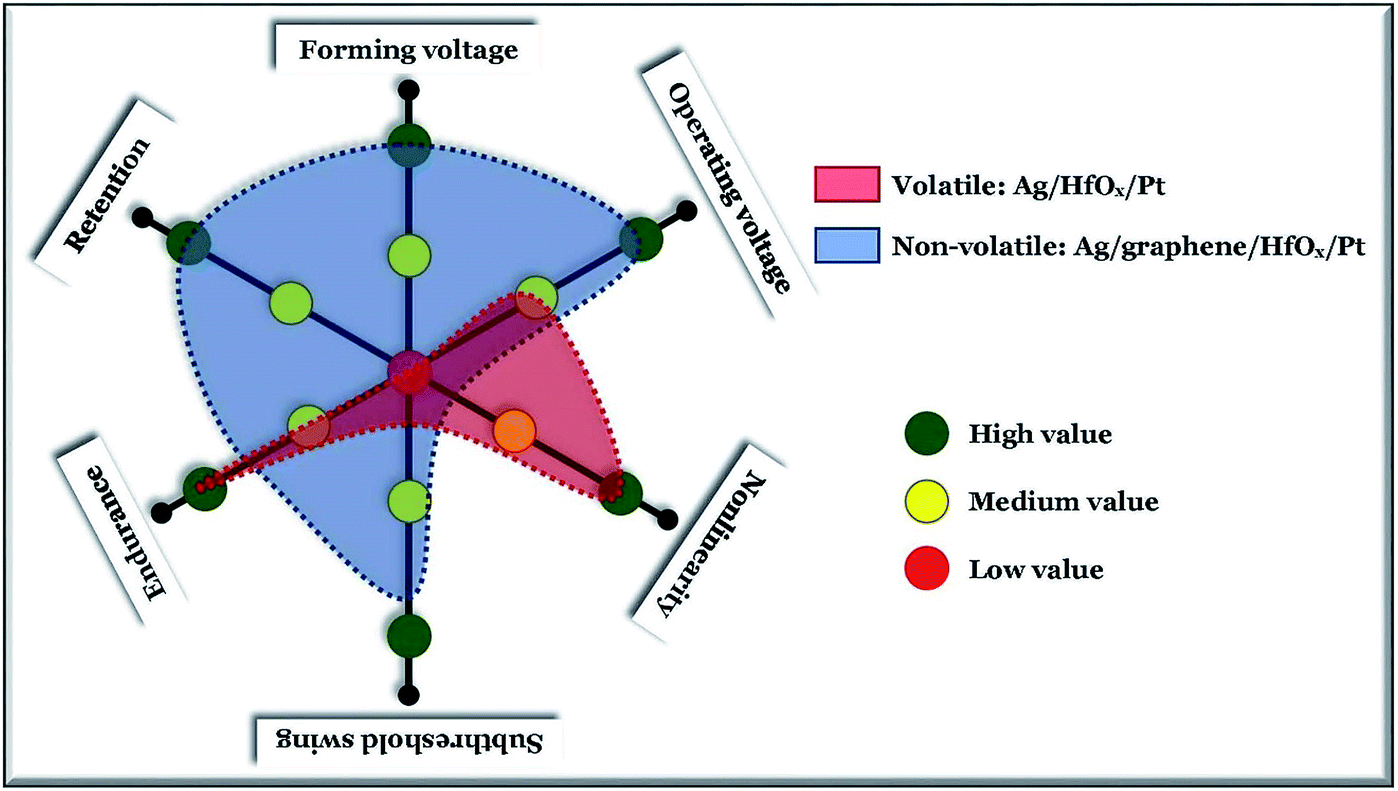 | ||
| Fig. 6 Performance summary. Schematic illustration of the performance summary for with and without graphene based devices. The device without graphene can show volatile switching and the device with graphene-barrier can show nonvolatile switching. | ||
Although device-to-device performance variation is observed, the variation can be improved by improving the graphene film transfer process. Here we must mention that the quality and grain boundaries of the graphene film are playing a major role to define the switching process. The 3 × 3 μm2 devices without and with grain boundaries are shown in the ESI Fig. S2a and c,† respectively. Zoom-in pseudo-colored view of the cross-points show that there is no such grain boundary present in one device (Fig. S2b†) whereas large grains are crossing through the other one (Fig. S2d†). Due to the presence of the larger grain-boundary in the damaged graphene barrier layer, it is easy for the Ag cations to diffuse through the grains under a smaller applied bias condition. The graphene film transfer process can introduce the grains in the graphene film. Depending on the film quality through the device active area, the electrical performance can be changed which is evident in the forming characteristics for defective graphene based devices (ESI Fig. S3†). A poor graphene barrier with lower forming voltage can behave as a TS. In short, the devices with good quality graphene film need a higher forming voltage and can be operated under the MS mode.
Conclusions
In conclusion, we have investigated the graphene interface barrier layer induced transformation of TS behavior into MS in Ag-based RRAM devices. The standard non-graphene Ag-based devices show high quality selector performance with a selectivity >108 and sub-threshold swing of ∼1 mV dec−1. The volatile switching of the non-graphene Ag-based devices changes to a stable nonvolatile one with a graphene barrier layer, by enhancing the forming probability of a stress induced localized conducting filament. In graphene-based devices the MS can be operated below ±1.0 V, with multiple storing ability. However, the grains crossing through devices can degrade the performance which can be further reduces by scaling the device size.Conflicts of interest
There are no conflicts to declare.Acknowledgements
This work was supported by the National Natural Science Foundation of China under Grant No. 61732020, 61851402.References
- M. A. Zidan, J. P. Strachan and W. D. Lu, Nat. Electron., 2018, 1, 22 CrossRef.
- W. Banerjee, Q. Liu, S. Long, H. Lv and M. Liu, J. Phys. D: Appl. Phys., 2017, 50, 303002 CrossRef.
- J. J. Yang, M. D. Pickett, X. Li, D. A. Ohlberg, D. R. Stewart and R. S. Williams, Nat. Nanotechnol., 2008, 3, 429 CrossRef CAS PubMed.
- R. Waser, R. Dittmann, G. Staikov and K. Szot, Adv. Mater., 2009, 21, 2632 CrossRef CAS.
- Z. Wang, M. Rao, R. Midya, S. Joshi, H. Jiang, P. Lin, W. Song, S. Asapu, Y. Zhuo and C. Li, Adv. Funct. Mater., 2018, 28, 1704862 CrossRef.
- H. Sun, Q. Liu, C. Li, S. Long, H. Lv, C. Bi, Z. Huo, L. Li and M. Liu, Adv. Funct. Mater., 2014, 24, 5679 CrossRef CAS.
- Z. Wang, S. Joshi, S. E. Savel’ev, H. Jiang, R. Midya, P. Lin, M. Hu, N. Ge, J. P. Strachan and Z. Li, Nat. Mater., 2017, 16, 101 CrossRef CAS.
- C.-P. Hsiung, H. W. Liao, J. Y. Gan, T. B. Wu, J. C. Hwang, F. Chen and M. J. Tsai, ACS Nano, 2010, 4, 5414 CrossRef CAS PubMed.
- G. Du, C. Wang, H. Li, Q. Mao and Z. Ji, AIP Adv., 2016, 6, 085316 CrossRef.
- B. K. You, J. M. Kim, D. J. Joe, K. Yang, Y. Shin, Y. S. Jung and K. J. Lee, ACS Nano, 2016, 10, 9478 CrossRef CAS PubMed.
- S. Liu, N. Lu, X. Zhao, H. Xu, W. Banerjee, H. Lv, S. Long, Q. Li, Q. Liu and M. Liu, Adv. Mater., 2016, 28, 10623 CrossRef CAS PubMed.
- L. Liu, D. Yu, W. Ma, B. Chen, F. Zhang, B. Gao and J. Kang, Jpn. J. Appl. Phys., 2015, 54, 021802 CrossRef.
- I. Valov, I. Sapezanskaia, A. Nayak, T. Tsuruoka, T. Bredow, T. Hasegawa, G. Staikov, M. Aono and R. Waser, Nat. Mater., 2012, 11, 530 CrossRef CAS PubMed.
- J. Yoo, J. Woo, J. Song and H. Hwang, AIP Adv., 2015, 5, 127221 CrossRef.
- X. Zhao, S. Liu, J. Niu, L. Liao, Q. Liu, X. Xiao, H. Lv, S. Long, W. Banerjee, W. Li, S. Si and M. Liu, Small, 2017, 13, 1603948 CrossRef PubMed.
- J. Yoo, J. Park, J. Song, S. Lim and H. Hwang, Appl. Phys. Lett., 2017, 111, 063109 CrossRef.
- U.-B. Han, D. Lee and J.-S. Lee, NPG Asia Mater., 2017, 9, e351 CrossRef CAS.
- J. Wang, F. Ma and M. Sun, RSC Adv., 2017, 7, 16801 RSC.
- Y.-J. Huang and S.-C. Lee, Sci. Rep., 2017, 7, 9679 CrossRef PubMed.
- F. Hui, E. Grustan-Gutierrez, S. Long, Q. Liu, A. K. Ott, A. C. Ferrari and M. Lanza, Adv. Electron. Mater., 2017, 3, 1600195 CrossRef.
- J. S. Bunch, S. S. Verbridge, J. S. Alden, A. M. Van Der Zande, J. M. Parpia, H. G. Craighead and P. L. McEuen, Nano Lett., 2008, 8, 2458 CrossRef CAS PubMed.
- H. Tian, H.-Y. Chen, B. Gao, S. Yu, J. Liang, Y. Yang, D. Xie, J. Kang, T.-L. Ren and Y. Zhang, Nano Lett., 2013, 13, 651 CrossRef CAS PubMed.
- H. Tian, H.-Y. Chen, T.-L. Ren, C. Li, Q.-T. Xue, M. A. Mohammad, C. Wu, Y. Yang and H.-S. P. Wong, Nano Lett., 2014, 14, 3214 CrossRef CAS PubMed.
- W. Banerjee, W. F. Cai, X. Zhao, Q. Liu, H. Lv, S. Long and M. Liu, Nanoscale, 2017, 9, 18908 RSC.
- W. Banerjee, X. Zhang, Q. Luo, H. Lv, Q. Liu, S. Long and M. Liu, Adv. Electron. Mater., 2018, 4(2), 1700561 CrossRef.
- P. Calka, M. Sowinska, T. Bertaud, D. Walczyk, J. Dabrowski, P. Zaumseil, C. Walczyk, A. Gloskovskii, X. Cartoixà, J. Suñé and T. Schroeder, ACS Appl. Mater. Interfaces, 2014, 6, 5056 CrossRef CAS PubMed.
- B. Traoré, P. Blaise, E. Vianello, L. Perniola, B. D. Salvo and Y. Nishi, IEEE Trans. Electron Devices, 2016, 63, 360 Search PubMed.
- W. Banerjee, X. Xu, H. Liu, H. Lv, Q. Liu, H. Sun, S. Long and M. Liu, IEEE Electron Device Lett., 2015, 36(4), 333 CAS.
- W. Banerjee, X. Xu, H. Lv, Q. Liu, S. Long and M. Liu, Adv. Electron. Mater., 2018, 3(12), 1700287 CrossRef.
- R. Midya, Z. Wang, J. Zhang, S. E. Savel’ev, C. Li, M. Rao, M. H. Jang, S. Joshi, H. Jiang, P. Lin, K. Norris, N. Ge, Q. Wu, M. Barnell, Z. Li, H. L. Xin, R. S. Williams, Q. Xia and J. J. Yang, Adv. Mater., 2017, 29, 1604457 CrossRef PubMed.
- Y. Park, U. B. Han, M. K. Kim and J. S. Lee, Adv. Electron. Mater., 2018, 4, 1700521 CrossRef.
- M. Lübben, P. Karakolis, V. Ioannou-Sougleridis, P. Normand, P. Dimitrakis and I. Valov, Adv. Mater., 2015, 27, 6202 CrossRef PubMed.
- M. Lanza, H.-S. P. Wong, E. Pop, D. Ielmini, D. Strukov, B. C. Regan, L. Larcher, M. A. Villena, J. J. Yang, L. Goux, A. Belmonte, Y. Yang, F. M. Puglisi, J. Kang, B. M. Köpe, E. Yalon, A. Kenyon, M. Buckwell, A. Mehonic, A. Shluger, H. Li, T.-H. Hou, B. Hudec, D. Akinwande, R. Ge, S. Ambrogio, J. B. Roldan, E. Miranda, J. Suñe, K. L. Pey, X. Wu, N. Raghavan, E. Wu, W. D. Lu, G. Navarro, W. Zhang, H. Wu, R. Li, A. Holleitner, U. Wurstbauer, M. C. Lemme, M. Liu, S. Long, Q. Liu, H. Lv, A. Padovani, P. Pavan, I. Valov, X. Jing, T. Han, K. Zhu, S. Chen, F. Hui and Y. Shi, Adv. Electron. Mater., 2019, 5, 1800143 CrossRef.
- M. Lanza, Materials, 2014, 7, 2155 CrossRef PubMed.
- Y. Shi, Y. Ji, F. Hui, M. Nafia, M. Porti, G. Bersuker and M. Lanza, Adv. Electron. Mater., 2015, 1, 1400058 CrossRef.
- M. lanza, G. Bersuker, M. Porti, E. Miranda, M. Nafia and X. Aymerich, Appl. Phys. Lett., 2012, 101, 193502 CrossRef.
Footnote |
| † Electronic supplementary information (ESI) available. See DOI: 10.1039/c9na00409b |
| This journal is © The Royal Society of Chemistry 2019 |