
 Open Access Article
 This Open Access Article is licensed under a Creative Commons Attribution-Non Commercial 3.0 Unported Licence
Weaving nanostructures with site-specific ion induced bidirectional bending†
Vivek
Garg
 abc,
Tsengming
Chou
d,
Amelia
Liu
e,
Alex
De Marco
f,
Bhaveshkumar
Kamaliya
acg,
Shi
Qiu
c,
Rakesh G.
Mote
*b and
Jing
Fu
*c
abc,
Tsengming
Chou
d,
Amelia
Liu
e,
Alex
De Marco
f,
Bhaveshkumar
Kamaliya
acg,
Shi
Qiu
c,
Rakesh G.
Mote
*b and
Jing
Fu
*c
aIITB-Monash Research Academy, Indian Institute of Technology Bombay, Powai, Mumbai 400076, India
bDepartment of Mechanical Engineering, Indian Institute of Technology Bombay, Powai, Mumbai 400076, India. E-mail: rakesh.mote@iitb.ac.in
cDepartment of Mechanical and Aerospace Engineering, Monash University, Wellington Road, Clayton, Victoria 3800, Australia. E-mail: jing.fu@monash.edu
dLaboratory of Multiscale Imaging, Stevens Institute of Technology, Hoboken, NJ 07030, USA
eMonash Centre for Electron Microscopy, Monash University, Clayton, VIC 3800, Australia
fDepartment of Biochemistry and Molecular Biology, Monash University, Clayton, VIC 3800, Australia
gDepartment Physics, Indian Institute of Technology Bombay, Powai, Mumbai 400076, India
First published on 20th June 2019
Abstract
Site-specific ion-irradiation is a promising tool fostering strain-engineering of freestanding nanostructures to realize 3D-configurations towards various functionalities. We first develop a novel approach of fabricating freestanding 3D silicon nanostructures by low dose ion-implantation followed by chemical-etching. The fabricated nanostructures can then be deformed bidirectionally by varying the local irradiation of kiloelectronvolt gallium ions. By further tuning the ion-dose and energy, various nanostructure configurations can be realized, thus extending its horizon to new functional 3D-nanostructures. It has been revealed that at higher-energies (∼30 kV), the nanostructures can exhibit two-stage bidirectional-bending in contrast to the bending towards the incident-ions at lower-energies (∼16), implying an effective transfer of kinetic-energy. Computational studies show that the spatial-distribution of implanted-ions, dislocated silicon atoms, has potentially contributed to the local development of stresses. Nanocharacterization confirms the formation of two distinguishable ion-irradiated and un-irradiated regions, while the smoothened morphology of the irradiated-surface suggested that the bending is also coupled with sputtering at higher ion-doses. The bending effects associated with local ion irradiation in contrast to global ion irradiation are presented, with the mechanism elucidated. Finally, weaving of nanostructures is demonstrated through strain-engineering for new nanoscale artefacts such as ultra-long fully-bent nanowires, nano-hooks, and nano-meshes. The aligned growth of bacterial-cells is observed on the fabricated nanowires, and a mesh based “bacterial-trap” for site-specific capture of bacterial cells is demonstrated emphasizing the versatile nature of the current approach.
Introduction
Energetic ion induced irradiation and implantation are used extensively for doping and inducing functionalities in the nanostructures for desired applications.1,2 Nanostructures exhibit unusual transformations under ion induced irradiation, due to the nanostructure dimensions being comparable to the collision cascade in contrast to their bulk counterparts,1 providing extended functionality in the nanotechnology domain. The mesoscopic properties of these nanostructures under ion irradiation, in addition to the quantum size effects, are governed by the surface effects due to their high surface-to-volume ratio. The interplay among the size, shape, and composition of nanostructures, in addition to the ion species used, governs the physical and chemical characteristics. Mechanical properties such as tensile and compressive stresses can be developed in the lattice atoms under ion irradiation, which induces plastic deformation of nanostructures.3–5The ion-induced plastic deformation is considered as a combined effect of ion implantation, defect formation, and vacancy and interstitial generation; and ion irradiation has been demonstrated for tailoring of carbon nanotubes,6 cantilevers,7 semiconductor nanowires (NWs),8 plasmonic nanostructures,9 3D and thin film origami nanostructures,10,11etc. The irradiation and implantation of ions, depending on the balance between the damage formation and annihilation due to thermal spike, recombination rates,12 can produce stresses of the order of several GPa.13 Through a controlled dose of the ion beam, NWs can be aligned in different orientations towards the beam at sufficient ion doses. In addition, surface charging effects during ion irradiation result in electrostatic forces, which induce the bending in the direction opposite to the incident ion beam.14 Ion-induced amorphization and recrystallization is also considered to play an important role during plastic deformation, and bending was demonstrated to occur in the regions which were fully amorphized.15 Other phenomena are known to occur during ion irradiation, such as void induced stress generation, dynamic annealing of ion-induced defects,16 the formation of interstitial clusters beyond the collision cascade,17 and atomic mass transport.18 These effects and plastic deformation rely heavily on the ion beam parameters such as energy, ion mass, ion dose, etc., and target properties such as geometry, composition, crystallinity, temperature, etc. Nanostructures also exhibit improved sputtering and dynamic annealing of defects in contrast to their bulk counterparts. Thus, the ion induced irradiation and manipulation of nanostructures become important to investigate the underlying mechanisms and designing anticipated functionalities.
This work demonstrates a novel method for fabrication of functional 3D nanostructures through (1) wet etching of ion implanted silicon (Si) for freestanding nanostructures and (2) ion induced in situ 3D deformation of the nanostructure. To investigate the fundamental mechanisms, Focused Ion Beam (FIB) equipped with a liquid gallium source was employed for in situ bending of Si nanowires (NWs), which have been fabricated through the proposed combined implantation/wet etching approach. Observation of bidirectional bending of these NWs, i.e. initially bending away and then bending towards the ion beam at an increased ion dose during successive time intervals, inspires controlled weaving and strain engineering of nanostructures for the realization of advanced 3D nanostructures for desired functionalities. The underlying physics and site-specific ion-induced bending mechanism of Si NWs are investigated through both experimental and computational studies, to provide new insights for controlling nanostructures in situ.
Materials and methods
Wet etching of ion implanted silicon
In situ ion induced bending
Suspended Si NWs prepared through implantation followed by wet etching were used for in situ bending experiments in the dual beam FEI Quanta 3D system. The suspended NWs on two contact pads were first cut by an ion beam of 1.5 pA current, to produce freestanding NWs for bending experiments. The NW cutting was carried out using a single pixel width line and beam overlap of 50%. No observable bending occurred under the optimized cutting conditions. Site-specific ion-induced bending was employed irradiating a rectangular pattern of dimensions 0.5 × 0.5 μm2 perpendicular to the NW length i.e. the FIB incidence angle was kept at 90 degrees, unless specified. The rectangular patterns were chosen to be sufficiently larger than the NWs to avoid any misalignment of the ion-beam. The ion dose was varied by controlling the exposure time or several passes, with a constant dwell time of 1 μs, current of 1.5 pA, and beam overlap of 50%. Three acceleration voltages high-30 kV, medium-16 kV, and low-2 kV were employed for the bending experiments.Monte Carlo simulation
Ion-material interactions, including Ga implantation, atomic displacements, and point defect (vacancies and interstitials) formation are simulated to study the ion-induced bending phenomenon. Monte Carlo (MC) simulations were performed with the software package Stopping and Range of Ions in Matter (SRIM)19 based on binary collision approximations. A monolayer with typical values, threshold displacement energy of 15 eV and density of 2.32 g cm−3,20 was employed for a 100 nm thick Si target. MC calculations are performed at high-30 kV, medium-16 kV, and low-2 kV acceleration voltages to illustrate the bending phenomenon.TEM imaging and characterization
Si NW samples for Transmission Electron Microscopy (TEM) were prepared using the FIB lift-out technique using a Kleindiek micromanipulator (Model MM3A-EM) and platinum gas injection system (Pt GIS) equipped with the FIB/SEM system. The NWs fabricated over the Si substrate were first welded to the micromanipulator tip with Pt, and the other end of the NW was then cut with FIB, to lift-out the NW from the substrate. The NWs were subsequently transferred and welded to copper lift-out TEM grids (Ted Pella, product 460-204). Exposure to the ion beam during imaging was kept to a minimum to avoid unintentional damage and bending of the NWs during transfer. The NWs, after transferring to the TEM grid, were exposed to a FIB at two locations to get bent NWs for nanostructural characterization. TEM imaging of the samples was carried out on a FEG-S/TEM (CM20 FEG-S/TEM, Thermo Fisher, USA) operating at 200 kV.Cell sample preparation and trapping
The cell samples were first subcultured from commercial strain ATCC 13883 and 35218 on agar plates as detailed in previous studies.21,22 If fixation is required, the cells were fixed with 2.5% glutaraldehyde in phosphate-buffered saline (PBS) for 1 h. The cell samples were then rinsed three times with distilled water and stored in 4 °C refrigerator. Prior to experiments, the cells in suspension were pipetted to glass slides and confirmed using a light microscope. For cell trapping experiments, a droplet of bacterial cells was then pipetted at 45 degrees to the Si wafer surface with the fabricated traps, and the liquid was removed immediately by blotting with filter paper (Whatman blotting paper).Results and discussion
Si NWs fabricated with FIB implantation and wet chemical etching are utilized for in situ FIB induced bending experiments (see ESI Fig. S1† for NW fabrication). Si NWs suspended on two contact pads are cut with FIB to allow the realization of NWs that are freestanding at one end and clamped to the contact pad at their base to study the bending phenomenon. Fig. 1(a) shows a false-coloured composite image of a Si NW obtained through a series of representative SEM images acquired at successive time-intervals during 30 kV Ga ion-beam irradiation with increasing dose. The ion beam is incident along the vertical direction as indicated through an arrow in Fig. 1(a), and the irradiated sites are away from the NW free end. Initially, the NW starts to bend in the downward direction, i.e. in the direction away from the beam incidence. With the ion dose increased beyond a certain threshold, the NW starts bending in the upward direction. Finally, the NW aligns itself in the vertical direction, i.e. along the direction of beam incidence. The geometry of the bent NW does not change after the ion beam irradiation is stopped; suggesting that the NW underwent plastic deformation in the irradiated region. The bidirectional nature of the bending, induced through the ion beam dose, provides an additional degree of freedom and can be employed for controlled manipulation of nanostructures offering a variety of 3-dimensional (3D) configurations, extending the nanofabrication capabilities of ion beams.23–27 A typical 3D Si mesh structure obtained via nanostructure weaving through ion-induced bidirectional bending is depicted in the SEM image in Fig. 1(b). The bending experienced by the nanostructures during in situ FIB irradiation must be a consequence of the stresses originating from the volume change due to implanted ions, point defects, and defect clusters in the Si lattice from a physical point of view. The development of such stresses in the lattice can generate a net bending moment, which will, in turn, lead to bending of the nanostructures. The location of these developed stresses with respect to the NW neutral axis, in principle, should govern the nanostructure bending direction.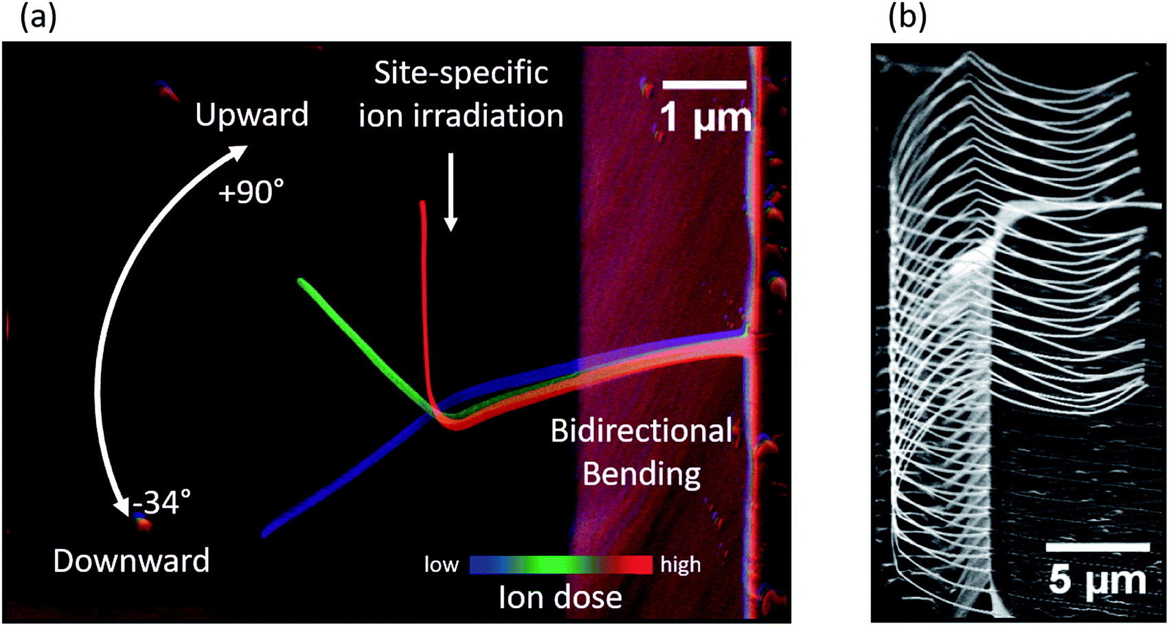 | ||
| Fig. 1 Ion-induced site-specific bidirectional bending: (a) a composite SEM image showing the evolution of a Si NW with increasing ion dose obtained through a series of representative SEM images acquired at successive time-intervals during Ga ion irradiation by a FIB. Initially, the NW bends in the downward direction and eventually aligns towards the incoming Ga ions. (b) SEM image of a typical 3D mesh structure obtained via nanostructure weaving through ion-induced bidirectional bending. | ||
To systematically investigate the effect of ion dose and energies on the bending behaviour of Si nanostructures, Si NWs with a typical diameter of 100–110 nm were employed, which is consistent with the ion implantation range determined in computational studies presented in the next section. A more quantitative analysis of SEM images acquired at successive time-intervals corresponding to each ion beam exposure provides insight and clarification of the bending phenomenon experienced by the nanowire (see Fig. S3 in the ESI† for a series of representative SEM images acquired at successive time-intervals during ion beam irradiation at increasing ion beam doses). In Fig. 2(a), the NW bending angle is plotted as a function of the incident FIB dose (ions per cm2) (a schematic diagram showing the incident FIB on the NW and NW bending angle is included in Fig. S2, ESI†). The negative slope in the plot refers to downward bending, i.e. bending away from the ion beam direction, while the positive slope indicates the bending in the upward direction towards the incident ion beam. Significant bending of Si NWs at ion doses as low as 1014 ions per cm2 is observed. The maximum bending angle in the downward direction is approximately 34 degrees, after which a reversal of the bending direction is observed. With an increased ion dose, the NW aligns itself in the direction parallel to the incident ion beam, i.e. becomes approximately 90 degrees with respect to its initial orientation in the given configuration.
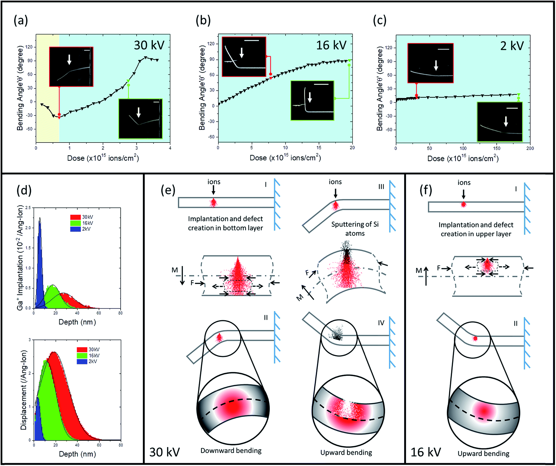 | ||
| Fig. 2 Si nanowires: bending angle plotted as a function of ion dose at (a) 30 kV, two distinct colour regions mark downward and upward bending; (b) 16 kV and (c) 2 kV, with insets showing SEM images of the bent NW (scale bar 1 μm); (d) Ga ion implantation and total atomic displacement distributions/Angstrom-ion caused by Ga ions in the Si substrate at low (2 kV), medium (16 kV), and high (30 kV) acceleration voltages; Schematic illustration of the proposed bending mechanisms: (e) bi-directional bending at 30 kV and (f) upward bending at 16 kV. | ||
In order to further examine the in situ FIB induced bending of Si NWs, ion irradiation at medium (16 kV) and low (2 kV) acceleration voltages, respectively, was carried out (see Fig. S4 in the ESI† for a series of representative SEM images during ion irradiation at successive time intervals with increasing ion dose at 16 kV and 2 kV). The bending angle as a function of ion beam dose is plotted in Fig. 2(b) and (c) at 16 kV and 2 kV, respectively. It can be clearly observed that the formerly straight NW bends towards the incoming ion beam and eventually aligns itself along the beam incidence direction at high ion beam dose. The bending exhibited at 16 kV is in the upward direction only, which is in contrast with the bidirectional bending of the NWs at 30 kV. For a low acceleration voltage of 2 kV, the NW experiences similar upward bending; however, the NWs undergo bending up to a maximum angle of 15° only. The bending rate (i.e. the slope of the bending angle curve plotted with respect to the ion dose) is also affected by the acceleration voltage and the NWs are seen to undergo bending at a slower rate at the lower acceleration voltages.
The NWs, in the current study, were irradiated with an ion-beam incident at 90 degrees to the length of the NWs, to avoid any exposure to the Si substrate. It should be noted that the NW bending demonstrated in the current work is unlikely to be due to the substrate charging phenomenon as reported earlier.14 In addition, the NWs employed in the current experiments are freestanding and away from the Si substrate, which further lowers any possibility of substrate charging. The electrostatic charges induced between the ion-beam and the NW (if assumed to be charged due to the previous beam scan) would be negligible due to a significantly small current (1.5 pA) and ions used for bending. This implies that the bending behaviour observed in our case is not determined by electrostatic forces between the ion beam and the NW.
Our findings of bidirectional bending are in contrast to previous studies on carbon cantilevers,7 nanoporous gold (Au) cantilevers,28,29 and Si NWs;30 where the bending towards incident ion beam was observed irrespective of ion beam energies/target thickness. In addition, the bending exhibited at lower ion energies, observed in the current work, is also in contrast to the bending observations at high ion energies. Thus, there must be additional effects, which lead to the alternate bending behaviour exhibited by the NWs at 30 kV in contrast to the upward bending at 16 kV and needs to be investigated. Moreover, the ion hammering effect for the origin of stresses, similar to the heavy ion irradiation in amorphous materials,3,4 cannot be responsible for NW bending due to the positive thermal coefficient of Si. Similar to the calculations on germanium (Ge) NWs,31 Si would require a negative thermal coefficient of expansion. In addition, an anomalous plastic deformation of Si NWs observed with low energy Ar ions32 reveals that the viscoelastic model for swift heavy ion irradiation,33 to explain the plastic flow of amorphous solids on the basis of a thermal spike region of cylindrical shape formed along the ion beam path, is rather contentious, and the model based on electronic energy loss cannot be generalized to low energy irradiation.
To investigate the underlying physics and the mechanisms involved in the ion induced bidirectional bending, the interaction of energetic Ga ions with Si NWs is evaluated. For the low kV beam energies, the implantation and the defect formation are limited to the few tens of nanometres, while increasing the beam energy results in deeper implantation along the target thickness. The collision cascade is largest for 30 kV and approximately spans 60–65 nm across the target depth, while 16 kV and 2 kV Ga ions are found to create a collision cascade within ∼40 nm and ∼15 nm of the NW thickness respectively (see Fig. S5 in the ESI† for details). These values are based on the consideration of an amorphous Si target in the MC calculations. Fig. 2(d) shows the Ga ion distribution and atomic displacements/Angstrom-ions (a sum of vacancies and replacement collisions) in Si caused by Ga ions calculated using MC simulations. Approximately 742, 420, and 65 vacancies and interstitial pairs are created at 30 kV, 16 kV, and 2 kV, respectively, per implanted Ga ion. The vacancy defects in the collision cascade can be ripened into voids, with the concurrent densification due to interstitial knock-ons.34 The distribution of a cascade along the target depth, due to low and high ion energies, can be used to locate the domains of vacancies or interstitial concentrations. The excess of vacancies is found towards the ion-irradiated surface while the interstitials dominate the un-irradiated surface (see Fig. S5 in the ESI† for details). The volume expansion due to the incorporation of interstitials in the lattice corresponds to the generation of compressive stresses,8 and such lattice strains extend far beyond the collision cascade.35 The excess of vacancies, on the other hand, corresponds to the generation of tensile stresses associated with a contraction of volume. The generation of such stresses is believed to be the primary reason for ion irradiation induced bending.5,7,8,36,37 The volume expansion or swelling around the interstitial is more than the volume contraction around vacancies;38 thus, the formation and location of interstitial clusters play a major role in ion induced bending.39 The formation of such interstitial clusters grows with a prolonged ion exposure followed by sputtering of Si at higher ion doses and reconstruction. The observation of interstitials in the form of dislocation networks through X-ray diffraction imaging of ion irradiated Au nanocrystal support the dominance of interstitials at high ion doses.35 However, at low ion doses, the microstructure is dominated by vacancies.35 It must be noted that the sputtering rates of nanostructures are higher due to their large surface-to-volume ratio,32 when compared with sputtering of their bulk counterparts. At very low ion doses, it is hardly possible to remove surface atoms from Si NWs with Ga ions due to limited sputtering yield of Si.
In addition to the creation of interstitials/vacancies, the collision cascade due to ion irradiation, accompanied by a thermal spike region, develops an atomic mass transport in the region well beyond the implantation range. Such mass transport has been reported for Si nanopore formation with FIB.40 In fact, the direction of atomic mass transport via plastic deformation based on the incident ion energy was understood to be the primary factor controlling the deflection of Al cantilevers through molecular dynamics (MD) simulations.18 Similar observations were made for ion induced bending of Al cantilevers,17 suggesting the bending due to the transport of interstitial clusters far above the irradiated region. An extended dislocation network observed through X-ray diffraction measurements in ion implanted Au nanocrystals further confirms the generation of lattice strains far beyond the ion-damaged layer.35 Such dislocation clusters, extending well beyond the ion implantation range are most likely expected to be of interstitial type.41 Similar formation of dislocation loops in ion irradiated Al has also been observed through TEM imaging.42 The accumulation of interstitial clusters leads to volume expansion in the region beyond the ion implantation range, causing ion induced bending of Al, Au cantilevers.17,29 Low energy ion dosage induces penetration of ions only near the ion-irradiated top region, thereby contributing to the mass transport to the ion-irradiated top region and resulting in upward deflection towards incident ions. High energy ion dosage, on the other hand, induces ion penetration near to the bottom of the ion-irradiated surface (depending on the thickness), and thus providing the mass transport towards the bottom surface, resulting in downward deflection away from the incident ion beam. The compressive stresses are built up in the NW in the ion-irradiated region due to the sputtering of Si atoms from top layers and redistribution of the disturbed atoms in the collision cascade, because of further exposure to ions. The formation of such compressive stresses in the NW surface towards the incident ion beam generates a net bending moment in the upward direction. The NWs, thus, reverses its motion and bends towards the incident ion beam until a new equilibrium state is obtained.
In the current work, we report NWs bending away from the incident ions up to a threshold ion dose of ∼7 × 10¹⁴ ions per cm2 at high energy (Fig. 2(a)). This is due to the volume expansion towards un-irradiated side (bottom) of the NW. However, in earlier studies on GaAs,8 ZnO,36 and Ge NWs,43 the bending of nanostructures away from the incident ions was attributed to the volume expansion in the irradiated side of NWs at shallower depths (low energy irradiation). The alignment towards incident ions was observed during high energy irradiation causing volume expansion towards the un-irradiated side.8,36,43 Such an anomaly is also observed at low energy irradiation in the current work, where the shallower irradiation induced volume expansion towards the irradiated side (NW top) developing upward bending of the Si NWs (Fig. 2(b)).
We further experimented ion irradiation at 30 kV on a Si NW along its entire length (global ion irradiation) similar to the broad/plasma ion irradiation of the NWs/cantilevers reported earlier. This contrasts with the site-specific/local ion irradiation used in this work (Fig. 2). The globally irradiated Si NW, still leading to the volume expansion at 30 kV towards un-irradiated side, was now found to bend upwards/towards incident ions (see Fig. S7 in the ESI† for details). No bidirectional bending was observed. This is similar to the earlier reported bending of the NWs towards the ion beam if the volume expansion is towards the un-irradiated side of the NWs.8,36,43 In fact, local irradiation with shallow penetrations, limited to the irradiation side of Si NWs30 and carbon cantilevers7 cause the nanostructure to bend towards the incident ions. This highlights the strong influence of the choice of the irradiation scheme, whether site-specific/local or global, on the bending behaviour of NWs, in addition to the other factors like collision cascade, associated volume changes, mass transport, sputtering, etc.
These findings, suggesting the importance of sites being irradiated, i.e. localized or global, are crucial, and provide additional control for weaving of nanostructures in addition to the ion beam parameters. Such bending effects can potentially arise from the density difference between the damaged and un-damaged regions.39 For local irradiation, the volume expansion in the irradiated domain is surrounded by the un-damaged region leading to such density difference and can be a probable cause for the observed bending effects of localized ion irradiation (refer to Fig. S8 in the ESI† for summary and comparison of mechanisms for local vs. global ion irradiation induced bending). The volume expansion develops reactive forces in the un-damaged region. Such forces lead to the generation of a bending moment on the NWs, the direction of which depends on the relative location of volume expansion region.
In light of the above discussion, the bending mechanism is presented schematically in Fig. 2(e) and (f) for ion induced NW bending at high and low ion energies, respectively. The volume expansion, caused at high ion energies towards the NW un-irradiated side, surrounded by the un-damaged region, develops a force towards the region of volume expansion. The development of such force towards the NW un-irradiated side leads to the generation of a downward bending moment, as shown through the schematics in Fig. 2(e): I and II, and the NW undergoes a downward bending. The phenomena of sputtering and surface reconstruction starts dominating at higher energies with a continued exposure to the ion beam i.e. at a high dose (Fig. 2(e): III and IV), which is evident from the NW at the onset of bending reversal (SEM image Fig. S3(d) in the ESI†). The removal of atoms at high energies (30 kV), leads to the reversal of the bending moment and the NW bends in the reverse direction. In this stage, the NW bending behaviour is dominated by the sputtering of the irradiated region, and a faster bending towards incident ion beam is observed (also evident from a steep slope of the bending curve during the upwards bending as seen from Fig. 2(a)). For low ion energies, on the other hand, the collision cascade and interstitials including the implanted ions occur towards the ion-irradiated side of the NW (Fig. 2(f): I–II). This creates a volume expansion in the NW ion-irradiated top region, and NW undergoes upward bending at low energies and continues aligning itself towards the ion beam direction at successive ion irradiation.
In order to further consolidate the bending mechanism, nanostructural investigations based on TEM were carried out on Si NWs in order to study the ion-induced deformations (see Fig. S6 is ESI† for details on TEM sample preparation). The TEM images of a fabricated Si NW with diameter ∼110 nm are shown in Fig. 3(a) and (b). The contrast in the high-magnification TEM image as shown in Fig. 3(b), and the associated electron diffraction pattern as shown in Fig. 3(c), both indicate the polycrystalline nature of fabricated NWs. The polycrystalline transformation of Si NWs is believed to be due to ion beam implantation during the fabrication process to obtain the suspended Si NWs. The Si NW was bent with FIB irradiation at an acceleration voltage of 30 kV, and the corresponding TEM characterization results are included in Fig. 3(d)–(h). The NW, even after bending, is found to maintain the polycrystalline state as evident from the electron diffraction pattern in the Fig. 3(f). A high-magnification TEM image of the bent NW is included in Fig. 3(e). Upon prolonged exposure (high dose) to Ga ion irradiation, the NW exhibits two clearly distinguishable regions: sparse, ion-irradiated top region (Region (1)) and un-irradiated, bottom region (Region (2)). The sparse ion-irradiated region (Region (1)) in Fig. 3(e) and (g) is in contrast to the un-irradiated region in Fig. 3(b) and (h) visibly evident from the image contrast. The NW irradiated surface, as evident from the high magnification TEM images in Fig. 3(e) and (g) exhibiting a smoothened irradiated surface, indicates the ion beam sputtering effects associated during the bending process at high ion doses. The irradiated NW surface, in contrast to the un-irradiated surface, appears to have reduced surface roughness. The power spectral density (PSD) calculations are carried out for analysing and comparing the surface roughness of irradiated and un-irradiated NW surfaces as shown in Fig. 3(i), with a TEM image in the inset showing the outline of compared surfaces. The un-irradiated NW surface has both low frequency and high-frequency roughness towards the higher side as compared to the ion-irradiated NW surface. The improvement in the surface roughness of the ion-irradiated NW surface is an indication of ion-induced smoothening process. Thus, the nanostructural characterization of the bent NW at higher doses confirms that the bending behaviour is dominated by sputtering of the NW atoms at the irradiated surface, and the NW bends towards the incident ion beam.
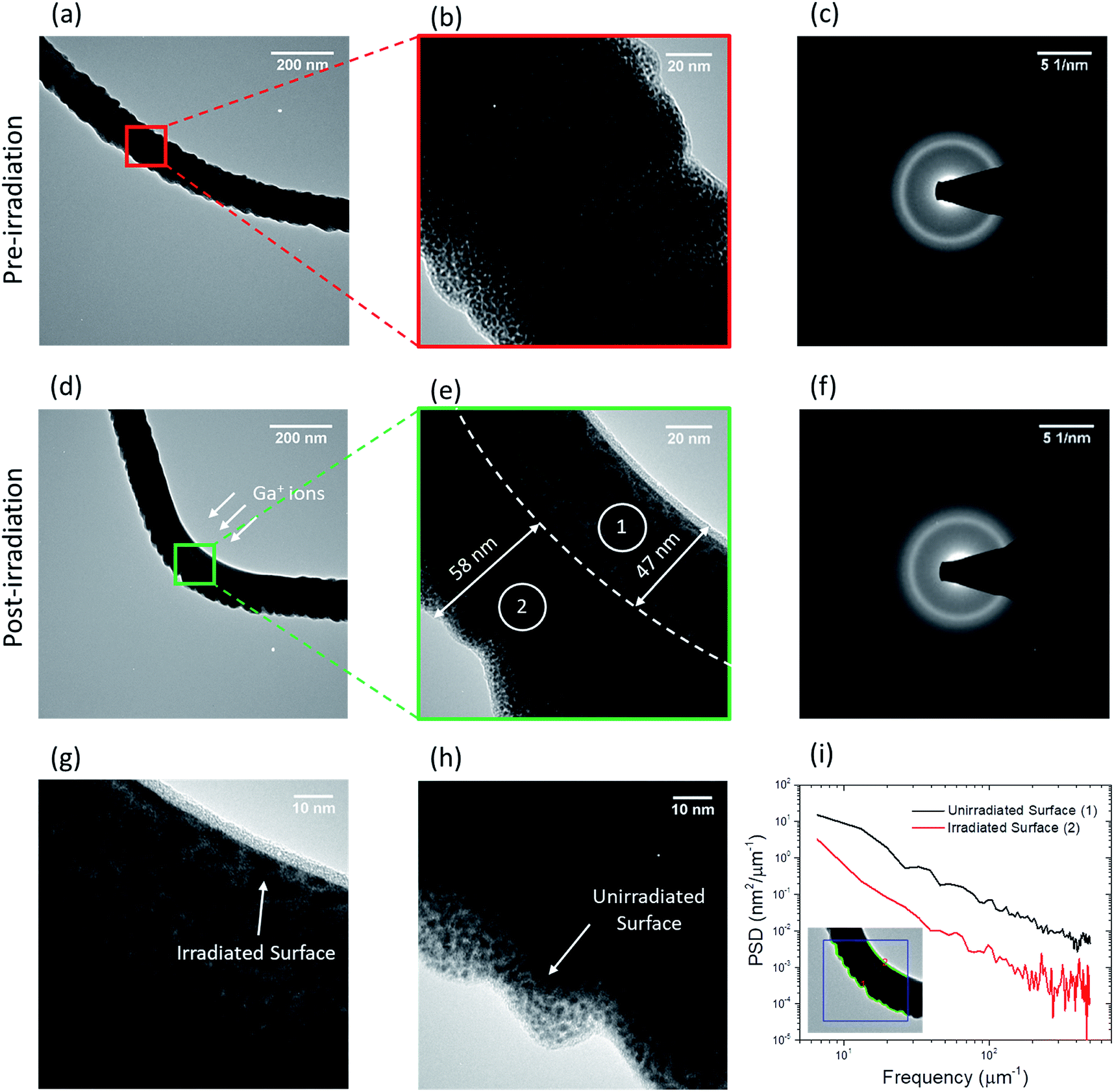 | ||
| Fig. 3 Nanostructural characterization of Ga ion irradiated Si nanowires (NWs): Transmission Electron Microscope (TEM) image showing (a) a fabricated, un-irradiated Si NW, (b) a magnified TEM image of the NW, and (c) diffraction pattern from the NW; (d) Si NW after in situ ion induced bending, (e) magnified TEM image of bent NW, and (f) diffraction pattern from the ion-irradiated NW. (g) and (h) show further magnified TEM images of ion-irradiated and un-irradiated surface, respectively; (i) power spectral density function against the spatial frequency of the surface roughness for un-irradiated and irradiated surface. | ||
Weaving 3D nanostructures
In situ FIB induced bidirectional bending demonstrated here can be employed for controlled manipulation and weaving of freestanding nanostructures into complex 3-dimensional nanostructures for desired functionality. The main limitation for the realization of such 3-dimensional nanostructures, however, is the fabrication of freestanding nanostructures. The residual stresses developed during thin film deposition and fabrication of such freestanding nanostructures can lead to unwanted and uncontrolled deformations. The fabrication of suspended nanostructures through the combination of FIB implantation and bulk structuration via wet etching of Si in this work overcomes such issues. Controlled manipulation and weaving of fabricated suspended nanostructures were further carried out with FIB in situ to realize 3D nanostructures. Fig. 4 shows SEM images of 3D nanostructures obtained via controlled weaving and nanostructure manipulation. We would like to point out the effects of sputtering during controlled manipulation and weaving of nanostructures. As discussed earlier, the continued exposure to the ion beam leads to the sputtering of the nanostructures and reversal of bending at high ion energies. For the controlled manipulation and weaving of nanostructures towards the ion beam at 30 kV, we observed the thinning of the bending cross-section, arising from the sputtering of Si with an ion beam dose of ∼7 × 10¹⁴ ions per cm2 at 30 kV. The sputtering effects associated with ion induced bending during nanomanipulation could be a limiting aspect for geometry sensitive applications. Such sputtering effects, however, can be avoided employing low ion doses with high/low ion energies to induce downward/upward bending, respectively. | ||
| Fig. 4 Controlled weaving and nanostructure manipulation. SEM image (false-coloured) of (a) an ultra-long fully bent NW with normal incident ion beam irradiation on the NW; (b) NWs bent in two alternative directions with three subsequent FIB irradiations in the direction normal to NWs; (c) an array of NWs bent in the downward direction; (d) a hook-shaped 3D nanostructure fabricated through FIB irradiation repeated multiple times along the NW; (e) 3D folded nanostructures in the form of a mesh; (f) SEM image of suspended NWs for live cell imaging; (g) corresponding optical microscopic image showing the bacteria loaded nanowires with the inset showing the SEM image of the cell showing aligned growth on the NWs; (h) conceptual design and SEM image of a “bacterial mesh trap” fabricated via bending of the suspended Si mesh; (i) SEM image (false-coloured) of the prototype “bacterial mesh trap” after capturing the bacterial cells. | ||
An ultra-long vertical NW (length 33 μm and high aspect ratio of 300) was obtained via ion beam induced upward bending of a Si NW freestanding at one end and attached to the Si post at the other end. The ultra-long fully bent NW is shown in Fig. 4(a), which has been bent at 90 degrees. Such high aspect ratio NWs can be utilized for multifunctional applications in photonics or materials sciences. A pair of NWs bent in two alternative perpendicular directions is shown in Fig. 4(b), where the ion beam was irradiated at three locations along the NW length and in the directions perpendicular to the previous scan. The NWs bent in two alternative perpendicular directions were obtained through ion beam irradiation along the NW length at multiple locations. The ion beam was incident perpendicular in subsequent location to the direction in the previous location along the NW length to realize the NWs bent in two perpendicular directions. An array of suspended NWs bent in the downward direction, i.e. in the direction opposite to the incident ion beam, is shown in Fig. 4(c). Such in situ bidirectional manipulations demonstrate the ease with which the nanostructures can be designed for desired functionality.
A hook-shaped nanostructure, fabricated through multiple FIB irradiations along the NW length, is shown in Fig. 4(d). The hook-shaped nanostructure was fabricated via continuous and controlled bending on a Si NW along its length. The NW was irradiated with Ga ions through a line pattern scan, which was moved along the NW length after each irradiation, resulting in continuous bending of NW and formation of a hook shape. This strategy can be further employed for fabrication of exotic 3-dimensional coil nanostructures through continuous and controlled manipulations along the NW length. The controlled weaving of freely suspended Si mesh nanostructures was further employed through in situ ion irradiation of Si nanostructures in order to realize folded 3D nanostructures. The ion beam was scanned over a pre-defined line pattern on a Si mesh in order to bend it (see Fig. S9 in the ESI† for fabrication details). Fig. 4(e) includes the SEM image of a 3D nanostructure in the form of a mesh, demonstrating the process capability. The analysis of ion induced bending at different processing parameters can be used to ascertain the deterministic nature of the bending process as needed for 3D freeform fabrication. Fig. 2(a)–(c) provide an accurate estimate of processing parameters for realizing the controlled bending of nanostructures. For example, referring to Fig. 2(a), for a nanostructure close to 100 nm in diameter to bend 30 degrees in the downwards direction, an ion dose of ∼5 × 10¹⁴ ions per cm2 at 30 kV should be used. Similarly, for a nanostructure with a bending angle of 30 degrees in the upward direction, an ion dose of ∼2.5 × 10¹⁵ ions per cm2 at 30 kV or ∼4 × 10¹⁵ ions per cm2 at 16 kV should be used.
Thus, the availability of these processing parameters as a reference can be used for deterministic bending of nanostructures for controlled manipulation, as has also been shown through the examples in Fig. 4. This suggests that complex nanostructures can be engineered in situ through ion-induced bending. Thus, the developed approach is effective for fabrication of thin film 3D nanostructures for desired functionalities and will enable the development of future novel nanoscale devices.
The developed approach provides an excellent route for novel single cell applications such as the interactions between bacteria and the Si nanostructures. Bacteria are social organisms, displaying distinct group behaviours, which are often required in large numbers to conduct mechanistic studies for probing the molecular processes for antibiotic resistance, etc.44 Live cell imaging application of the fabricated suspended nanostructures (NWs) is illustrated in Fig. 4(g), where an optical image is shown demonstrating the stained live bacterial cells showing aligned patterns. The corresponding array of suspended NWs used for live cell imaging is shown through the SEM image in Fig. 4(f). The SEM image of bacteria loaded nanowires included in the inset of Fig. 4(g) shows aligned growth similar to the self-assembly and adhesion of the bacterial cell over vertical NWs demonstrated previously.45,46 The proposed approach in the study provides a simpler yet more flexible alternative towards the study and understanding of cell adhesion with 3D nanostructures. A new “bacterial mesh trap” is designed through the developed nanofabrication and the in situ FIB manipulation approach for capturing the bacterial cells. Fig. 4(h) presents the design of the trap and the obtained structures via fabrication and controlled manipulation of the Si suspended mesh (see Fig. S10 in the ESI† for fabrication details). The fabricated “bacterial mesh trap” is demonstrated to be effective for capturing of bacterial cells in solution as shown in Fig. 4(i). The mesh size (∼1 μm) ensured bacteria capturing within the trap, while being permeable to nutrients and waste products through the mesh. The vertical mesh sides further wrapped the bacteria as enclosing walls, facilitating three-dimensional organization, which has been infeasible previously.
Conclusions
In this work, novel fabrication of Si 3D nanostructures is demonstrated through a combination of ion implantation and wet etching of Si followed by keV ion induced in situ controlled manipulation. The achievements include (1) suspended Si NWs fabricated through the combination of FIB implantation followed by top-down bulk structuration via anisotropic wet etching of Si. (2) One notable finding is the bidirectional bending at higher (∼30 kV) ion energies. The Si NWs were found to bend away from an incident ion beam initially possibly due to penetration of the incident Ga ions and the resulting formation of defects. The NWs eventually align in the direction of the incoming ion beam due to the removal of atoms from the Si lattice possibly from sputtering effects. Unlike irradiation at 30 kV, the NWs only exhibited bending towards incident ions at lower ion energies (including 2 kV and 16 kV). We further observed that the bending rate of Si NWs is dependent on ion energies, and it was found to decrease with lowering ion energies. An important consideration of local vs. global ion irradiation correlating the bending effects associated with local ion irradiation in contrast to global ion irradiation is presented. (3) The bidirectional nature of ion-induced bending provides an additional degree of freedom, and the proposed method can be utilized for deterministic 3D nanofabrication and manipulation of nanostructures for desired functionalities, such as ultra-long NWs, folded nanomeshes, live cell imaging, and “bacterial mesh traps”. This work will be inspiring for 3D nanofabrication of unique geometries, and open new avenues in the diverse field of ion beams and applications beyond materials science for realization of future nanoscale devices.Conflicts of interest
There are no conflicts to declare.Acknowledgements
The work was financially supported by IITB-Monash Research Academy, the Australian Research Council (DP180103955), and IRCC (Seed grant: Spons/ME/I14079-1/2014), IIT Bombay. Vivek Garg was supported by the Tata Consultancy Services (TCS) research scholarship program. The authors acknowledge the use of facilities within the Monash Centre for Electron Microscopy (MCEM), Monash Campus Cluster (MCC), and Melbourne Centre for Nanofabrication (MCN), Victorian Node of the Australian National Fabrication Facility (ANFF).References
- A. Johannes, H. Holland-Moritz and C. Ronning, Semicond. Sci. Technol., 2015, 30, 033001 CrossRef.
- L. Ma, Y. Tan, M. Ghorbani-Asl, R. Boettger, S. Kretschmer, S. Zhou, Z. Huang, A. V. Krasheninnikov and F. Chen, Nanoscale, 2017, 9, 11027–11034 RSC.
- S. Klaumünzer, C. Li, S. Löffler, M. Rammensee, G. Schumacher and H. C. Neitzert, Radiat. Eff. Defects Solids, 1989, 108, 131–135 CrossRef.
- A. Hedler, S. L. Klaumünzer and W. Wesch, Nat. Mater., 2004, 3, 804–809 CrossRef CAS PubMed.
- T. Yoshida, A. Baba and T. Asano, Jpn. J. Appl. Phys., 2005, 44, 5744 CrossRef CAS.
- B. C. Park, K. Y. Jung, W. Y. Song, B.-h. O and S. J. Ahn, Adv. Mater., 2005, 18, 95–98 CrossRef.
- S. K. Tripathi, N. Shukla, S. Dhamodaran and V. N. Kulkarni, Nanotechnology, 2008, 19, 205302 CrossRef PubMed.
- C. Borschel, R. Niepelt, S. Geburt, C. Gutsche, I. Regolin, W. Prost, F.-J. Tegude, D. Stichtenoth, D. Schwen and C. Ronning, Small, 2009, 5, 2576–2580 CrossRef CAS PubMed.
- A. Cui, Z. Liu, J. Li, T. H. Shen, X. Xia, Z. Li, Z. Gong, H. Li, B. Wang, J. Li, H. Yang, W. Li and C. Gu, Light: Sci. Appl., 2015, 4, e308 CrossRef CAS.
- C. Khattiya, C. Nikolai, H. Jiang, L. Jian, P. Babak and G. S. Paraoanu, Adv. Mater., 2012, 25, 91–95 Search PubMed.
- Z. Liu, H. Du, J. Li, L. Lu, Z.-Y. Li and N. X. Fang, Sci. Adv., 2018, 4, eaat4436 CrossRef PubMed.
- L. Pelaz, L. A. Marqués and J. Barbolla, J. Appl. Phys., 2004, 96, 5947–5976 CrossRef CAS.
- Y. Ishii, C. S. Madi, M. J. Aziz and E. Chason, J. Mater. Res., 2014, 29, 2942–2948 CrossRef CAS.
- A. Cui, J. C. Fenton, W. Li, T. H. Shen, Z. Liu, Q. Luo and C. Gu, Appl. Phys. Lett., 2013, 102, 213112 CrossRef.
- E. F. Pecora, A. Irrera, S. Boninelli, L. Romano, C. Spinella and F. Priolo, Appl. Phys. A: Mater. Sci. Process., 2011, 102, 13–19 CrossRef CAS.
- N. S. Rajput, Z. Tong and X. Luo, Mater. Res. Express, 2015, 2, 015002 CrossRef.
- D. R. Gomes, A. A. Turkin, D. I. Vainchtein and J. Th. M. De Hosson, J. Mater. Sci., 2018, 53, 7822–7833 CrossRef CAS.
- C.-L. Wu, F.-C. Li, C.-W. Pao and D. J. Srolovitz, Nano Lett., 2017, 17, 249–254 CrossRef CAS PubMed.
- J. F. Ziegler, M. D. Ziegler and J. P. Biersack, Nucl. Instrum. Methods Phys. Res., Sect. B, 2010, 268, 1818–1823 CrossRef CAS.
- J. W. Corbett and G. D. Watkins, Phys. Rev., 1965, 138, A555–A560 CrossRef.
- B. Liu, M. H. Uddin, T. W. Ng, D. L. Paterson, T. Velkov, J. Li and J. Fu, Nanotechnology, 2014, 25, 415101 CrossRef PubMed.
- J. Li, C. Zheng, B. Liu, T. Chou, Y. Kim, S. Qiu, J. Li, W. Yan and J. Fu, Nanotechnology, 2018, 29, 365705 CrossRef PubMed.
- V. Garg, R. G. Mote and J. Fu, Adv. Mater. Technol., 2018, 3, 1800100 CrossRef.
- V. Garg, R. G. Mote and J. Fu, Opt. Mater., 2019, 94, 75–85 CrossRef.
- V. Garg, R. G. Mote and J. Fu, Microsc. Microanal., 2018, 24, 856–857 CrossRef.
- V. Garg, R. G. Mote and J. Fu, in Precision Product-Process Design and Optimization, Springer, Singapore, 2018, pp. 189–209 Search PubMed.
- V. Garg, R. G. Mote and J. Fu, in 2017 IEEE 17th International Conference on Nanotechnology (IEEE-NANO), 2017, pp. 707–712 Search PubMed.
- S. Punzhin, E. Detsi, A. Kuzmin and J. T. M. D. Hosson, J. Mater. Sci., 2014, 49, 5598–5605 CrossRef CAS.
- D. R. Gomes, A. A. Turkin, D. I. Vainchtein and J. Th. M. De Hosson, Appl. Surf. Sci., 2018, 446, 151–159 CrossRef CAS.
- K. Jun, J. Joo and J. M. Jacobson, J. Vac. Sci. Technol., B: Nanotechnol. Microelectron.: Mater., Process., Meas., Phenom., 2009, 27, 3043–3047 CrossRef CAS.
- L. Romano, N. G. Rudawski, M. R. Holzworth, K. S. Jones, S. G. Choi and S. T. Picraux, J. Appl. Phys., 2009, 106, 114316 CrossRef.
- A. Johannes, S. Noack, W. Wesch, M. Glaser, A. Lugstein and C. Ronning, Nano Lett., 2015, 15, 3800–3807 CrossRef CAS PubMed.
- H. Trinkaus and A. I. Ryazanov, Phys. Rev. Lett., 1995, 74, 5072–5075 CrossRef CAS PubMed.
- J. S. Williams, M. J. Conway, B. C. Williams and J. Wong-Leung, Appl. Phys. Lett., 2001, 78, 2867–2869 CrossRef CAS.
- F. Hofmann, E. Tarleton, R. J. Harder, N. W. Phillips, P.-W. Ma, J. N. Clark, I. K. Robinson, B. Abbey, W. Liu and C. E. Beck, Sci. Rep., 2017, 7, 45993 CrossRef CAS PubMed.
- C. Borschel, S. Spindler, D. Lerose, A. Bochmann, S. H. Christiansen, S. Nietzsche, M. Oertel and C. Ronning, Nanotechnology, 2011, 22, 185307 CrossRef PubMed.
- W. J. Arora, S. Sijbrandij, L. Stern, J. Notte, H. I. Smith and G. Barbastathis, J. Vac. Sci. Technol., B: Nanotechnol. Microelectron.: Mater., Process., Meas., Phenom., 2007, 25, 2184–2187 CrossRef CAS.
- M. Tang, L. Colombo, J. Zhu and T. Diaz de la Rubia, Phys. Rev. B: Condens. Matter Mater. Phys., 1997, 55, 14279–14289 CrossRef CAS.
- O. Camara, I. Hanif, M. Tunes, R. Harrison, G. Greaves, S. Donnelly and J. Hinks, Adv. Mater. Interfaces, 2018, 5, 1800276 CrossRef.
- K. Das, J. B. Freund and H. T. Johnson, J. Appl. Phys., 2015, 117, 085304 CrossRef.
- H. Idrissi, S. Turner, M. Mitsuhara, B. Wang, S. Hata, M. Coulombier, J.-P. Raskin, T. Pardoen, G. V. Tendeloo and D. Schryvers, Microsc. Microanal., 2011, 17, 983–990 CrossRef CAS PubMed.
- S. Lee, J. Jeong, Y. Kim, S. M. Han, D. Kiener and S. H. Oh, Acta Mater., 2016, 110, 283–294 CrossRef CAS.
- I. Hanif, O. Camara, M. A. Tunes, R. W. Harrison, G. Greaves, S. E. Donnelly and J. A. Hinks, Nanotechnology, 2018, 29, 335701 CrossRef PubMed.
- J. L. Connell, A. K. Wessel, M. R. Parsek, A. D. Ellington, M. Whiteley and J. B. Shear, mBio, 2010, 1, e00202–e00210 CrossRef PubMed.
- K. K. Sakimoto, C. Liu, J. Lim and P. Yang, Nano Lett., 2014, 14, 5471–5476 CrossRef CAS PubMed.
- P. K. Sahoo, R. Janissen, M. P. Monteiro, A. Cavalli, D. M. Murillo, M. V. Merfa, C. L. Cesar, H. F. Carvalho, A. A. de Souza, E. P. A. M. Bakkers and M. A. Cotta, Nano Lett., 2016, 16, 4656–4664 CrossRef CAS PubMed.
Footnote |
| † Electronic supplementary information (ESI) available: Si NW fabrication, the bending schematic, detailed bending experiments, Monte Carlo simulations, Si NW TEM sample preparation, global ion irradiation experiments, the bending mechanism: local vs. global ion irradiation, weaving of nanostructures, and bacteria lobster trap fabrication. See DOI: 10.1039/c9na00382g |
| This journal is © The Royal Society of Chemistry 2019 |