
 Open Access Article
 This Open Access Article is licensed under a Creative Commons Attribution-Non Commercial 3.0 Unported Licence
Microscopic origin of highly enhanced current carrying capabilities of thin NdFeAs(O,F) films†
Sandra
Kauffmann-Weiss
 *a,
Kazumasa
Iida
bc,
Chiara
Tarantini
d,
Torben
Boll
ef,
Reinhard
Schneider
g,
Taito
Ohmura
c,
Takuya
Matsumoto
b,
Takafumi
Hatano
bc,
Marco
Langer
a,
Sven
Meyer
a,
Jan
Jaroszynski
d,
Dagmar
Gerthsen
g,
Hiroshi
Ikuta
bc,
Bernhard
Holzapfel
a and
Jens
Hänisch
a
*a,
Kazumasa
Iida
bc,
Chiara
Tarantini
d,
Torben
Boll
ef,
Reinhard
Schneider
g,
Taito
Ohmura
c,
Takuya
Matsumoto
b,
Takafumi
Hatano
bc,
Marco
Langer
a,
Sven
Meyer
a,
Jan
Jaroszynski
d,
Dagmar
Gerthsen
g,
Hiroshi
Ikuta
bc,
Bernhard
Holzapfel
a and
Jens
Hänisch
a
aInstitute for Technical Physics (ITEP), Karlsruhe Institute of Technology (KIT), 76344 Eggenstein-Leopoldshafen, Germany. E-mail: sandra.kauffmann-weiss@kit.edu
bDepartment of Materials Physics, Nagoya University, Furo-cho, Chikusa-ku, Nagoya 464-8603, Japan
cDepartment of Crystalline Materials Science, Nagoya University, Furo-cho, Chikusa-ku, Nagoya 464-8603, Japan
dApplied Superconductivity Center, National High Magnetic Field Laboratory, Florida State University, 2031 East Paul Dirac Drive, Tallahassee, Florida 32310, USA
eKarlsruhe Nano Micro Facility (KNMF), Karlsruhe Institute of Technology (KIT), 76344, Eggenstein-Leopoldshafen, Germany
fInstitute for Applied Materials (IAM-WK), Karlsruhe Institute of Technology (KIT), 76344, Karlsruhe, Germany
gLaboratory for Electron Microscopy (LEM), Karlsruhe Institute of Technology (KIT), Engesserstraße 7, 76131 Karlsruhe, Germany
First published on 5th June 2019
Abstract
Fe-based superconductors present a large variety of compounds whose physical properties strongly depend on the crystal structure and chemical composition. Among them, the so-called 1111 compounds show the highest critical temperature Tc in the bulk form. Here we demonstrate the realization of excellent superconducting properties in NdFeAs(O1−xFx). We systematically investigated the correlation between the microstructure at the nanoscale and superconductivity in an epitaxial 22 nm NdFeAs(O1−xFx) thin film on a MgO single crystalline substrate (Tc = 44.7 K). Atomic resolution analysis of the microstructure by transmission electron microscopy and atom probe tomography identified several defects and other inhomogeneities at the nanoscale that can act as extrinsic pinning centers. X-Ray diffraction and transmission electron microscopy displayed a broad variation of the a-axis lattice parameter either due to a partially strained layer at the interface to the substrate, high local strain at dislocation arrays, mosaicity, or due to composition variation within the film. The electrical transport properties are substantially affected by intrinsic pinning and a matching field corresponding to the film thickness and associated with the Bean–Livingston surface barrier of the surfaces. The thin film showed a self-field critical current density Jc(4.2 K) of ∼7.6 MA cm−2 and a record pinning force density of Fp ≈ 1 TN m−3 near 35 T for H‖ab at 4.2 K. These investigations highlight the role of the microstructure in fine-tuning and possibly functionalizing the superconductivity of Fe-based superconductors.
Introduction
Fe-based superconductors (FBS) have been studied extensively during the last 10 years since they represent a new class of unconventional superconductors exhibiting the highest critical temperature (Tc) apart from cuprates. Due to their high Tc and upper critical field μ0Hc2 (estimated to ∼100 T at 0 K by using the Werthamer–Helfand–Hohenberg (WHH) model1),2 these materials are attractive for basic science and engineering, e.g. for high-field magnetic applications. The evaluation of high-field transport properties like Hc2 and critical current density Jc is therefore of interest because of the observed weak field dependence of Jc at low magnetic fields and the variety of physical properties which strongly depend on the structure and chemical composition in the different material classes. Relevant material classes are the so-called “11”, “122” and “1111” compounds to name the most important ones for potential applications, where the figures in the classification are the elemental ratio or stoichiometry in the chemical formula of the compound.31111 compounds, i.e. mainly LnFeAs(O,F) (Ln = lanthanoid), which crystallize in the ZrCuSiAs structure, show the highest Tc values up to around 58 K, measured in both SmFeAs(O,F) single crystals and thin films.4,5 The 1111 compounds (for an early review see Ivanovskii6) consist of two distinct layers in the unit cell (similar to Nd2CuO4 among cuprates) – a metallic conducting Fe2As2 layer and a Ln2O2 layer. When oxygen is partially replaced by fluorine, and hence excess electrons transfer to the Fe2As2 layers, superconductivity develops in these compounds. The growth of single crystals as well as thin films of these compounds was initially difficult. Nevertheless, relatively large single crystals (with a maximum of 2 mm3 for La1111 (ref. 7) or Sm1111 (ref. 8)) and epitaxial thin films9 have been realized, which opens the opportunity to study transport properties. Indeed, transport Jc measurements using 1111 thin films10–13 and single crystals14 have been reported in the past. However, detailed information on the relationship between the microstructure and the transport properties of LnFeAs(O,F) thin films is missing in the literature.
One interesting member of the 1111 family is NdFeAs(O1−xFx) which shows promising superconducting properties, such as a similarly high Tc of up to 56 K and self-field critical current densities Jc,sf of up to 3.3 MA cm−2 at low temperatures.12,15 Epitaxial NdFeAs(O1−xFx) films were grown by a two-step process using molecular beam epitaxy (MBE): the deposition of the mother compound NdFeAsO, followed by F-diffusion either from a NdOF over-layer or from a fluorine-containing substrate (e.g. CaF2).15,16
The purpose of this paper is to investigate how the structure of a thin NdFeAs(O1−xFx) film influences its pinning properties and Jc taking into account different possible effects like chemical composition, stoichiometric homogeneity, growth defects and strain effects. Structural properties were characterized by using X-ray diffraction (XRD) and atomic resolution analysis methods like transmission electron microscopy (TEM) and atom probe tomography (APT). These methods directly resolve locally the stoichiometry on the nanometer scale. The electrical transport properties were characterized in a wide temperature range and in high static fields up to 35 T. The precise knowledge of structure, orientation, and strain state in combination with nanoscale microstructural and compositional characterization enables us to understand what determines Jc and pinning force variation in NdFeAs(O1−xFx).
Experimental
Synthesis
An epitaxial, 22 nm NdFeAs(O,F) thin film of this study was grown on a MgO(001)[100] single crystal by molecular beam epitaxy (MBE) using solid sources of Fe2O3, NdF3, Fe, As and Ga and Fe2O3 as a source for O2 according to ref. 16. Ga works as a fluorine getter according to the following reaction: Ga + NdF3 → Nd + GaF3↑. First the mother compound NdFeAsO was deposited with a nominal thickness of 20 nm, followed by a 15 nm NdOF cap layer. Both layers were deposited at 800 °C. During the NdOF cap layer deposition, F diffuses into the NdFeAsO layer. The deposition rate for both NdFeAsO and NdOF is approximately 1 nm min−1.Microstructural characterization
To determine the crystal structure, X-ray θ–2θ scans in Bragg–Brentano geometry (0D detector) and wide-range reciprocal space mapping (WRRSM) in a symmetric configuration with a 2D detector were performed using two Rigaku systems (Cu radiation).A TEM lamella was prepared by means of a focused ion beam (FIB) using an FEI DualBeam Strata 400S instrument. Before FIB preparation of the TEM lamella, a Pt/C protection layer was deposited on the top of the sample. Structural and microchemical properties were investigated by conventional transmission electron microscopy (TEM), electron diffraction, and scanning TEM (STEM) in combination with energy-dispersive X-ray spectroscopy (EDXS).
Conventional TEM and combined STEM/EDXS analyses were carried out on a 200 kV FEI Tecnai Osiris microscope, whereas for HRTEM imaging an aberration-corrected (Cs image corrector) 300 kV FEI Titan 80-300 microscope was used. The Osiris microscope is equipped with an FEI ChemiSTEM detector for high-efficiency EDXS analyses. With this device, two-dimensional elemental maps were recorded at high lateral resolution in the STEM mode. The Esprit software (Bruker) was used for quantification of the obtained EDXS data by means of the thin-film approximation.
Atom probe tomography (APT) samples were prepared with the standard lift-out technique using a Zeiss Auriga dual beam Focused Ion beam (FIB).17 To be able to measure the whole thin film, an additional Ag layer was sputtered on top prior to the FIB procedure. The APT tip was then prepared to include a fraction of this Ag coating and the whole thin film. The APT measurements were conducted using a Cameca Local Electrode Atom Probe (LEAP 4000X HR) at a set temperature of 25 K, resulting in a tip temperature slightly above 30 K, with a laser pulse energy of 20 pJ, a pulse rate of 100 kHz and a detection rate of 0.2%. The datasets were evaluated with Cameca IVAS 3.6.14.
Electrical characterization
Electrical transport properties were measured on a 70 μm wide and 700 μm long microbridge structured by laser cutting. The voltage–current characteristics V(I) as well as the temperature dependence of the resistance R(T) were measured in four-point geometry using a 16 T physical property measurement system over a wide temperature range down to 10 K and for variable field orientations in the maximum Lorentz force configuration. Further transport data were measured up to the highest possible fields using the 35 T DC magnet at the National High Magnetic Field Laboratory (NHMFL) in Tallahassee. Tc,90 was determined with a temperature-dependent 90% criterion of Rn(T). The upper critical field Hc2(T) was determined with the same 90% Rn criterion, and the irreversibility field Hirr was determined from resistivity curves using the noise level of 5 mΩ as the criterion and from extrapolating fK = Jc0.5B0.25 to zero (Kramer plots18,19). These values coincide well at high temperatures. At lower temperatures, an evaluation of Hirr with Kramer plots leads to apparent underestimations of Hirr with large error bars and were therefore omitted. The angular dependence of upper critical field, Hc2(θ), where θ is the angle between the crystallographic c-axis and the applied magnetic field, was determined with a field-dependent 90% criterion of Rn(B). The critical current Jc was determined using an electrical field criterion of 1 μV cm−1 and the N value as the slope of the V(I) curves in the double-logarithmic plot.Results and discussion
Structural properties
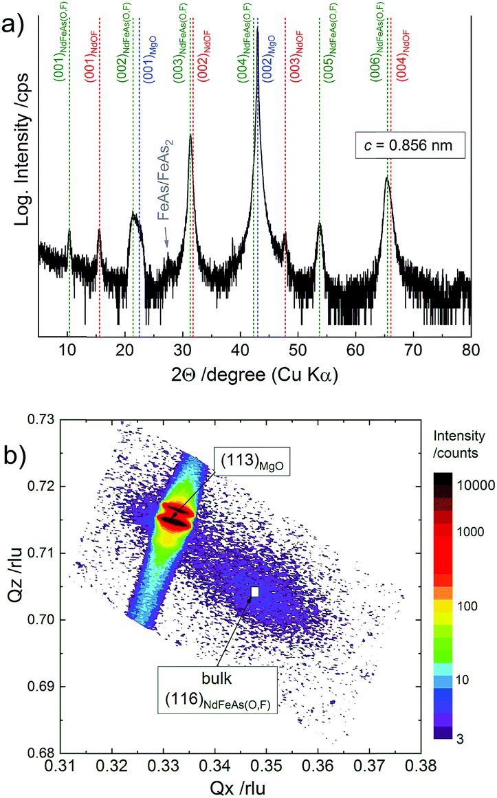 | ||
| Fig. 1 (a) X-ray θ–2θ scan of the MgO/NdFeAs(O,F)/NdOF composite in Bragg–Brentano geometry verifying the c-axis-oriented growth of both NdFeAs(O,F) and NdOF by the presence of (00l)-reflections. (b) Reciprocal space map showing a relatively broad (116) reflection of the NdFeAs(O,F) layer besides the substrate (113)MgO reflection. | ||
A reciprocal space map (RSM, Fig. 1b) was analyzed to get information about the in-plane lattice parameter. The scanned range covers the (113)MgO reflection of the substrate and the (116)NdFeAs(O,F) reflection of the superconducting layer. Two (black) maxima at Qx ≈ 0.33 originate from the Kα1 and Kα2 of (113)MgO. For the (116)NdFeAs(O,F) reflection, a wide range in Qx and Qz values is visible. A broad variation occurs close to the bulk position at Qx ≈ 0.35 and Qz ≈ 0.705 of the NdFeAs(O1−xFx) compound.‡ This peak broadening together with a possible variation in the a-axis lattice parameter might be caused by several reasons: the formation of local strain at dislocation arrays or around small defects (high dislocation density), the influence of the mosaicity in thin films or a variation of the composition of the NdFeAs(O1−xFx) layer. Furthermore, a weak-intensity peak seems to be overlapping with the (113)MgO reflection which could originate from a partially strained layer at the interface to the substrate. However, from this RSM measurement alone one cannot distinguish between the afore-mentioned strain states.
A high-resolution transmission electron microscopy (HRTEM) image (Fig. 2) indicates a dense NdFeAs(O,F) layer with a thickness t of approximately 22 nm. The electron beam, parallel to the [100]NdFeAs(O,F) zone axis, reveals the NdFeAs(O,F) microstructure. Differences in lattice parameters and epitaxial relations between the various layers are determined by fast Fourier transformation (FFT) patterns of several areas in the different layers. The experimentally obtained diffractograms were compared with selected-area diffraction patterns (not shown here) that were calculated by using the JEMS software.21 For the NdFeAs(O,F) layer, the diffractogram shows good agreement with the calculated pattern of tetragonal NdFeAs(O,F) with the space group P4/nmm‡ along its [100] zone axis. As a general result, the epitaxial relation (001)[100]MgO‖(001)[100]NdFeAs(O,F)‖(001)[110]NdOF and good crystalline growth are confirmed. Between the MgO substrate and NdFeAs(O,F) layer, however, an additional thin reaction layer is visible (≤2 nm), which was confirmed by energy-dispersive X-ray spectroscopy (EDXS) as magnesium fluoride (see Fig. 3). No grain boundaries are observable in this field of view. In the HRTEM image of Fig. 2, the atomic columns seem to be much better resolved in the NdFO cap layer than in the adjacent NdFeAs(O,F) layer. However, the blurred image contrast visible in the latter is probably caused by internal strain, correspondingly lattice distortions, as well as larger crystal defects. The NdOF layer is not continuous and consists of trapezoidally shaped regions (as also observed by atomic force microscopy measurement, see ESI†).
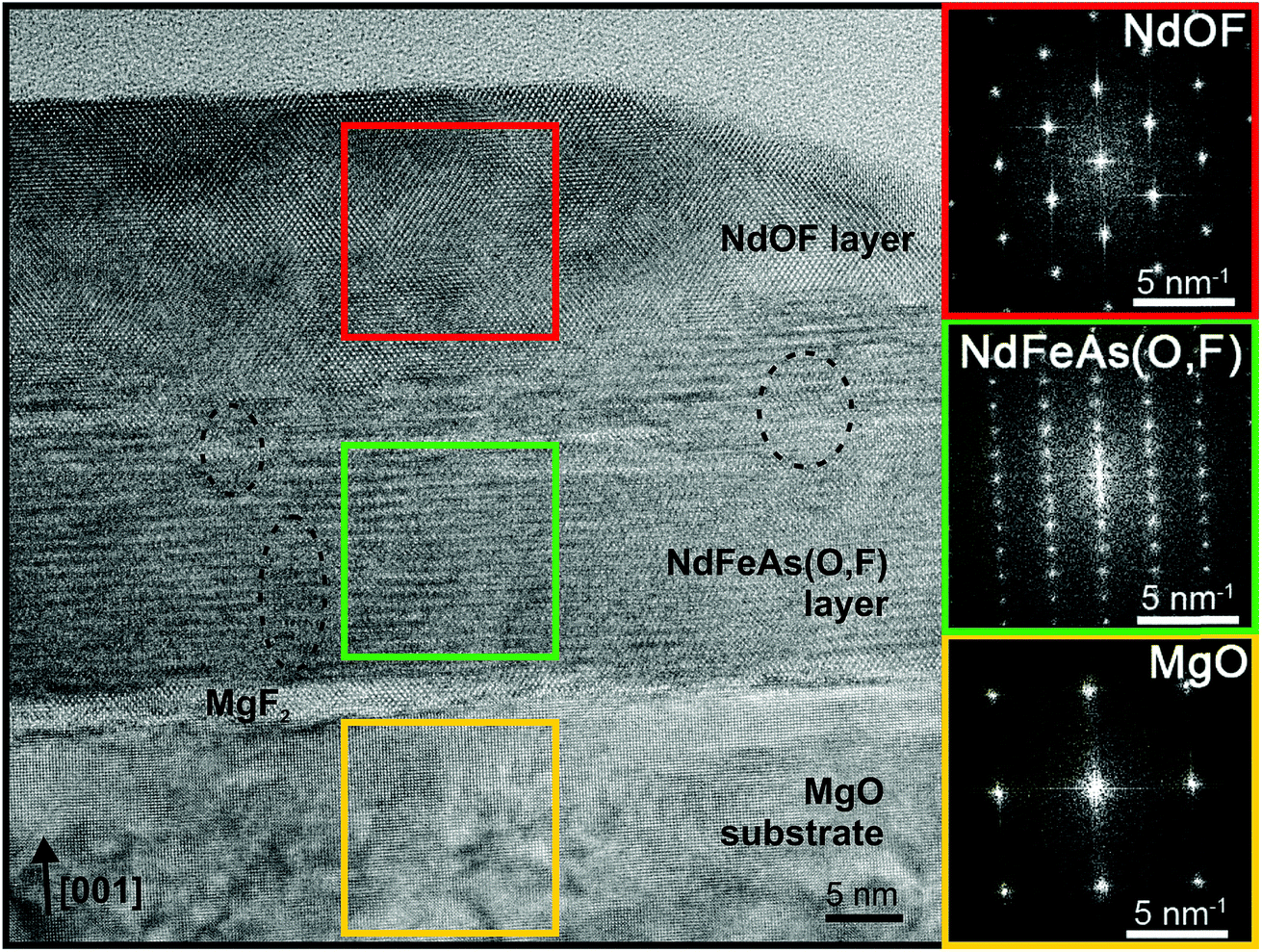 | ||
| Fig. 2 High-resolution TEM micrograph of the MgO/NdFeAs(O,F)/NdOF sample in cross-sectional view and corresponding FFT patterns obtained from the different layer regions marked by colored squares. An epitaxial growth is confirmed, however, the crystal lattice of the NdFeAs(O,F) layer is relatively strongly disturbed. | ||
 | ||
| Fig. 3 Element distribution maps of Fe (a), Nd (b), Mg (c), As (d), O (e) and F (f) of the NdFeAs(O,F)/NdOF layers on MgO measured by energy-dispersive X-ray spectroscopy, showing nonstoichiometries on the nanoscale in the NdFeAs(O,F) layer as described in the text. FeAs/FeAs2 precipitates and a reaction layer composed of magnesium fluoride are also observed. | ||
For a closer look at the local element distribution, atom probe tomography (APT) images were recorded on several samples prepared by a focused ion beam (FIB) technique. From the near-atomic-resolution 3D datasets, element distribution maps of the whole FIB samples (50 nm in width) can be created (Fig. 5), both in the cross-section and within the film plane. As clearly visible, the elements are not homogenously distributed within the NdFeAs(O,F) film. F-rich and Fe-rich local regions as well as metallic, single-element Fe nanoparticles of 2 nm dimension and small NdO precipitates within the superconducting layer are visible. A few FeAs-rich 10 nm wide, elongated precipitates starting at the interface to the substrate are also visible with APT (for further APT images see ESI†). The inhomogeneous distribution of O and F in the cap layer originates from the non-stoichiometry of NdOF. Some segregation seems to take place during the deposition process of the NdOF layer: on the one hand F-rich areas and on the other hand areas rich in FeAs/FeAs2 and NdO are formed.
This pronounced local inhomogeneity of the elements appears to be in contrast to the uniform layer observed in the high-resolution TEM image (Fig. 2). There, only small distorted areas are barely visible (marked by dashed lines). It seems that the F-rich, Fe-rich and Fe–As local regions are not pronounced defects with a clear atomic structure, or, in the case of the 2 nm metallic Fe nanoparticles, are too small to observe with XRD (and perhaps TEM). This is clearly different from microstructures of other FBS films, where self-assembled precipitates of clear crystal structure and morphology are observed, for example 4–5 nm wide nanopillars in epitaxial BaFe2As2 thin films.22
Electrical transport properties
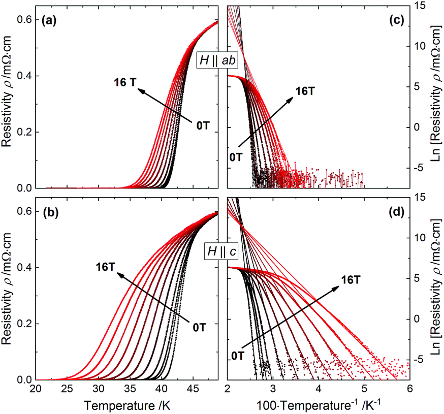 | ||
| Fig. 4 Resistive transitions ρ(T) measured in static magnetic fields up to 16 T for both major directions H‖ab (above) and H‖c (below) in linear representation (a, b) as well as in Arrhenius plots (c, d). | ||
In contrast, the in-field transition temperature of 43.5 K at 16 T as well as ΔT = 6 K for H‖ab indicates that the Tc for H‖ab is less affected by the magnetic field than for H‖c.
The temperature dependencies of the upper critical field, Hc2(T), and the irreversibility field, Hirr(T), as determined from the resistivity curves ρ(T), and the pinning force density Fp (see Experimental – Electrical characterization), show clear differences for H‖c and H‖ab (Fig. 6a). Because of the lack of low-temperature data, only a very limited range of the magnetic phase diagram is accessible, and it is not possible to reliably fit Hc2(T) with a suitable model for FBS. To determine the Hc2 anisotropy near Tc as well as the zero-field orbital upper critical fields and coherence lengths, the slope of Hc2 at Tc for both main directions was calculated by linear fits above 2 T in order to avoid the inhomogeneity-influenced region near Tc. These fits meet at T = 45.0 K which is close to Tc,90. The respective slopes dHc2/dT for H‖c and H‖ab are −2.1 T K−1 and −11.2 T K−1 resulting in an Hc2 anisotropy of γHc2 = 5.1 ± 0.3 at Tc. This value is in good agreement with other 1111 compounds.13,24,25 The (single-band) orbital upper critical fields according to the WHH model1 are 65 ± 1 T and 330 ± 7 T for H‖c and H‖ab respectively, and the corresponding coherence lengths are ξc = 0.44 ± 0.02 nm and ξab = 2.25 ± 0.02 nm. The irreversibility field for both directions could be fitted with the power law Hirr(T) = Hirr(0)(1 − T/Tirr)a. Best fits were achieved with Tirr = 39.2 K, a = 1.38, and Hirr(0) values of 37 T and 125 T for H‖c and H‖ab, respectively.
 | ||
| Fig. 5 Color-coded atomic element distribution of Fe, Nd, Mg, As, O, and F of a NdFeAs(O,F)/NdOF layer on MgO measured by APT, in the vertical cross-section (above), in-plane cut of the cap-layer (middle), and in-plane cut of the superconducting layer (below). Blue means 0 at% and red the corresponding maximum concentration. Small Fe, Fe–As and NdO particles are visible. | ||
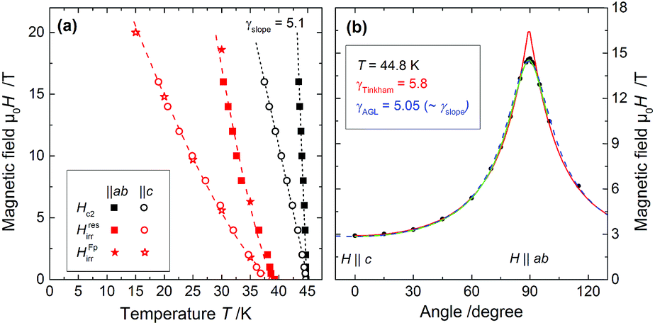 | ||
| Fig. 6 Temperature dependence of the upper critical field, μ0Hc2, and irreversibility field, μ0Hirr, for both major directions. The dashed and dotted curves are power law fits Hirr(T) = Hirr(0)(1 − T/Tirr)a and linear fits to Hc2 above 2 T respectively. (b) Angular dependence of the upper critical field at 44.8 K, i.e. close to Tc,onset. The solid line (red) is a fit using the 2D Tinkham model, the dashed line (blue) represents the one-band anisotropic Ginzburg–Landau (AGL) theory, and the green line the results for the modified AGL model (see text). | ||
The sample's anisotropy near Tc was further evaluated by measuring the angular dependence of the upper critical field, Hc2(θ), where θ is the angle between the applied field and the c-axis. Hc2(θ) was determined from R(B) curves at given angles at 44.8 K. Since the R(T) and the R(B) measurements are separated by half a year, the sample altered slightly (increased normal state resistivity likely due to undesired moisture exposure); Tc,onset, however, was unchanged. Hc2(θ), Fig. 6b, shows as expected a maximum at θ = 90° (H‖ab) and a minimum at θ = 0° (H‖c). The data can be described fairly well using the 3D Anisotropic Ginzburg–Landau (AGL) model26,27 with Hc2(θ) = Hc2c(cos2![[thin space (1/6-em)]](https://www.rsc.org/images/entities/char_2009.gif) θ + γ−2sin2θ)−0.5, blue line in Fig. 6b. However, even though the fit describes the data nicely near H‖c and H‖ab, it clearly deviates from the data at medium angles.
θ + γ−2sin2θ)−0.5, blue line in Fig. 6b. However, even though the fit describes the data nicely near H‖c and H‖ab, it clearly deviates from the data at medium angles.
There are two possible reasons for this behavior: firstly, different extended defects as observed in TEM (Fig. 3) and APT (Fig. 5) may lead to extra contributions near the two major directions and consequently alter the anisotropy of the coherence lengths. This effect has been described for columnar defects in irradiated Sm1111 single crystals28 as well as ab-planar defects in CaAlSi single crystals29 and has been discussed for Co-doped30 and P-doped31 BaFe2As2 (Ba122) thin films with several different growth defects. In fact, following the modified AGL model in those references, which has recently been generalized by Talantsev and Mataira,32 and decreasing the exponent in the above equation to 1.85 lead to a near-perfect fit (green curve in Fig. 6b). Secondly, recently a mixture of 2D and 3D fluctuations has been described by Galeski et al. on Sm1111 nanocrystals which may extend the temperature region of low-temperature 2D behavior (below the expected dimensional cross-over temperature Tco = Tc(1 − (ξc/d)2) = 35 K with d = 0.8 nm) close to Tc since 2D fluctuations may screen the 3D ones.33 Indeed, a fit according to the Tinkham model34 for 2D superconductors |Hc2(θ)sinθ/Hc2c| + |Hc2(θ)cosθ/Hc2ab|2 = 1 (we used it in the form of eqn (3) of ref. 35) to the low- and medium-angle data with Hc2‖c as the fixed parameter (red line in Fig. 6b) results in a very good agreement with the data up to 85° for γTink = 5.8. This value, however, is slightly higher than γHc2 = 5.1 ± 0.3. A very similar mix of 2D and 3D Hc2 anisotropy behavior near Tc had been found for Bi2Sr2CaCu2Ox single crystals by Marcon et al.36 To determine whether one of these two effects and which one might be responsible for the observed Hc2 anisotropy would need further investigations.
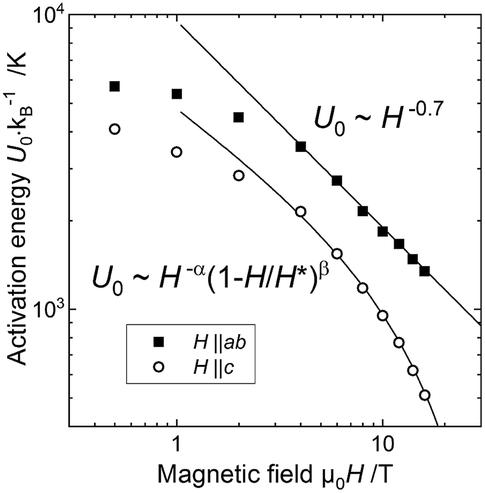 | ||
| Fig. 7 Field dependence of the pinning potential for both major directions. The solid lines are fits to the equations, see text. | ||
Due to the lack of high-field data above 16 T, the exponents as well as H*, which is close to Hirr(0 K), cannot be determined with absolute certainty. Nevertheless, setting α = p − 1 with p ∼ 0.7 as determined in Fp scaling (see below), good agreement with the data was achieved with, e.g., α = 0.3, β = 5 and H* = 70 T. These values are reasonable, whereas α = 0.5 and β = 2 as often used and leading to similarly good fits yield an unrealistically low H* of 45 T. For H‖ab the lack of high-field data is even more problematic and the second factor in the above equation cannot be determined at all. Nevertheless, above 3 T U0 follows a power law with α = 0.7 for that direction. At lower fields, the data differ from these functions because of the crossover to the regime of single vortex pinning, where U0 is constant. The value of this cross-over field to single vortex pinning of ∼2–3 T is comparable to literature data on Nd1111, La1111, and Sm1111 (ref. 38 and references therein).
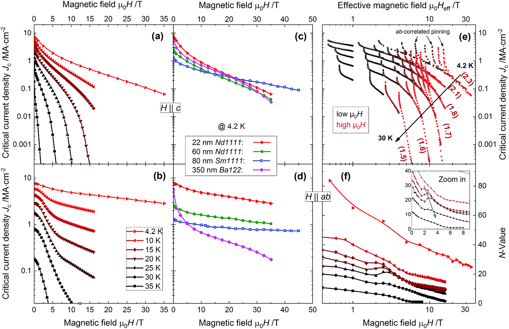 | ||
| Fig. 8 Field dependence of the critical current density for both major directions H‖c (above) and H‖ab (below) at various temperatures between 4.2 K and 35 K (a, b), and in comparison to data for other 1111 and Co-doped Ba122 from ref. 11, 12, and 39 at 4.2 K (c, d). Anisotropic Ginzburg–Landau scaling (e) of the angular dependence Jc(θ) with the used anisotropy parameter γJ written in brackets. The curves were measured up to 16 T between 35 K and 10 K and up to 35 T at 4.2 K. Deviations from scaling occur due to ab-correlated pinning. (f) N-value at various temperatures between 4.2 K and 35 K. Inset: zoom in close to the matching field (arrow) observed between 2.4 T and 3 T (depending on temperature). | ||
Compared to earlier investigations on other 1111 compounds11,12 (Fig. 8c and d), Jc,sf is more than doubled. Only for H‖c and fields above 25 T does the Sm1111 take over. Other FBS like Co-doped Ba122 exhibit a lower self-field Jc,sf. For example a 350 nm thick Ba(Fe1−xCox)2As2 film39 exhibits Jc,sf ∼ 5.6 MA cm−2 at 4.2 K and Jc for H‖ab of 0.18 MA cm−2 at 35 T (Fig. 8d). A BaFe2(As,P)2 film23 shows a Jc,sf of up to 6.5 MA cm−2 at 4.2 K and a Jc for H‖ab of 0.1 MA cm−2 at 30 T (not shown here). This shows that the decrease in Jc with increasing field is much more pronounced in Ba122 compared to 1111 compounds. Another study on P-doped Ba122 (ref. 40) showed a Jc,sf of 12 MA cm−2 by magnetization and 7 MA cm−2 by transport, but the field dependence was not measured. The reason for the high Jc is not clear; the authors supposed the formation of Fe nanoparticles or layers, which however could not be observed with the applied X-ray diffraction. The reasons for the lower Jc values in the 60 nm Nd1111 film12 can be manifold: a different microstructure (e.g. F-content, precipitates), less strain effect (as deduced from a different F-content series, not shown here) and larger thickness itself.41
The angular dependencies of the critical current density Jc(θ) (Fig. 9) show for all fields and temperatures one maximum at H‖ab (θ = 90°), which becomes sharper with increasing field or temperature. No second local maximum at H‖c due to correlated defects arises. The absence of this peak is in agreement with the TEM observations, where no nanocolumns are visible (Fig. 2). Point defects as well as the randomly distributed small precipitates of different compositions seem to act as more or less isotropic pinning and lead to a general increase in Jc over the complete angular range.
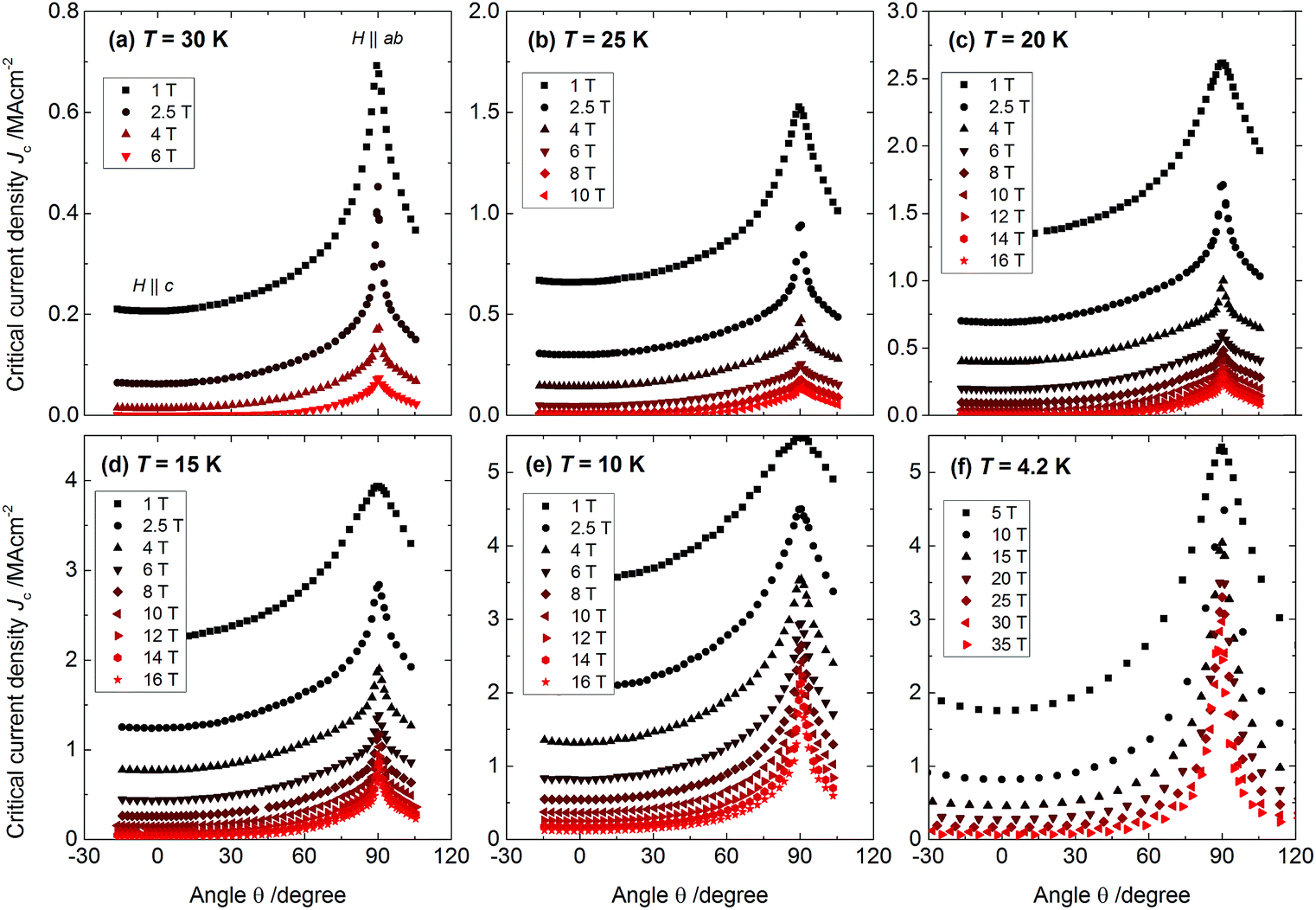 | ||
| Fig. 9 Angular dependence of the critical current density Jc at (a) 30 K, (b) 25 K, (c) 20 K, (d) 15 K, (e) 10 K and (f) 4.2 K for various magnetic fields. | ||
To identify pinning contributions originating from these random uncorrelated (isotropic) defects, the Jc(θ) curves were analyzed using the AGL scaling approach introduced by Blatter et al.42,43 This scaling approach was developed for single-band superconductors but has also been successfully applied to multiband materials of FBS like Co-doped Ba112 (ref. 44) and La1111.13 The Jc data are scalable in an effective magnetic field  . To rescale the data onto a single trend line (Fig. 8e), the Jc anisotropy parameter γJ has to be increased with decreasing temperature. It ranges from 1.5 at 30 K to 2.3 at 4.2 K. A temperature-dependent anisotropy is typical for multi-band superconductors45 and was verified for FBS12,13,44,46,47 as different bands contribute to Jc at different temperatures. However, different trends of the temperature dependence of γJ have been reported in the literature depending on the compound and dimensionality.12,13,47 Up to now, the reason for those differences in temperature dependence is not completely understood, nevertheless decreasing γJ values for decreasing temperatures are often found for 3D FBS materials such as Ba122 compounds and increasing values for 2D compounds. Furthermore, the anisotropy γJ of the 22 nm sample (1.5–2.3) is lower than γHc2 = 5.1. This is, generally, due to the influence of extended and correlated defects.
For FBS, the ξ and λ anisotropies are different (i.e. ξab/ξc ≠ λc/λab) due to the multi-band state and the crossover between 2D and 3D vortex behavior (see, e.g.ref. 12). In our films, the increase of the Jc anisotropy γJ with decreasing temperature is similar to the penetration depth anisotropy γλ;12 only the magnitude of γJ is smaller than that of γλ.46 This indicates that both intrinsic and extrinsic parameters and also the crossover between 2D and 3D behavior affect Jc.12
The scaling of Jc on Heff also exposes possible ab-planar and c-axis-correlated pinning through deviations from the envelope function. In our films, such deviations occur only at H‖ab, due to ab-correlated pinning, which is more pronounced at higher fields (examples are marked by black arrows in Fig. 8e) at low as well as higher temperatures. A strong and pronounced deviation for H‖ab at higher temperatures could be an indication for vortex interactions with the surface since the thickness-to-penetration depth ratio (t/λ) decreases at higher temperatures. On the other hand, no hint for c-axis-correlated pinning (i.e. deviation from scaling) is visible.
The I–V curves, from which Jc was determined, are described by the power-law relation V ∼ IN around Jc in the entire field and temperature range. The N value (Fig. 8f) is in general influenced by sample homogeneity and flux creep rate S,48–51 where the former prevails in low-Tc superconductors and the latter in cuprates and FBS with relatively large fluctuation regimes, i.e. Ginzburg numbers Gi. Neglecting inhomogeneities, the creep rate S can be approximated as S = 1/(N − 1). N (as well as Jc) is usually proportional (or positively correlated) to the pinning potential U. Therefore, in general a power-law relation of the type N ∼ Jcz has been found e.g. for YBa2Cu3O7 (ref. 52) and Nd1111 (ref. 12) in the case of random isotropic pinning, independent of temperature, field and angle. This correlation has nevertheless also been reported for inhomogeneity-driven superconductors, e.g. for MgB2, NbTi, and Nb3Sn.53–55 Accordingly, an increase of Jc leads to an increase in the N value, and as a consequence Jc(H) and N(H) should have similar trends. For H‖ab, the 22 nm NdFeAs(O,F) film (Fig. 8b and f) shows this trend at low (4.2 K) and high temperatures (35 K). Between 15 and 25 K, however, a small maximum in N(H) is formed at around 2.4 T. Such regions of inverse correlation between Jc and N are usually hints for further contributions to the creep rate such as formation of vortex kinks and double kink structures at highly correlated pinning centers leading to increased creep rates if not suppressed by matching densities of vortices and defects, which is called the matching-field effect as discussed later in the paper.
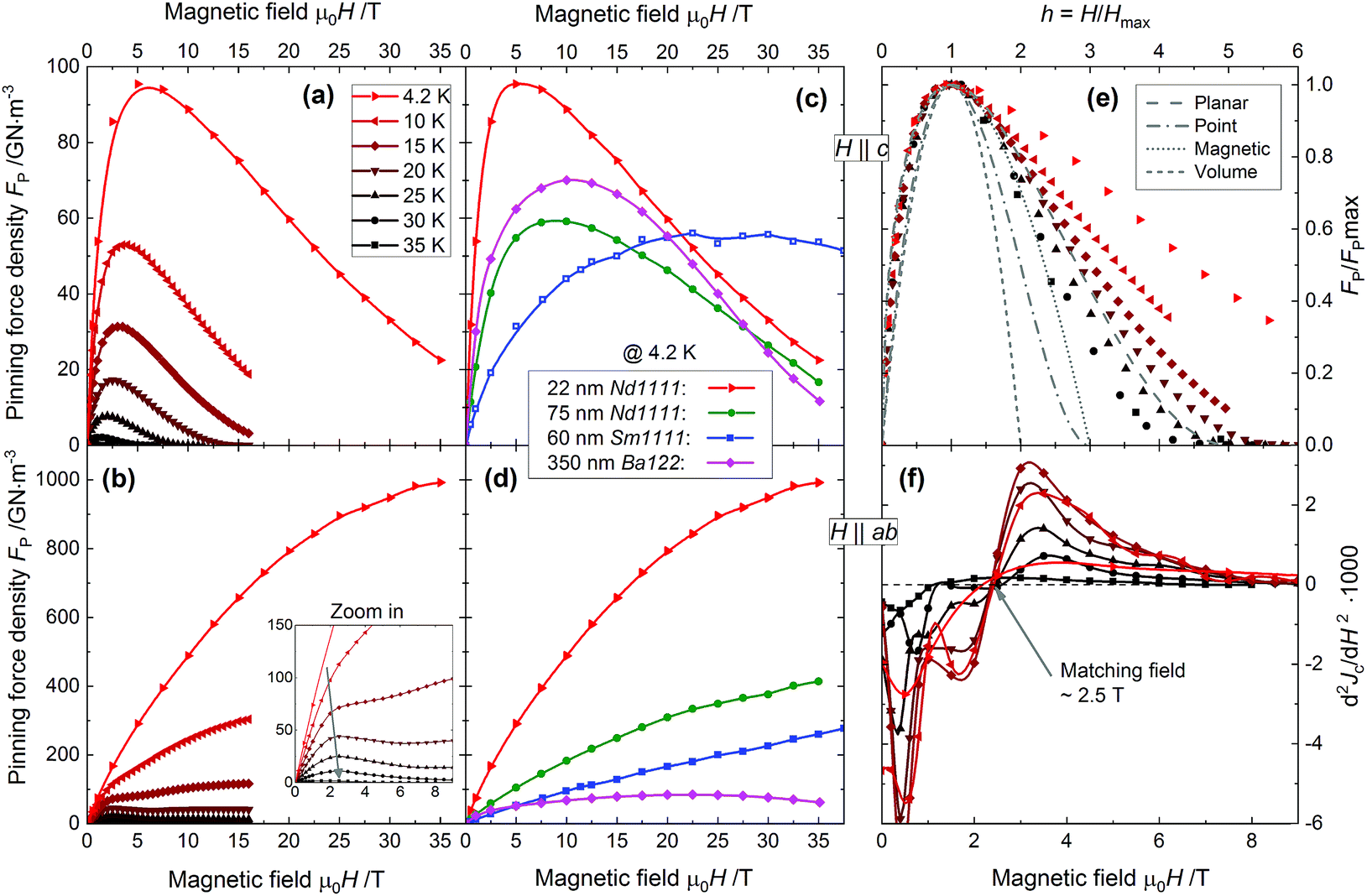 | ||
| Fig. 10 Field dependence of flux pinning density Fp for both major directions H‖c (above) and H‖ab (below) for various temperatures between 4.2 K and 35 K (a and b), and in comparison to data for other Ln1111 compounds from ref. 11, 33, and 34 at 4.2 K (c and d). The normalized pinning force density as a function of reduced field h (e). The different lines represent different pinning mechanisms (point, planar, magnetic and volume pinning), where the pinning is dominated by planar defects. (f) Second derivative of Jc(H) showing the matching field (∼2.4 T) (see also inset (b)) for different temperatures by crossing the zero-line. | ||
Usually, the normalized pinning force density fp = Fp/Fp,max is plotted as a function of reduced field h = H/Hirr for superconductors with large vortex liquid regions such as cuprates and FBS. Instead, we plot fp for H‖c as a function of h* = H/Hmax (where Hmax = H(Fp,max)) since Jc could not be measured up to Hirr at all temperatures (Fig. 10e). Similar scaling has been used earlier also for YBa2Cu3O7 (ref. 56) and FBS.31 For H‖c, Fp(H) is analyzed using the modified Dew-Hughes model, where the original scaling field Hc2 is replaced by Hirr. fp ∝ hp(1 − h)q ∝ h*p({p + q}/p − h*)q where p and q are free parameters, dependent on the pinning mechanism.57 For H‖ab, we could not follow this approach because the maximum Fp is not reached.
Attempts to fit fp(h) or fp(h*) with a single such Dew-Hughes function were not successful, especially at low T, which suggests that more than one pinning mechanism is present. Nevertheless, the normalized fp(H‖c) curves scale roughly onto one master curve below h* < 1 (Fig. 10e), indicating that the same pinning mechanism contributes to Jc at all temperatures in this field range. The exponent p is around 0.7 for all temperatures for H‖c. According to ref. 56, that suggests strong pinning centers slightly larger than ξab, which is in accord with the nanoparticle precipitation seen in TEM and APT. In the high-field range, fp varies systematically with temperature and field strength. Therefore, specific functions with different p and q parameters57 are presented in Fig. 10e: (1) a parameter set of (p,q) = (0.5,1) describes magnetic pinning, (2) (p,q) = (1,1) volume pinning, (3) (p,q) = (0.5,2) planar pinning on two-dimensional non-magnetic defects and (4) (p,q) = (1,2) point pinning on non-superconducting particles.57 Below h < 1 the data at all temperatures are closer to both magnetic and planar pinning with (p,q) = (0.5,1) and (0.5,2). Since switching of magnetic domains happens below 200 mT and magnetic pinning is dominated by the penetration depth λ, magnetic pinning (if at all) only contributes at very low fields. For higher fields, planar pinning on two-dimensional defects dominates such as small-angle grain boundaries or dislocation networks although they have not been directly confirmed in the TEM investigations. Also the model proposed by Kramer for flux shearing on arrays of 1D defects generates a similar functional dependence to planar pinning.58 Another type of magnetic pinning, different from the mechanism described by Dew-Hughes might be possible in these films. In case the elemental Fe nanoparticles are not superparamagnetic, they might contribute magnetically to the pinning force via a reduction of Lorentz force by the additional magnetic flux as described by Blamire et al.59 In that case, it would not be limited to the smallest fields.
In the field dependence of Fp (Fig. 10b, inset) and of the N value for H‖ab (Fig. 8f), peaks at around 2.5 T are found. This peak effect is further evidenced by zero transition of the second derivative of Jc(H) (Fig. 10f). The matching field B0 for H‖ab is calculated as 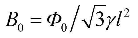 , where l is the vortex row separation in the c-direction and γ the relevant anisotropy. If l would be equal to the c-axis lattice parameter of 0.856 nm, the matching field would amount to ∼200 T, and hence, one can exclude this kind of intrinsic pinning. Assuming instead n equally spaced vortex rows across the film thickness leads to
  , where t = 22 nm is the film thickness as determined by TEM. The lowest possible matching field configuration is a single row in the center of the film due to the strong Bean–Livingston barriers60 on both interfaces (i.e. substrate/NdFeAs(O,F) and NdOF/NdFeAs(O,F)). In that case, and assuming the relevant anisotropy parameter is γJ(T) (Fig. 8), the temperature-dependent matching field position is shown in the inset of Fig. 8f and corresponds nicely to the peak positions in N(H). This can be explained in terms of the most stable vortex configuration where excited structures such as kinks and double kinks as well as displacements are most effectively suppressed leading to reduced creep rates S and consequently to a maximum in N. On the contrary, for around half filling of such a single row (at B0/2), a minimum in N(H) can be observed since such excited structures and therefore creep are most probable around these fields. Higher orders of vortex row configurations may be guessed for n = 2 or 3 but cannot be observed unambiguously due to increased noise levels at low Jc and N. For thicker films this matching effect has not been observed. For the 60 nm film in ref. 12, e.g., the peak is expected at B0 = 0.39…0.44 T for temperatures of 4.2…30 K. In this field range, N(B) is much steeper and the scatter in N is larger due to the lower number of data points in V(I) and N(B). A possibly larger surface roughness of the 60 nm film as well as a larger freedom of the vortices to rearrange across the film thickness would further wash out such matching effects.
These matching effects, in combination with the strong pinning by the nanoscale inhomogeneities (Fe-rich, Fe–As, NdFeO precipitates) and potentially the magnetic contribution to pinning by the Fe particles lead to the observed superior pinning force densities and in-field critical current densities in this 22 nm NdFeAs(O,F) film, especially for H‖ab.
Conclusions
The structural and electrical properties of a superconducting epitaxial 22 nm NdFeAs(O1−xFx) thin film on a MgO single crystalline substrate were analyzed. Near-atomic-resolution measurements with TEM and APT reveal nanoscale inhomogeneities in the element distribution. The thin film contains small Fe nanoparticles and other Fe- and O-rich phases of different size, shape and orientation distribution. The electrical transport properties were measured in high magnetic fields. The interplay between small nanoparticles, ab-planar pinning centers, and intrinsic pinning as well as matching effects related to the film thickness leads to high Jc (Jc,sf ≈ 7.6 MA cm−2 at 4.2 K) and Fp ∼ 1 TN m−3 for H‖ab (4.2 K, 35 T) respectively. The angular dependence of Hc2(θ) is influenced by the multi-band superconductivity which also influences Jc(θ) where Jc can be scaled in a wide angular range by the Anisotropic Ginzburg–Landau approach.Conflicts of interest
There are no conflicts to declare.Author contributions
SKW, KI and JH designed the study. SKW, TO, TM and TH prepared the films by molecular beam epitaxy (MBE) at Nagoya University. SM, CT, JJ and KI measured the high-field properties up to 35 T at NHMFL Tallahassee. CT, SKW, SM and JH measured and analysed further in-field transport data up to 14 (at KIT) and 16 T (at NHMFL). TB took care of the atom probe tomography (APT) investigations, RS and DG the transmission electron microscopy (TEM) studies. SKW and ML investigated the microstructure by X-ray diffraction (XRD). HI and BH supervised parts of the project. The manuscript was written by SKM together with KI, JH and CT, where all co-authors contributed to style and content at different stages of writing.Acknowledgements
The authors thank Dominic Barthlott (KIT, ITEP) for experimental support and Delphine Chassaing (KIT, IAM-WK) for the FIB preparation of APT samples. This work was supported by the JSPS Grant-in-Aid for Scientific Research (B) Grant Number 16H04646 as well as JST CREST Grant Number JPMJCR18J4. A portion of this work was performed at the National High Magnetic Field Laboratory, which is supported by National Science Foundation Cooperative Agreement No. DMR-1644779, DMR-1157490 and the State of Florida.Notes and references
- N. R. Werthamer, E. Helfand and P. C. Hohenberg, Temperature and Purity Dependence of the Superconducting Critical Field, Hc2 III. Electron Spin and Spin-Orbit Effects, Phys. Rev., 1966, 147, 295–302, DOI:10.1103/PhysRev.147.295.
- J.-l. Zhang, L. Jiao, Y. Chen and H.-q. Yuan, Universal behavior of the upper critical field in iron-based superconductors, Front. Phys., 2011, 6, 463–473, DOI:10.1007/s11467-011-0235-7.
- J. Hänisch, K. Iida, R. Hühne and C. Tarantini, Fe-based superconducting thin films – preparation and tuning of superconducting properties, Supercond. Sci. Technol. DOI:10.1088/1361-6668/ab1c00.
- M. Fujioka, S. J. Denholme, T. Ozaki, H. Okazaki, K. Deguchi, S. Demura, H. Hara, T. Watanabe, H. Takeya, T. Yamaguchi, H. Kumakura and Y. Takano, Phase diagram and superconductivity at 58.1 K in α-FeAs-free SmFeAsO1−xFx, Supercond. Sci. Technol., 2013, 26, 085023, DOI:10.1088/0953-2048/26/8/085023.
- S. Takeda, S. Ueda, S. Takano, A. Yamamoto and M. Naito, Growth of superconducting SmFeAs(O, F) epitaxial films by F diffusion, Supercond. Sci. Technol., 2012, 25, 035007, DOI:10.1088/0953-2048/25/3/035007.
- A. L. Ivanovskii, New high-temperature superconductors based on rare-earth and transition metal oxyarsenides and related phases: synthesis, properties and simulations, Phys.-Usp., 2008, 51, 1229–1260, DOI:10.1070/PU2008v051n12ABEH006703.
- R. Kappenberger, S. Aswartham, F. Scaravaggi, C. G. F. Blum, M. I. Sturza, A. U. B. Wolter, S. Wurmehl and B. Büchner, Solid state single crystal growth of three-dimensional faceted LaFeAsO crystals, J. Cryst. Growth, 2018, 483, 9–15, DOI:10.1016/j.jcrysgro.2017.11.006.
- J. Karpinski, N. D. Zhigadlo, S. Katrych, Z. Bukowski, P. J. W. Moll, S. Weyeneth, H. Keller, R. Puzniak, M. Tortello, D. Daghero, R. Gonnelli, I. Maggio-Aprile, Y. Fasano, Ø. Fischer, K. Rogacki and B. Batlogg, Single crystals of LnFeAsO1−xFx (Ln=La, Pr, Nd, Sm, Gd) and Ba1−xRbxFe2As2: Growth, structure and superconducting properties, Phys. C, 2009, 469, 370–380, DOI:10.1016/j.physc.2009.03.048.
- H. Hiramatsu, T. Katase, T. Kamiya and H. Hosono, Thin Film Growth and Device Fabrication of Iron-Based Superconductors, J. Phys. Soc. Jpn., 2012, 81, 011011, DOI:10.1143/JPSJ.81.011011.
- M. Chihara, N. Sumiya, K. Arai, A. Ichinose, I. Tsukada, T. Hatano, K. Iida and H. Ikuta, Direct growth of superconducting NdFeAs(O,F) thin films by MBE, Phys. C, 2015, 518, 69–72, DOI:10.1016/j.physc.2015.03.022.
- K. Iida, J. Hänisch, C. Tarantini, F. Kurth, J. Jaroszynski, S. Ueda, M. Naito, A. Ichinose, I. Tsukada, E. Reich, V. Grinenko, L. Schultz and B. Holzapfel, Oxypnictide SmFeAs(O,F) superconductor: a candidate for high-field magnet applications, Sci. Rep., 2013, 3, 2139, DOI:10.1038/srep02139.
- C. Tarantini, K. Iida, J. Hänisch, F. Kurth, J. Jaroszynski, N. Sumiya, M. Chihara, T. Hatano, H. Ikuta, S. Schmidt, P. Seidel, B. Holzapfel and D. C. Larbalestier, Intrinsic and extrinsic pinning in NdFeAs(O,F): vortex trapping and lock-in by the layered structure, Sci. Rep., 2016, 6, 36047, DOI:10.1038/srep36047.
- M. Kidszun, S. Haindl, T. Thersleff, J. Hänisch, A. Kauffmann, K. Iida, J. Freudenberger, L. Schultz and B. Holzapfel, Critical Current Scaling and Anisotropy in Oxypnictide Superconductors, Phys. Rev. Lett., 2011, 106, 137001, DOI:10.1103/PhysRevLett.106.137001.
- P. J. W. Moll, R. Puzniak, F. F. Balakirev, K. Rogacki, J. Karpinski, N. D. Zhigadlo and B. Batlogg, High magnetic-field scales and critical currents in SmFeAs(O, F) crystals, Nat. Mater., 2010, 9, 628–633, DOI:10.1038/nmat2795.
- H. Uemura, T. Kawaguchi, T. Ohno, M. Tabuchi, T. Ujihara, Y. Takeda and H. Ikuta, Substrate dependence of the superconducting properties of NdFeAs(O,F) thin films, Solid State Commun., 2012, 152, 735–739, DOI:10.1016/j.ssc.2012.01.037.
- T. Kawaguchi, H. Uemura, T. Ohno, M. Tabuchi, T. Ujihara, Y. Takeda and H. Ikuta, Molecular Beam Epitaxy Growth of Superconducting NdFeAs(O,F) Thin Films Using a F-Getter and a Novel F-Doping Method, Appl. Phys. Express, 2011, 4, 083102, DOI:10.1143/APEX.4.083102.
- D. J. Larson, T. J. Prosa, R. M. Ulfig, B. P. Geiser and T. F. Kelly, Local Electrode Atom Probe Tomography. A User's Guide, Springer New York, New York, NY, s.l., 2013 Search PubMed.
- G. Rupp, E. Springer and S. Roth, Critical current of multifilamentary Nb3Sn conductors up to 18 t, Cryogenics, 1977, 17, 141–144, DOI:10.1016/0011-2275(77)90273-9.
- M. Suenaga and D. O. Welch, in Filamentary A15 Superconductors, ed. M. Suenaga and A. F. Clark, Springer, Boston, MA, 1980, pp. 131–142 Search PubMed.
- J. B. Nelson and D. P. Riley, An experimental investigation of extrapolation methods in the derivation of accurate unit-cell dimensions of crystals, Proc. Phys. Soc., 1945, 57, 160–177, DOI:10.1088/0959-5309/57/3/302.
- P. A. Stadelmann, EMS - a software package for electron diffraction analysis and HREM image simulation in materials science, Ultramicroscopy, 1987, 21, 131–145, DOI:10.1016/0304-3991(87)90080-5.
- Y. Zhang, C. T. Nelson, S. Lee, J. Jiang, C. W. Bark, J. D. Weiss, C. Tarantini, C. M. Folkman, S.-H. Baek, E. E. Hellstrom, D. C. Larbalestier, C.-B. Eom and X. Pan, Self-assembled oxide nanopillars in epitaxial BaFe2As2 thin films for vortex pinning, Appl. Phys. Lett., 2011, 98, 42509, DOI:10.1063/1.3532107.
- F. Kurth, C. Tarantini, V. Grinenko, J. Hänisch, J. Jaroszynski, E. Reich, Y. Mori, A. Sakagami, T. Kawaguchi, J. Engelmann, L. Schultz, B. Holzapfel, H. Ikuta, R. Hühne and K. Iida, Unusually high critical current of clean P-doped BaFe2As2 single crystalline thin film, Appl. Phys. Lett., 2015, 106, 072602, DOI:10.1063/1.4908257.
- S. Haindl, K. Hanzawa, H. Sato, H. Hiramatsu and H. Hosono, In-situ growth of superconducting SmO1−xFx FeAs thin films by pulsed laser deposition, Sci. Rep., 2016, 6, 3296, DOI:10.1038/srep35797.
- Z. Pribulova, T. Klein, J. Kacmarcik, C. Marcenat, M. Konczykowski, S. L. Bud’ko, M. E. Tillman and P. C. Canfield, Upper and lower critical magnetic fields of superconducting NdFeAsO1−xFx single crystals studied by Hall-probe magnetization and specific heat, Phys. Rev. B, 2009, 79, 020508(R), DOI:10.1103/PhysRevB.79.020508.
- W. E. Lawrence and S. Doniach, Theory of Layer Structure Superconductors, Proceedings of the Twelfth International Conference on Low Temperature Physics, 1971, pp. 361–362 Search PubMed.
- G. Blatter, M. V. Feigel'man, V. B. Geshkenbein, D. J. Larkin and V. M. Vinokur, Vortices in high-temperature superconductors, Rev. Mod. Phys., 1994, 66, 1126–1388 CrossRef.
- L. Fang, Y. Jia, V. Mishra, C. Chaparro, V. K. Vlasko-Vlasov, A. E. Koshelev, U. Welp, G. W. Crabtree, S. Zhu, N. D. Zhigadlo, S. Katrych, J. Karpinski and W. K. Kwok, Huge critical current density and tailored superconducting anisotropy in SmFeAsO0.8F0.15 by low-density columnar-defect incorporation, Nat. Commun., 2013, 4, 3296, DOI:10.1038/ncomms3655.
- A. K. Ghosh, M. Tokunaga and T. Tamegai, Angular dependence of the upper critical field in CaAlSi single crystal: Deviation from the Ginzburg-Landau anisotropic mass model, Phys. Rev. B: Condens. Matter Mater. Phys., 2003, 68, 63, DOI:10.1103/PhysRevB.68.054507.
- J. Hänisch, K. Iida, F. Kurth, E. Reich, C. Tarantini, J. Jaroszynski, T. Förster, G. Fuchs, R. Hühne, V. Grinenko, L. Schultz and B. Holzapfel, High field superconducting properties of Ba(Fe1−xCox)2As2 thin films, Sci. Rep., 2015, 5, 17363, DOI:10.1038/srep17363.
- K. Iida, H. Sato, C. Tarantini, J. Hänisch, J. Jaroszynski, H. Hiramatsu, B. Holzapfel and H. Hosono, High-field transport properties of a P-doped BaFe2As2 film on technical substrate, Sci. Rep., 2017, 7, 39951, DOI:10.1038/srep39951.
- E. F. Talantsev and R. C. Mataira, Polar projections for big data analysis in applied superconductivity, AIP Adv., 2018, 8, 75213, DOI:10.1063/1.5038040.
- S. Galeski, P. J. W. Moll, N. D. Zhigadlo, K. Mattenberger and B. Batlogg, Critical fields and fluctuations determined from specific heat and magnetoresistance in the same nanogram SmFeAs(O,F) single crystal, Phys. Rev. B, 2017, 96, 104511, DOI:10.1103/PhysRevB.96.104511.
- M. Tinkham, Effect of Fluxoid Quantization on Transitions of Superconducting Films, Phys. Rev., 1963, 129, 2413–2422, DOI:10.1103/PhysRev.129.2413.
- R. Fastampa, M. Giura, R. Marcon and E. Silva, 2D to 3D crossover in Bi-Sr-Ca-Cu-O: comparison with synthetic multilayered superconductors, Phys. Rev. Lett., 1991, 67, 1795–1798, DOI:10.1103/PhysRevLett.67.1795.
- R. Marcon, R. Fastampa, M. Giura and E. Silva, Anisotropy and Dimensionality in the Resistive Measurements in Epitaxial Films of BiSrCaCuO, Europhys. Lett., 1991, 16, 757–762, DOI:10.1209/0295-5075/16/8/009.
- J. R. Thompson, K. D. Sorge, C. Cantoni, H. R. Kerchner, D. K. Christen and M. Paranthaman, Vortex pinning and slow creep in high- Jc MgB2 thin films: a magnetic and transport study, Supercond. Sci. Technol., 2005, 18, 970–976, DOI:10.1088/0953-2048/18/7/008.
- J. Hänisch, K. Iida, T. Ohmura, T. Matsumoto, T. Hatano, M. Langer, S. Kauffmann-Weiss, H. Ikuta and B. Holzapfel, Vortex glass-liquid transition and activated flux motion in an epitaxial, superconducting NdFeAs(O,F) thin film, Magn. Reson. Chem., 2018, 47, 1–6, DOI:10.1557/mrc.2018.207.
- C. Tarantini, F. Kametani, S. Lee, J. Jiang, J. D. Weiss, J. Jaroszynski, E. E. Hellstrom, C.-B. Eom and D. C. Larbalestier, Development of very high Jc in Ba(Fe1-xCox)2As2 thin films grown on CaF2, Sci. Rep., 2014, 4, 7305, DOI:10.1038/srep07305.
- A. Sakagami, T. Kawaguchi, M. Tabuchi, T. Ujihara, Y. Takeda and H. Ikuta, Critical current density and grain boundary property of BaFe2(As,P)2 thin films, Phys. C, 2013, 494, 181–184, DOI:10.1016/j.physc.2013.04.047.
- A. Gurevich, Pinning size effects in critical currents of superconducting films, Supercond. Sci. Technol., 2007, 20, S128–S135, DOI:10.1088/0953-2048/20/9/S03.
- G. Blatter, V. B. Geshkenbein and D. J. Larkin, From isotropic to anisotropic superconductors: a scaling approach, Phys. Rev. Lett., 1992, 68, 875–878, DOI:10.1103/PhysRevLett.68.875.
- L. Civale, B. Maiorov, A. Serquis, J. O. Willis, J. Y. Coulter, H. Wang, Q. X. Jia, P. N. Arendt, M. Jaime, J. L. MacManus-Driscoll, M. P. Maley and S. R. Foltyn, Understanding high critical currents in YBa2Cu3O7 thin films and coated conductors, J. Low Temp. Phys., 2004, 135, 87–98 CrossRef CAS.
- K. Iida, J. Hänisch, T. Thersleff, F. Kurth, M. Kidszun, S. Haindl, R. Hühne, L. Schultz and B. Holzapfel, Scaling behavior of the critical current in clean epitaxial Ba(Fe1−xCox)2As2 thin films, Phys. Rev. B: Condens. Matter Mater. Phys., 2010, 81, 100507R, DOI:10.1103/PhysRevB.81.100507.
- J. D. Fletcher, A. Carrington, O. J. Taylor, S. M. Kazakov and J. Karpinski, Temperature-dependent anisotropy of the penetration depth and coherence length of MgB2, Phys. Rev. Lett., 2005, 95, 097005, DOI:10.1103/PhysRevLett.95.097005.
- S. Weyeneth, R. Puzniak, N. D. Zhigadlo, S. Katrych, Z. Bukowski, J. Karpinski and H. Keller, Evidence for Two Distinct Anisotropies in the Oxypnictide Superconductors SmFeAsO0.8F0.2 and NdFeAsO0.8F0.2, J. Supercond. Novel Magn., 2009, 22, 347–351, DOI:10.1007/s10948-009-0445-1.
- K. Iida, J. Hänisch, E. Reich, F. Kurth, R. Hühne, L. Schultz, B. Holzapfel, A. Ichinose, M. Hanawa, I. Tsukada, M. Schulze, S. Aswartham, S. Wurmehl and B. Büchner, Intrinsic pinning and the critical current scaling of clean epitaxial Fe(Se,Te) thin films, Phys. Rev. B: Condens. Matter Mater. Phys., 2013, 87, 104510, DOI:10.1103/PhysRevB.87.104510.
- W. H. Warnes and D. C. Larbalestier, Analytical technique for deriving the distribution of critical currents in a superconducting wire, Appl. Phys. Lett., 1986, 48, 1403–1405, DOI:10.1063/1.96923.
- R. Griessen, Relaxation effects, I–V curves and irreversibility lines in high-Tc superconductors, Phys. C, 1991, 175, 315–323, DOI:10.1016/0921-4534(91)90603-V.
- H. Yamasaki and Y. Mawatari, Current-voltage characteristics of melt-textured YBCO obtained from the field-sweep rate dependence of magnetization, IEEE Trans. Appl. Supercond., 1999, 9, 2651–2654, DOI:10.1109/77.785031.
- J. R. Thompson, Ö. Polat, D. K. Christen, D. Kumar, P. M. Martin and J. W. Sinclair, Wide-range characterization of current conduction in high-Tc coated conductors, Appl. Phys. Lett., 2008, 93, 042506, DOI:10.1063/1.2964195.
- L. Opherden, M. Sieger, P. Pahlke, R. Hühne, L. Schultz, A. Meledin, G. van Tendeloo, R. Nast, B. Holzapfel, M. L. Bianchetti, J. L. MacManus-Driscoll and J. Hänisch, Large pinning forces and matching effects in YBa2Cu3O7-d thin films with Ba2Y(Nb/Ta)O6 nano-precipitates, Sci. Rep., 2016, 6, 21188 CrossRef CAS PubMed.
- J. H. Kim, S. X. Dou, A. Matsumoto, S. Choi, T. Kiyoshi and H. Kumakura, Correlation between critical current density and n-value in MgB2/Nb/Monel superconductor wires, Phys. C, 2010, 470, 1207–1210, DOI:10.1016/j.physc.2010.05.075.
- D. M. J. Taylor and D. P. Hampshire, Relationship between the n-value and critical current in Nb3Sn superconducting wires exhibiting intrinsic and extrinsic behavior, Supercond. Sci. Technol., 2005, 18, S297–S302 CrossRef CAS.
- G. Manfreda, F. Bellina and G. Volpini, Critical current statistical distribution and voltage-current characteristics in superconducting wires, Supercond. Sci. Technol., 2014, 27, 125005 CrossRef.
- P. Paturi, M. Malmivirta, H. Palonen and H. Huhtinen, Dopant diameter dependence of Jc(B) in doped YBCO films, IEEE Trans. Appl. Supercond., 2016, 26, 8000705, DOI:10.1109/TASC.2016.2533567.
- D. Dew-Hughes, Flux pinning mechanisms in type II superconductors, Philos. Mag., 1974, 30, 293–305, DOI:10.1080/14786439808206556.
- E. J. Kramer, Scaling laws for flux pinning in hard superconductors, J. Appl. Phys., 1973, 44, 1360–1370, DOI:10.1063/1.1662353.
- M. G. Blamire, R. B. Dinner, S. C. Wimbush and J. L. MacManus-Driscoll, Critical current enhancement by Lorentz force reduction in superconductor–ferromagnet nanocomposites, Supercond. Sci. Technol., 2009, 22, 025017, DOI:10.1088/0953-2048/22/2/025017.
- C. P. Bean and J. D. Livingston, Surface Barrier in Type-II Superconductors, Phys. Rev. Lett., 1964, 12, 14–16, DOI:10.1103/PhysRevLett.12.14.
Footnotes |
| † Electronic supplementary information (ESI) available. See DOI: 10.1039/c9na00147f |
| ‡ For modeling of the crystal structure of NdFeAs(O,F), ref. 163839 of the ICSD database was used (see also ref. 8). |
| This journal is © The Royal Society of Chemistry 2019 |