
 Open Access Article
 This Open Access Article is licensed under a Creative Commons Attribution-Non Commercial 3.0 Unported Licence
Metal and graphene hybrid metasurface designed ultra-wideband terahertz absorbers with polarization and incident angle insensitivity
Lin
Peng
 *ab,
Xiao-ming
Li
a,
Xiao
Liu
a,
Xing
Jiang
a and
Si-min
Li
c
*ab,
Xiao-ming
Li
a,
Xiao
Liu
a,
Xing
Jiang
a and
Si-min
Li
c
aGuangxi Key Laboratory of Wireless Wideband Communication and Signal Processing, Guilin University of Electronic Technology, Guilin, 541004, China. E-mail: penglin528@hotmail.com
bSchool of Physics, University of Electronic Science and Technology of China, Chengdu, 610054, China
cGuangxi University of Science and Technology, Liuzhou, 545006, China
First published on 15th January 2019
Abstract
Terahertz electromagnetic (EM) wave absorbers are vital in photonics, however, they suffer from limited bandwidth. A new approach for ultra-wideband (UWB) terahertz absorber design is proposed with metal and graphene metasurfaces. The UWB characteristics are owing to three factors: (1) the metal metasurface boosts the surface plasmon-polaritons (SPPs) of the graphene metasurface which leads to confined field enhancement, (2) the merging and interaction of the resonances of the metal and graphene metasurfaces, and (3) the multiple reflections and superpositions between the metasurfaces and the gold layer. A prototype designed using a dual-ring metal metasurface, fishnet graphene metasurface, polyimide substrate and gold reflecting layer is proposed. One cell of the prototype includes one metal dual-ring unit and four graphene fishnet units. The proposed absorber has an UWB bandwidth of 6.46 THz (145%) for absorptivity larger than 0.9, with a high octave of 6.21. The proposed absorber is also insensitive to the polarization state and incident angle of the illuminating EM waves. Besides, the amplitude modulation depth in the 5–6 THz band is up to 95.4%. The physical mechanisms of the wideband operation are also discussed. The research in this work could offer a new thought for UWB absorber design, and has potential applications in terahertz imaging, sensors, photodetectors and modulators (e.g. [L. Peng, X. M. Li, X. Liu, X. Jiang and S. M. Li, Nanoscale Adv., 2000, 35, 3523]).
1 Introduction
Terahertz wave absorbers are capable of absorbing electromagnetic (EM) waves, and they have wide applications in imaging, sensors, photodetectors and modulators.1–5 Therefore, terahertz absorber design is a hot topic in recent years. Traditional absorbers by engineering natural materials are widely researched in recent years. Graphene aerogels,6 Ni based materials,7 MWCNT–Fe3O4@Ag/epoxy nanocomposites8 and polymer nanocomposites9 are utilized to absorb X-band waves, carbon nanostructures and nanocomposites absorb waves at the Ku/Ka/F-band,10 and bio-gel derived nickel/carbon nanocomposites absorb waves at the Ku-band.11 Though these absorbers achieve a wide absorption band, such as 63% (at 10 GHz) in ref. 6 and 30.8% (13.2–18 GHz) in ref. 11, they do not operate in the terahertz regime. Besides, it is difficult for them to achieve perfect absorption.In recent years, metamaterials/metasurfaces exhibit excellent characteristics in EM wave manipulation,12,13 and they are widely applied in terahertz absorber design.1–3,14 Metamaterial/metasurface based absorbers can achieve perfect absorption thanks to the plasmonic resonances.1,2 Metamaterials/metasurfaces are constructed by assembling subwavelength electrically/magnetically resonant particles, which allows us to tailor their permittivity and permeability. Usually, the particles are arranged periodically. And, metasurfaces have the advantages of compactness, low-profile, and low cost.13 On the other hand, metacomposites, counterparts of metamaterials, have been studied in recent years.15–17 Metacomposites are fabricated by synthesizing microstructures and compositions of nanocomposites, and they can achieve negative permittivity.15,18–20 Metacomposites can be used to absorb EM waves.15,21,22 However, these metacomposites operate at MF-, UHF- or X-bands. Moreover, the perfect absorption characteristic can't be achieved by metacomposite absorbers.
Therefore, in the terahertz range, metamaterial/metasurface absorbers are attractive, and they may achieve perfect absorption.1,2,23–25 Noble metals and graphene are fine materials to construct metamaterial/metasurface based EM wave absorbers. Metals, such as gold, are good materials to construct meta-structures to perfectly absorb EM waves. Metallic metamaterial/metasurface based absorbers have various patterns, such as periodical circular holes on the top gold layer,26 combined electrically coupled ring resonators (ERR) and cross-shapes,27 substrate and gold layer backed cross-shaped gold resonators,28 electric split-ring resonators (SRR),29 gold patches,30 dual split ring resonators (SRRs)31 and patches with rectangular holes.32 In ref. 23–25 and 33, semiconductors, such as GaAs or Si, are integrated with metallic resonators to realize optoelectronic-controlled absorbers. On the other hand, graphene that supports surface plasmons in the terahertz range is also found to be a fine material for absorption.34,35 Graphene based metamaterial/metasurface absorbers also have all sorts of shapes, such as graphene micro-ribbon arrays,36 dual pairs of graphene–germanium arrays,37 graphene ribbons and sheets38 and graphene layers covered on dielectric pillar arrays.39 Though the above metal and graphene based metamaterial/metasurface absorbers realized efficient absorptivity performance, their bandwidths are narrow owing to their strong plasmonic or photonic resonances.2 However, the narrow bandwidth of the absorbers limits their practical applications.3
Therefore, approaches to expand the bandwidth of terahertz absorbers are urgently needed. Metal metamaterial/metasurface wideband absorbers can be constructed using nanostructured top silver films composed of crossed trapezoidal arrays40 and three-layer cross-shaped gold resonators to support several closely resonant modes for wide bands.41 The bandwidth for the absorber in ref. 40 is 54.5% with an absorptivity of 0.71, and it is 37.2% in ref. 41 with an absorptivity of 0.6. In ref. 42, an ultra-wideband absorber has a bandwidth from 1–30 THz (187.1%) with absorptivity larger than 0.8. However, the structure in ref. 42 is very complicated as each unit cell includes three tapered hyperbolic metamaterial (HMM) waveguides and each tapered HMM is composed of alternating Al and GaAs layers. In ref. 43, a gradient and sawtoothed metamaterial with alternating layers of flat metal and dielectric plates generates different resonance modes, and then, it achieves a bandwidth of 86%. The tapered and many-layer structure makes the fabrication very difficult. Graphene based metamaterials/metasurfaces are also applied to wideband absorber design. The design approaches for broadband graphene absorbers include single layer44,45 and multi-layer structures.3,46–49 It must be pointed out that, though a second layer graphene was utilized in ref. 44 to play as a gate electrode, we still treat the structure as single layer. In ref. 44, the graphene metamaterials have a fishnet structure that achieves a bandwidth of 59.4% with absorptivity larger than 0.9. In ref. 45, two graphene ring patterns are printed on a SiO2 layer with a metallic mirror, and then, hybrid plasmonic resonances between the rings lead to a wide absorption bandwidth of 32.6% (absorptivity of 0.9). Multiple layers of graphene ribbons are widely used for broadband terahertz absorber design.3,46,47 In ref. 3, nine layers of different size graphene ribbons are embedded into a dielectric substrate and backed by a SiO2 layer and metallic plate, and the complicated structure achieves an ultra-wideband from 3–7.8 THz (88.9%) with absorptivity larger than 0.9. In ref. 46, four graphene ribbons are stacked with different widths and separated by dielectric layers, and then, four absorption peaks are merged into a wideband of 12.8% with absorptivity larger than 0.9. Three-layer asymmetrically patterned graphene strips are etched with holes in ref. 47, and their bandwidth for absorptivity larger than 0.9 reaches 6.9 THz (84.6%). In ref. 48, a metallic reflector backed bulk metamaterial (array of split ring resonators, SRR) is covered by a metascreen (graphene ribbons) to achieve bandwidth enhancement. Though a wide bandwidth of 30.5% is realized in ref. 48, its complicated structure (bulk metamaterial) is difficult to construct. In ref. 49, periodic graphene patterns are printed on a SiO2 dielectric substrate and two-layer graphene films are inserted in the substrate, and then, a wideband of 26.4% with absorptivity larger than 0.9 is obtained. For the multiple-layer technique, each layer generates a resonance, and then, the merging of the resonances effectively achieves a wide band. However, their structures are usually complicated. Besides, graphene layers are usually biased at different gate voltages that further complicates the structure and operation.3,46,47
In this research, a new technique for ultra-wideband (UWB) absorber design is proposed. Our design approach includes a metal metasurface and a graphene metasurface. It is found that the hybrid metal and graphene metasurfaces trap very wideband EM waves in the structure, which contributes to UWB wave absorption. Besides, the absorption characteristics of the proposed absorber are insensitive to the polarization state and incident angle of the illuminating EM waves. And, the absorption function can be tuned by adjusting the chemical potential (μc) of graphene.
2 Method, design and results
Metallic metamaterials/metasurfaces are stimulated with spoof surface plasmon-polaritons (SSPPs) of collective oscillation of free electrons to absorb light with perfect absorption.2,27,28 Graphene supports surface plasmon-polaritons (SPPs)50 and graphene metamaterials/metasurfaces promote strong SPPs to confine the field.51–53 Therefore, metal and graphene metamaterials/metasurfaces are excellent in boosting SSPPs/SPPs.54,55 However, the bandwidths of the absorbers are usually narrow owing to the strong resonance of SSPPs and SPPs. The wideband designs, such as multi-layer structures, achieve a wideband by grouping the resonances of the layers. In this research, a new method is proposed by hybridizing both the metal and graphene metasurfaces as shown in Fig. 1. This composite merges the SSPPs of the metal metasurface and SPPs of the graphene metasurface, and therefore, the metal and graphene metasurfaces operate together and their resonances are coupled with each other. And the coupling of the plasmonic modes captures the EM waves and allows exchange between the metal and graphene metasurfaces. Moreover, the metal metasurface enhances the SPPs of the graphene metasurface. These behaviours trap very wideband EM waves in the structure, which results in power dissipation of the near fields in an ultra-wideband (UWB). | ||
| Fig. 1 A hybrid composite of metal and graphene metasurfaces. | ||
According to ref. 56, the conductivity of graphene is contributed by intraband and interband sections, and it can be described by the Kubo formula.
 | (1) |
A prototype of the absorber with metal and graphene hybrid metasurfaces is designed as shown in Fig. 2 and its geometrical parameters were carefully chosen to approach the optimal effect. Fig. 2(a) exhibits the 3D view of a cell, Fig. 2(b) displays the side view of the cell, and a 3D view of the array is demonstrated in Fig. 2(c). As shown in the figures, the metal metasurface is made up by a dual ring array and the graphene metasurface is formed by a fishnet structure. The patterns of the metal and graphene metasurfaces are consulted from ref. 44 and 45, respectively. In this research, the metal is gold. The thickness of gold is 200 nm. One dual-ring unit is placed upon the center of four fishnet units. A 50 nm-thick silicon layer and a 10 nm-thick aluminum oxide layer are fabricated on graphene to serve as an electrode.60,61 As the electrode layers are extremely thin, their impacts are very small.62 The gold and graphene metasurfaces are constructed on polyimide. Polyimide was modeled using an experimentally measured value of ε = ε1 + iε2 = 2.88 + i0.09.63 The structure is backed by a gold layer. Therefore, an incident wave will be reflected. The gold layer is supported by a substrate, which can be Si. Note that no incident wave can reach the supporting material, and thus, the supporting material has no effect on the absorption performances. The fabrication of the structure is feasible by repeating the growth and transfer process.64,65 The optimal parameters of the structure are p = 45 μm, r1 = 11 μm, r2 = 9.5 μm, rw = 1 μm, L = 16 μm, W = 2 μm, h1 = 13 μm, and h2 = 3 μm. For y-polarized incidence, the absorptivity can be calculated by eqn (2) since there is no transmission owing to the gold layer.66,67
 | (2) |
 | ||
| Fig. 2 Schematic view of the proposed UWB THz absorber. (a) 3D view of a cell, (b) side view of a cell, and (c) 3D view of an array. | ||
The results of the proposed UWB absorber are plotted in Fig. 3. The results are obtained by full-wave numerical simulations with the frequency domain solver of the CST Microwave Studio. The simulation model utilizes unit cell boundaries at the periphery sides to imitate an infinite array, while a Floquet-port was added in the z-direction. As shown in Fig. 3, the reflection rxy is almost equal to zero as the symmetric structure allows no polarization rotation. The reflection ryy is also very small (such as smaller than 0.3) in a very wideband. Therefore, the total reflection of the incident wave is small and most of the power is dissipated in the gold and graphene hybrid metasurfaces. As shown in the figure, the proposed absorber presents a high absorptivity above 0.9 from 1.24 to 7.70 THz and a bandwidth of 6.46 THz. The percentage bandwidth of the absorber is 145%, while the octave of the band that is defined by the ratio of the high frequency (fh) to low frequency (fl) is 6.21. The operating band for absorptivity above 0.8 ranges from 1.02 to 8.26 THz. Thus, the bandwidth is 7.24 THz (percentage bandwidth of 156% and an octave of 8.10). The bandwidth of the proposed absorber is compared to those of the reported wideband absorbers as shown in Table 1. As shown in the table, the proposed absorber is much wider than the reported absorbers.
 | ||
| Fig. 3 Results of the proposed UWB absorber under normal incidence. | ||
| Absorbers (units) | Absorptivity | Percentage | Octave | Materials |
|---|---|---|---|---|
| [3] | 0.9 | 88.9% | 2.6 | Graphene |
| [40] | 0.71 | 54.5% | 1.75 | Silver |
| [41] | 0.6 | 37.2% | 1.46 | Gold |
| [42] | 0.8 | 187.1% | 30 | Tapered |
| [44] | 0.9 | 59.4% | 1.84 | Graphene |
| [45] | 0.9 | 32.6% | 1.39 | Graphene |
| [46] | 0.9 | 12.8% | 1.14 | Graphene |
| [47] | 0.9 | 84.6% | 2.44 | Graphene |
| [48] | 0.9 | 30.5% | 1.36 | Graphene |
| [49] | 0.9 | 26.4% | 1.29 | Graphene |
| Our design | 0.9 | 145% | 6.21 | Gold and graphene |
| Our design | 0.8 | 156% | 8.10 | Gold and graphene |
3 Physical mechanisms and discussion
3.1 Responses of the metasurfaces
The responses of the metasurfaces are investigated to reveal the physical mechanisms of the wide operating band. As shown in Fig. 4(a), the gold metasurface with dual-rings, the fishnet graphene metasurface and the gold/graphene hybrid metasurfaces are studied. Note that the mirror gold layer is not utilized. The extracted relative complex permittivity (ε = ε′ + iε′′) and relative complex permeability (μ = μ′ + iμ′′) are demonstrated in Fig. 4(b) and (c), respectively. The ε′ and ε′′ are the storage and loss capability of electric energy, while the μ′ and μ′′ are the storage and loss capability of magnetic energy.22 As shown in Fig. 4(b), the dual-ring metasurface has electric resonances around 3.4 THz, 4.6 THz and 6.5 THz, and an increase of ε′ and ε′′ is observed at these resonances. For the graphene metasurface, the ε′ has an obvious peak around 1.8 THz, while the ε′′ has large values around 2 THz, while the ε′′ of the gold/graphene hybrid metasurfaces shows larger values and wider bands. Though the ε′′s of the dual-ring metasurface and graphene metasurface are small in the 6–8 THz band (though the dual-ring metasurface has peaks around 6.5 THz), the gold/graphene hybrid metasurfaces still have moderate ε′′ in the band. This is because a metal locally enhances the EM field on graphene to further enhance the SPPs.68 As shown in Fig. 4(c), the dual-ring metasurface has small μ′′, while the graphene metasurface and the gold/graphene hybrid metasurfaces have moderate μ′′ in a wide band. | ||
| Fig. 4 Responses of the metasurfaces. (a) Schematic views, (b) permittivity, (c) permeability, and (d) absorptions. | ||
The absorptions of the metasurfaces are presented in Fig. 4(d). As shown in the figure, the gold metasurface has absorption peaks at the resonances as implied in Fig. 4(b). The graphene metasurface has moderate absorption as SPPs are enhanced, while the gold/graphene hybrid metasurfaces have better absorption and a wider band. This is owing to two factors: (1) the gold metasurface boosts the surface plasmon-polaritons (SPPs) of the graphene metasurface which leads to confined field enhancement, and (2) the merging and interaction of the resonances of the gold and graphene metasurfaces.
3.2 Field distributions
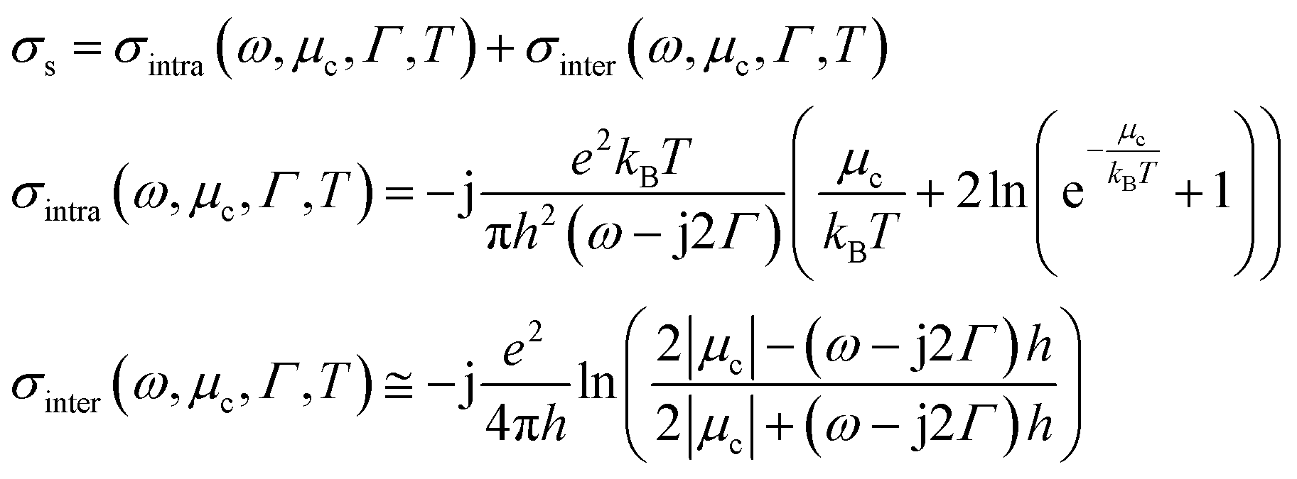
To further reveal the physical mechanisms of the proposed absorber, the field distributions are displayed in Fig. 5, 6 and 7 to reveal the hybridization of the SPP (graphene metasurface) and SSPP (metal metasurface) of the proposed absorber. Note that the fields are obtained under y-polarized incidence. Three peaks at the low (1.62 THz), middle (4 THz) and high (8.05 THz) frequencies of the absorber band are chosen to display the electric and magnetic energy densities. The electric energy density distributions on the graphene metasurface, gold metasurface, xoz-plane and yoz-plane are demonstrated in the subgraphs (a), (b), (c) and (d), respectively. The magnetic energy density distributions on the graphene metasurface, gold metasurface, xoz-plane and yoz-plane are demonstrated in the subgraphs (e), (f), (g) and (h), respectively. | ||
| Fig. 5 Energy density at 1.62 THz. (a), (b), (c) and (d) are the electric energy density of the graphene metasurface, gold (dual rings) metasurface, xoz-plane and yoz-plane, respectively. (e), (f), (g) and (h) are the magnetic energy density of the graphene metasurface, gold metasurface, xoz-plane and yoz-plane, respectively. | ||
 | ||
| Fig. 6 Energy density at 4 THz. (a), (b), (c) and (d) are the electric energy density of the graphene metasurface, gold (dual rings) metasurface, xoz-plane and yoz-plane, respectively. (e), (f), (g) and (h) are the magnetic energy density of the graphene metasurface, gold metasurface, xoz-plane and yoz-plane, respectively. | ||
 | ||
| Fig. 7 Energy density at 8.05 THz. (a), (b), (c) and (d) are the electric energy density of the graphene metasurface, gold (dual rings) metasurface, xoz-plane and yoz-plane, respectively. (e), (f), (g) and (h) are the magnetic energy density of the graphene metasurface, gold metasurface, xoz-plane and yoz-plane, respectively. | ||
As demonstrated in Fig. 5, 6 and 7, both the electric and magnetic energies of 1.62/4/8.05 THz are basically converged on the metasurfaces. It is found from Fig. 5(a), (b), (e), (f) and 6(a), (b), (e), (f) that the electric and magnetic energies of 1.62 THz and 4 THz are concentrated on both the graphene and gold metasurfaces, while it is found that the electric energy of 8.05 THz is mainly concentrated on the graphene metasurface and the magnetic energy is mainly distributed on the gold metasurface from Fig. 7(a), (b), (e), (f). It is also interesting to find from Fig. 5(a), (b), (e), (f) and 6(a), (b), (e), (f) that the electric and magnetic energies of the graphene metasurface gather under the dual-rings. Moreover, the energies on one metasurface also transfer to the other metasurface as displayed in Fig. 5(c), (d), (g), (h), 6(d), (g) and 7(c), (d), (g), (h). Therefore, there are strong couplings between the graphene and the gold metasurfaces, enhancing the SPPs of the graphene and merging the resonances of the metasurfaces. Thus, the energies in the very wide band are trapped in the graphene/gold metasurfaces and dissipated.
Besides, multiple reflections and superpositions between the metasurfaces and the gold layer also contribute to EM wave dissipation.69 From Fig. 5, 6 and 7(c), (d), (g), (h), it is found that there is also some energy transfer between the metasurfaces and the gold layer, and their couplings can't be negligible. Of course, at low-frequencies, the energies are mainly distributed around the gold and graphene metasurfaces, while more energies are transferred to the gold layer at high frequencies as indicated in Fig. 7(c), (d), (g) and (h). This is because Fabry–Perot resonance may occur at high frequency as the thickness h1 is comparable to the wavelength of high frequency. Then, the multiple reflections between the metasurfaces and the gold layer effectively trap EM waves and contribute to wave absorption.
3.3 Discussion
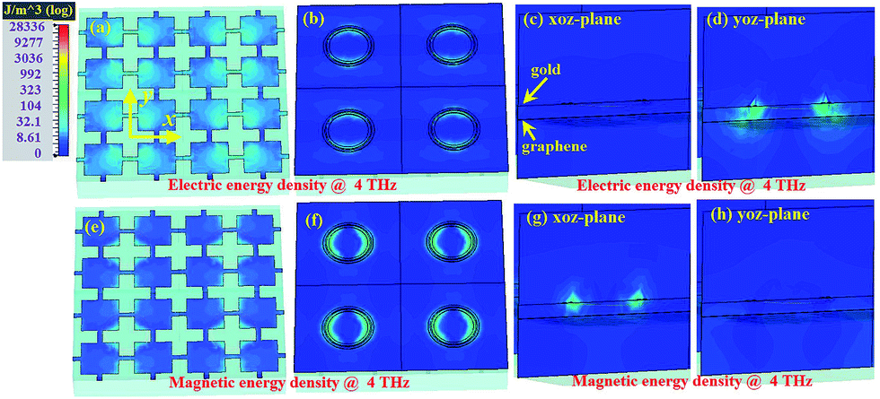
The proposed UWB absorber with metal (gold) and graphene hybridized metasurfaces exhibits robust characteristics that are highly desired in practical applications. To consolidate this conclusion, the absorption characteristics for different thicknesses h1/h2, different polarization angles (Φ), incident angles (θ) and chemical potentials (μc) are investigated in this section.To further verify the discussion in the Section Field distributions, the absorptivity for different substrate thicknesses h1 and h2 is plotted in Fig. 8(a) and (b), respectively. As shown in Fig. 7(a), though the lower edge of the absorption band decreases a little with h1 increasing, it can be concluded that the lower edge is not sensitive to h1. However, the higher frequencies of the absorption band are susceptible to h1. This is coincident with the discussion in paragraph 3 of the section Field distributions, which points out that Fabry–Perot resonance occurs at high frequency. From Fig. 8(b), it is observed that the absorptivity degrades as the distance (h2) between the gold metasurface and graphene metasurface diverges from the proposed value 3 μm. Therefore, this verifies the conclusion in the sections Responses of the metasurfaces and Field distributions that the coupling between the gold metasurface and the graphene metasurface is important for the absorptive characteristics of the proposed absorber.
 | ||
| Fig. 8 The absorption characteristics of the proposed absorber for different thicknesses h1/h2 (a) h1, and (b) h2. | ||
Fig. 9 depicts the absorptivity for different polarization angles (Φ). The Φ is the angle of the incident electric field relative to the y-axis. Note that, as the structure of the absorber is symmetric to x- and y-axes, the Φ changes from 0° to 45°. As shown in the figure, the absorptivity of the proposed UWB absorber is little affected by the polarization angle Φ, and the structure is completely insensitive to the polarization of normal incidence.
 | ||
| Fig. 9 The absorption characteristics of the proposed absorber under normal incidence for different polarization angles (Φ). The Φ is the angle of the incident electric field relative to the y-axis. | ||
The function of the absorption in terms of chemical potentials (μc) is presented in Fig. 10. It is found that the absorption band of the proposed absorber can be further modulated via tuning the chemical potentials (μc) of the graphene metasurface. As exhibited in the figure, the absorption band moves from 0.94–7.68 THz to 1.14–8.46 THz by changing the chemical potentials (μc) from 0.4 eV to 0.7 eV, while the absorptivity is above 0.8. It is also found that the absorptivity in the 5–6 THz band can be adjusted from 0.56 to 0.98 by tuning the chemical potentials (μc) from 0.2 eV to 0.5 eV. Therefore, the amplitude modulation depth in the 5–6 THz band is up to 95.4%. Here, the amplitude modulation depth is calculated by (Prmax − Prmin)/Prmax, where the Prmax and Prmin are the maximal and minimal reflected powers, respectively.
 | ||
| Fig. 10 The absorption characteristics of the proposed absorber for different chemical potentials (μc). | ||
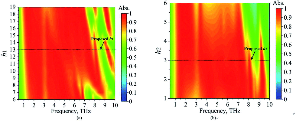
The absorption performances for different incident angles (θ) are presented in Fig. 11. Both the s- and p-polarized waves are illuminated on the structure with their results shown in Fig. 11(a) and (b), respectively. Note that the s-polarization is perpendicular to the incident plane and the p-polarization is parallel to the incident plane, and the incident plane is formed by the normal line of the metasurfaces and the incident line of the wave. As shown in the figures, the absorption functions of the absorber are quite stable as the incident angle θ increased for both s- and p-polarizations. Of course, the s-polarization presents better absorption function than the p-polarization as the incident angle θ increasing. It is found from Fig. 11(a) that the absorptivity of s-polarization is still larger than 0.9 in the band as the incident angle θ increased to 60°, and it is larger than 0.8 as the incident angle θ increased to 68°. For p-polarization illumination as demonstrated in Fig. 11(b), the absorptivity is larger than 0.9 in the band as the incident angle θ increased to 35°, and it is still larger than 0.8 as the incident angle θ increased to 45°. Besides, the bandwidth for s-polarization incidence is quite stable to the incident angle θ, and the increase of θ has a small effect on the high edge of the band. Therefore, the proposed absorber demonstrates good function to the incident angle θ, and it is quite insensitive to the incident angle θ.
 | ||
| Fig. 11 The absorption characteristics of the proposed absorber for different incident angles (θ), illuminated by (a) s-polarized and (b) p-polarized waves. | ||
4 Conclusions
In summary, we proposed a general scheme to design UWB terahertz absorbers by combining metal and graphene metasurfaces. The metal metasurface can increase the SPPs of the graphene metasurface, and its resonances are also coupled with the resonances of the graphene metasurface. These characteristics allow the metal/graphene metasurfaces to achieve a wide absorption band. Moreover, the multiple reflections and superpositions between the metasurfaces and the gold layer further enhance the absorption. Compared to the previous wideband absorbers, our design achieves a much wider bandwidth. The band for absorptivity above 0.9 is 1.24–7.70 THz (6.46 THz, 145%, and octave 6.21), while the band for absorptivity above 0.8 is 1.02–8.26 THz (7.24 THz, 156%, and octave 8.10). Our design may present a new approach to design UWB terahertz absorbers, and find broad applications in terahertz imaging, sensing, photodetection and modulation systems.Conflicts of interest
There are no conflicts to declare.Acknowledgements
This work was supported by the National Natural Science Foundation of China under Grant No. 61661011.Notes and references
- C. M. Watts, X. Liu and W. J. Padilla, Adv. Mater., 2012, 24, OP98–OP120 CAS.
- Y. Cui, Y. He, Y. Jin, F. Ding, L. Yang, Y. Ye, S. Zhong, Y. Lin and S. He, Laser Photonics Rev., 2014, 8, 495–520 CrossRef CAS.
- Z. Xu, D. Wu, Y. Liu, C. Liu, Z. Yu, L. Yu and H. Ye, Nanoscale Res. Lett., 2018, 13, 143 CrossRef PubMed.
- A. Dorodnyy, Y. Salamin, P. Ma, J. V. Plestina, N. Lassaline, D. Mikulik, P. Romero-Gomez, A. F. i. Morral and J. Leuthold, IEEE J. Sel. Top. Quantum Electron., 2018, 24, 4600313 Search PubMed.
- K. Crozier, K. Seo, H. Park, A. Solanki and S.-Q. Li, IEEE J. Sel. Top. Quantum Electron., 2018, 24, 1–7 Search PubMed.
- Z. Wang, R. Wei, J. Gu, H. Liu, C. Liu, C. Luo, J. Kong, Q. Shao, N. Wang and Z. Guo, et al. , Carbon, 2018, 139, 1126–1135 CrossRef CAS.
- B. Zhao, J. Deng, R. Zhang, L. Liang, B. Fan, Z. Bai, G. Shao and C. Park, Eng. Sci., 2018, 3, 5–40 CrossRef.
- L. Wang, H. Qiu, C. Liang, P. Song, Y. Han, Y. Han, J. Gu, J. Kong, D. Pan and Z. Guo, Carbon, 2019, 141, 506–514 CrossRef CAS.
- L. Lv, J. Liu, H. Liu, C. Liu, Y. Lu, K. Sun, R. Fan, N. Wang, N. Lu and Z. Guo, et al. , Eng. Sci., 2018, 2, 26–42 CrossRef.
- C. Wang, V. Murugadoss, J. Kong, Z. He, X. Mai, Q. Shao, Y. Chen, L. Guo, C. Liu and S. Angaiah, et al. , Carbon, 2018, 696–733 CrossRef CAS.
- Z. Guo, P. Xie, F. Dang, B. He, J. Lin, R. Fan, C. Hou, H. Liu, J.-x. Zhang and Y. Ma, J. Mater. Chem. C, 2018, 6, 8812–8822 RSC.
- F. Monticone and A. Alu, Rep. Prog. Phys., 2017, 80, 036401 CrossRef PubMed.
- J. He and Y. Zhang, J. Phys. D: Appl. Phys., 2017, 50, 464004 CrossRef.
- R. Alaee, M. Albooyeh and C. Rockstuhl, J. Phys. D: Appl. Phys., 2017, 50, 503002 CrossRef.
- H. Wu, X. Huang and L. Qian, Eng. Sci., 2018, 2, 111–119 CrossRef.
- C. Cheng, R. Fan, Z. Wang, Q. Shao, X. Guo, P. Xie, Y. Yin, Y. Zhang, L. An and Y. Lei, et al. , Carbon, 2017, 125, 103–112 CrossRef CAS.
- P. Xie, Z. Wang, Z. Zhang, R. Fan, C. Cheng, H. Liu, Y. Liu, T. Li, C. Yan and N. Wang, et al. , J. Mater. Chem. C, 2018, 6, 5239–5249 RSC.
- K. Zhang, G.-H. Li, L.-M. Feng, N. Wang, J. Guo, K. Sun, K.-X. Yu, J.-B. Zeng, T. Li and Z. Guo, et al. , J. Mater. Chem. C, 2017, 5, 9359–9369 RSC.
- C. Cheng, R. Fan, Y. Ren, T. Ding, L. Qian, J. Guo, X. Li, L. An, Y. Lei and Y. Yin, et al. , Nanoscale, 2017, 9, 5779–5787 RSC.
- J. Wang, Z. Shi and X. Wang, Eng. Sci., 2018, 4, 79–86 CrossRef.
- N. Wu, C. Liu, D. Xu, J. Liu, W. Liu, Q. Shao and Z. Guo, ACS Sustainable Chem. Eng., 2018, 6, 12471–12480 CrossRef CAS.
- J. Guo, H. Song, H. Liu, C. Luo, Y. Ren, T. Ding, M. A. Khan, D. P. Young, X. Liu and X. Zhang, et al. , J. Mater. Chem. C, 2017, 5, 5334–5344 RSC.
- X. Zhao, J. Zhang, K. Fan, G. Duan, G. D. Metcalfe, M. Wraback, X. Zhang and R. D. Averitt, Photonics Res., 2016, 4, A16–A21 CrossRef CAS.
- X. Zhao, K. Fan, J. Zhang, H. R. Seren, G. D. Metcalfe, M. Wraback, R. D. Averitt and X. Zhang, Sens. Actuators, A, 2015, 231, 74–80 CrossRef CAS.
- H. R. Seren, G. R. Keiser, L. Cao, J. Zhang, A. C. Strikwerda, K. Fan, G. D. Metcalfe, M. Wraback, X. Zhang and R. D. Averitt, Adv. Opt. Mater, 2014, 2, 1221–1226 CrossRef CAS.
- L. Guo, X. Ma, Y. Zou, R. Zhang, J. Wang and D. Zhang, Opt. Laser Technol., 2018, 98, 247–251 CrossRef CAS.
- N. Landy, C. Bingham, T. Tyler, N. Jokerst, D. Smith and W. Padilla, Phys. Rev. B: Condens. Matter Mater. Phys., 2009, 79, 125104 CrossRef.
- X. Liu, T. Starr, A. F. Starr and W. J. Padilla, Phys. Rev. Lett., 2010, 104, 207403 CrossRef PubMed.
- H. Tao, C. Bingham, A. Strikwerda, D. Pilon, D. Shrekenhamer, N. Landy, K. Fan, X. Zhang, W. Padilla and R. Averitt, Phys. Rev. B: Condens. Matter Mater. Phys., 2008, 78, 241103 CrossRef.
- J. Hao, J. Wang, X. Liu, W. J. Padilla, L. Zhou and M. Qiu, Appl. Phys. Lett., 2010, 96, 251104 CrossRef.
- B.-X. Wang, IEEE J. Sel. Top. Quantum Electron., 2017, 23, 1–7 CAS.
- Q. Xie, G. Dong, B. X. Wang and W. Q. Huang, Nanoscale Res. Lett., 2018, 13, 137 CrossRef PubMed.
- H. R. Seren, J. Zhang, G. R. Keiser, S. J. Maddox, X. Zhao, K. Fan, S. R. Bank, X. Zhang and R. D. Averitt, Light: Sci. Appl., 2016, 5, e16078 CrossRef CAS PubMed.
- H. Lv, Y. Guo, Y. Zhao, H. Zhang, B. Zhang, G. Ji and Z. J. Xu, Carbon, 2016, 110, 130–137 CrossRef CAS.
- P. H. Pham, W. Zhang, N. V. Quach, J. Li, W. Zhou, D. Scarmardo, E. R. Brown and P. J. Burke, Nat. Commun., 2017, 8, 2233 CrossRef PubMed.
- R. Alaee, M. Farhat, C. Rockstuhl and F. Lederer, Opt. Express, 2012, 20, 28017–28024 CrossRef CAS PubMed.
- X. Zou, G. Zheng, J. Cong, L. Xu, Y. Chen and M. Lai, Opt. Lett., 2018, 43, 46–49 CrossRef CAS PubMed.
- R. Xing and S. Jian, Opt. Laser Technol., 2018, 100, 129–132 CrossRef CAS.
- X. Chen, W. Fan and C. Song, Carbon, 2018, 133, 416–422 CrossRef CAS.
- K. Aydin, V. E. Ferry, R. M. Briggs and H. A. Atwater, Nat. Commun., 2011, 2, 517 CrossRef PubMed.
- J. Grant, Y. Ma, S. Saha, A. Khalid and D. R. Cumming, Opt. Lett., 2011, 36, 3476–3478 CrossRef CAS PubMed.
- X. Yin, L. Chen and X. Li, J. Lightwave Technol., 2015, 33, 3704–3710 CAS.
- Y. Cui, K. H. Fung, J. Xu, H. Ma, Y. Jin, S. He and N. X. Fang, Nano Lett., 2012, 12, 1443–1447 CrossRef CAS PubMed.
- A. Andryieuski and A. V. Lavrinenko, Opt. Express, 2013, 21, 9144–9155 CrossRef CAS PubMed.
- N. Mou, S. Sun, H. Dong, S. Dong, Q. He, L. Zhou and L. Zhang, Opt. Express, 2018, 26, 11728–11736 CrossRef CAS PubMed.
- D. Chen, J. Yang, J. Zhang, J. Huang and Z. Zhang, Sci. Rep., 2017, 7, 15836 CrossRef PubMed.
- M. Amin, M. Farhat and H. Bağcı, Opt. Express, 2013, 21, 29938–29948 CrossRef PubMed.
- P.-Y. Chen, M. Farhat and H. Bağcı, Nanotechnology, 2015, 26, 164002 CrossRef PubMed.
- P. Fu, F. Liu, G. J. Ren, F. Su, D. Li and J. Q. Yao, Opt. Commun., 2018, 417, 62–66 CrossRef CAS.
- M. Jablan, H. Buljan and M. Soljačić, Phys. Rev. B: Condens. Matter Mater. Phys., 2009, 80, 245435 CrossRef.
- J. W. You and N. C. Panoiu, Opt. Express, 2018, 26, 1882–1894 CrossRef CAS PubMed.
- G. K. Lim, Z. L. Chen, J. Clark, R. G. Goh, W. H. Ng, H. W. Tan and R. H. Friend, Nat. Photonics, 2011, 5, 554–560 CrossRef CAS.
- F. Bonaccorso, Z. Sun, T. Hasan and A. Ferrari, Nat. Photonics, 2010, 4, 611–622 CrossRef CAS.
- H. H. Tang, T. J. Huang, J. Y. Liu, Y. Tan and P. K. Liu, Sci. Rep., 2017, 7, 46283 CrossRef CAS PubMed.
- Y. Yang, L. Jing, L. Shen, Z. Wang, B. Zheng, H. Wang, E. Li, N.-H. Shen, T. Koschny and C. M. Soukoulis, et al. , NPG Asia Mater., 2017, 9, e428 CrossRef.
- G. W. Hanson, J. Appl. Phys., 2008, 103, 064302 CrossRef.
- L. A. Falkovsky, J. Phys.: Conf. Ser., 2008, 129, 012004 CrossRef.
- G. K. Lim, Z. L. Chen, J. Clark, R. G. Goh, W. H. Ng, H. W. Tan, R. H. Friend, P. K. Ho and L. L. Chua, Nat. Photonics, 2011, 5, 554–560 CrossRef CAS.
- F. Bonaccorso, Z. Sun, T. Hasan and A. C. Ferrari, Nat. Photonics, 2010, 4, 611–622 CrossRef CAS.
- D.-W. Wang, W.-S. Zhao, H. Xie, J. Hu, L. Zhou, W. Chen, P. Gao, J. Ye, Y. Xu and H.-S. Chen, et al. , IEEE Trans. Nanotechnol., 2017, 16, 1132–1137 CAS.
- X. Li, L. Lin, L.-S. Wu, W.-Y. Yin and J.-F. Mao, IEEE Trans. Antennas Propag., 2017, 65, 662–672 Search PubMed.
- M. Esquius-Morote, J. S. Gómez-Dı and J. Perruisseau-Carrier, et al. , IEEE Trans. Terahertz Sci. Technol., 2014, 4, 116–122 Search PubMed.
- H. Tao, A. Strikwerda, K. Fan, C. Bingham, W. Padilla, X. Zhang and R. Averitt, J. Phys. D: Appl. Phys., 2008, 41, 232004 CrossRef.
- H. Yan, X. Li, B. Chandra, G. Tulevski, Y. Wu, M. Freitag, W. Zhu, P. Avouris and F. Xia, Nat. Nanotechnol., 2012, 7, 330 CrossRef CAS PubMed.
- Y. Zhang, Y. Feng, T. Jiang, J. Cao, J. Zhao and B. Zhu, Carbon, 2018, 133, 170–175 CrossRef CAS.
- L. Peng, X. f. Li, X. Jiang and S. m. Li, J. Lightwave Technol., 2018, 36, 4250–4258 CAS.
- C. Menzel, C. Rockstuhl and F. Lederer, Phys. Rev. A: At., Mol., Opt. Phys., 2010, 82, 053811 CrossRef.
- G. He and J. Stiens, Plasmonics, 2017, 15, 1–6 Search PubMed.
- H.-T. Chen, Opt. Express, 2012, 20, 7165–7172 CrossRef PubMed.
| This journal is © The Royal Society of Chemistry 2019 |