
A universal layer-by-layer solution-processing approach for efficient non-fullerene organic solar cells†
Rui
Sun‡
a,
Jing
Guo‡
a,
Chenkai
Sun
b,
Tao
Wang
a,
Zhenghui
Luo
c,
Zhuohan
Zhang
d,
Xuechen
Jiao
*ef,
Weihua
Tang
 *d,
Chuluo
Yang
*cg,
Yongfang
Li
*b and
Jie
Min
*a
*d,
Chuluo
Yang
*cg,
Yongfang
Li
*b and
Jie
Min
*a
aThe Institute for Advanced Studies, Wuhan University, Wuhan 430072, China. E-mail: min.jie@whu.edu.cn
bCAS Research/Education Center for Excellence in Molecular Sciences, CAS Key Laboratory of Organic Solids, Institute of Chemistry, Chinese Academy of Sciences, Beijing 100190, China. E-mail: liyf@iccas.ac.cn
cHubei Key Lab on Organic and Polymeric Optoelectronic Materials, Department of Chemistry, Wuhan University, Wuhan 430072, China. E-mail: clyang@whu.edu.cn
dKey Laboratory of Soft Chemistry and Functional Materials, Ministry of Education, Nanjing University of Science and Technology, Nanjing 210094, China. E-mail: whtang@njust.edu.cn
eDepartment of Materials Science and Engineering, Monash University, Victoria, Australia. E-mail: xuechen.jiao@monash.edu
fAustralian Synchrotron, Clayton, VIC, Australia
gCollege of Materials Science and Engineering, Shenzhen University, Shenzhen, 518060, China
First published on 8th December 2018
Abstract
Layer-by-layer (LbL) solution processing is a cost-effective technology for the large-scale fabrication of organic solar cells (OSCs). In this work, LbL OSCs were fabricated using PTQ10/J71 as donors and ITC6-IC/IDIC/MeIC/ITCPTC/ITIC as non-fullerene acceptors (NFAs) without using orthogonal solvents and appropriate co-solvents. Compared with traditional bulk heterojunction (BHJ) OSCs, the corresponding solution-processed LbL devices exhibited higher or comparable power conversion efficiencies (PCEs), which had the advantages of reduced energy loss, stronger absorption spectra, better vertical phase separation, partially increased charge transport property and charge collection efficiency. Furthermore, taking the J71/ITC6-IC and PTQ10/IDIC LbL systems as examples, we fabricated large-area LbL OSCs using the doctor-blading process, which is closer to the roll-to-roll (R2R) technology. Importantly, both OSCs based on J71/ITC6-IC and PTQ10/IDIC LbL with an active area of 1.00 cm2 demonstrated encouraging PCEs of over 10%, which is the record efficiency for large-area LbL OSCs reported in the literature to date. Our work indicates that the solution-processed LbL approach not only presents good generality and high device performance, but also is a superior alternative to the BHJ method for the initial evaluation of photovoltaic materials and the industrial production of R2R OSCs.
Broader contextAmong the photovoltaic technologies, organic photovoltaics (OPVs) are a key technology for inexpensive and sustainable light-to-energy conversion because they can be processed from solution and deposited on flexible plastic substrates using high throughput roll-to-roll technologies. Great progress has been made over the last few years in the development of highly efficient non-fullerene OPVs with power conversion efficiencies (PCEs) exceeding 14% for single solar cells and 17% for tandem solar cells based on the bulk heterojunction (BHJ) configuration. However, the BHJ architecture is not ideal because optimal nanoscale morphologies are very difficult to realize and are highly sensitive to the processing conditions and material properties. Unlike the BHJ approach, the layer-by-layer (LbL) processing strategy can be used to form pseudo-bilayer configurations in active layers, which are beneficial to the charge transportation and collection at the corresponding electrodes. In this contribution, we demonstrated the high generality of the LbL processing approach using the same selective solvent for improving the efficiency and stability of OPVs. Our results indicated that the LbL approach is a superior alternative to the BHJ technique for the fabrication of solution-processed high performance OSCs. |
1. Introduction
As an essential source of renewable energy for a sustainable future, thin-film organic solar cells (OSCs) have attracted considerable attention in recent years because they present promising advantages, such as light-weight, flexibility, low cost, and facile fabrication from roll-to-roll (R2R) processing.1–4 A schematic mechanism of the photocurrent generation in OSCs consists of the following steps:5–8 (1) absorption of photon to produce excitons in donor and acceptor materials; (2) exciton diffusion to the donor–acceptor interface within its lifetime; (3) excitons (bound electron–hole pairs) on the donor/acceptor interfaces separate into electrons in the acceptor and holes in the donor; (4) the electrons and holes transfer through the acceptor and donor networks to the cathode and anode of the device, respectively; and (5) the charge carriers are collected at the corresponding electrodes. The efficiencies of steps (2)–(4) are closely related to the morphology of the photoactive layers of the OSCs. To achieve efficient exciton dissociation, charge transport, and carrier collection, a bulk heterojunction (BHJ) photoactive layer with a large interfacial area with nanostructured phase separation should be highly suggested. Meanwhile, various strategies, such as mixing solvents, additives, solvent annealing treatment, and thermal annealing process, have been introduced to modify the microstructures and mechanical properties of BHJ films. Thus, the morphology control of the photoactive layer is critical to the photovoltaic performance.Since the first bulk heterojunction (BHJ, see Fig. 1a) OSC was reported by Heeger et al. in 1995,9 the power conversion efficiency (PCE) of BHJ OSCs has gradually improved in the last two decades due to the development of new materials and device architectures, recently reaching over 11% for fullerene-based devices10 and over 14%11 for single solar cells with non-fullerene acceptors (NFAs) as well as over 17% for tandem solar cells.12 The BHJ configuration,13 which is a blend of donor and acceptor materials, provides a larger donor/acceptor interface area and an interpenetrating donor–acceptor (D–A) network morphology for efficient charge separation and transportation.8,14 Meanwhile, BHJ layers can be made thick enough for effective photon absorption, leading to enhanced PCEs in the OSCs.15–18 However, the BHJ architecture is not ideal because the optimal nanoscale morphologies of the BHJ active layer are very difficult to realize and are highly sensitive to processing conditions and material properties.13,19,20 Here, the term optimal nanoscale morphology is used to represent the remarkably interpenetrating bicontinuous morphology with domain sizes on the length scale of 10–20 nm and a large interfacial area as well as suitable vertical phase separation in the BHJ active layer. Besides, the unoptimized bulk morphologies negatively impact the optical and electronic properties of BHJ blends and also influence their carrier dynamics.14,21,22
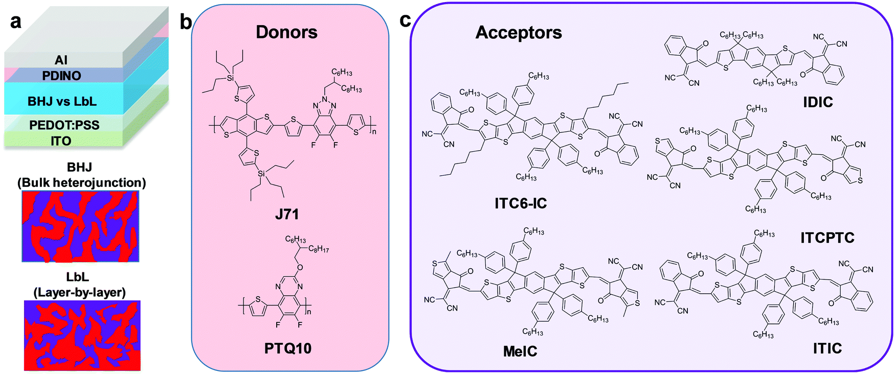 | ||
| Fig. 1 (a) Schematic device architecture of OSCs and the common active layer configurations. Chemical structures of the (b) donor and (c) acceptor materials investigated. | ||
In fact, before the BHJ concept, Tang initially reported a vacuum evaporated bilayer OSC in 1986.23 However, the low exciton dissociation efficiency of the bilayer OSCs limited its development in the past three decades.24,25 To overcome the drawbacks of bilayer devices, as early as 1998, Friend et al. fabricated a D/D:A/A structure (D:A is a mixed blend of donor and acceptor materials) by coating donor and acceptor materials on the corresponding contacts.26 The resulting p–i–n-like structure (D/D:A/A, named layer-by-layer (LbL)) indeed greatly improved exciton dissociation and charge transport. Recently, solution-processed LbL OSCs were investigated in the typical system of poly(3-hexylthiophene) (P3HT)/fullerene derivatives.20,27 For instance, Zhan et al. demonstrated effective solution-processed LbL OSCs fabricated by depositing a PCBM ([6,6]-phenyl C61 butyric acid methyl ester) overlayer on an oligomer donor (BDT-3T-CA) film, which exhibited PCEs of over 4% with excellent fill factor values of up to 0.75.28 Non-fullerene acceptors (NFAs) have also been used in the last two years to construct LbL OSCs.29–31 More recently, Hou et al. employed a specific mixed solvent (o-dichlorobenzene (ODCB)/tetrahydrofuran (THF)) to spin-coat IT-4F onto the polymer donor layer (PBDB-TFS1) via the LbL method for the fabrication of photoactive layers in high-performance OSCs.32 The investigated LbL solar cells exhibited PCEs as high as 13.0%, which is higher than that of their BHJ counterparts (11.8%).
Unlike the solution-processed BHJ approach, LbL processing strategies can form pseudo-bilayer configurations in active layers (such as the p–i–n structure, see Fig. 1a). The proper vertical phase separation can be controlled, which is beneficial for charge transportation and collection at the corresponding electrodes, avoiding the difficulty of controlling the bulk morphology. Also, p–i–n-like bilayer geometries enable easier exciton dissociation at the D–A interface and can reduce charge carrier recombination loss. However, LbL processing needs a set of so-called orthogonal solvents, which allow sequential spin casting of the donor and acceptor layers.19 Considering the special characteristics of the LbL architecture, to date, only a few efforts have been made in developing the LbL strategy due to the lack of successful cases.
In this work, to demonstrate the high generality of the LbL processing approach compared with the BHJ method. We used five different photoactive layer systems, but the same selective solvent (chloroform (CF)) to fabricate LbL OSCs via spin-coating or doctor-blading technology. All five LbL systems exhibited stronger optical absorption and appropriate morphology than the corresponding BHJ OSCs. Also, the LbL systems showed increased carrier mobility and reduced trap-assisted recombination as well as longer carrier drift length in the devices. After simple device optimization, the PCEs of all five LbL OSCs were superior or comparable to that of the corresponding BHJ OSCs. Specifically, the best PCE reached 12.29% for the LbL OSC based on PTQ10:IDIC and 12.08% for the LbL OSC based on J71/ITC6-IC (in comparison with 11.75% and 11.32% for the corresponding BHJ OSCs, respectively). Notably, the LbL OSCs based on the J71/ITC6-IC and PTQ10/IDIC systems, which were fabricated via doctor-blade processing technology in ambient atmosphere, also exhibited high PCEs of over 10% with a device area of 1.00 cm2. These results indicate that the LbL approach is a superior alternative to the BHJ technique for the fabrication of solution-processed high performance OSCs.
2. Results and discussion
2.1 Device performance
The molecular structures of the investigated donor polymers (PTQ1033 and J7134) and the non-fullerene acceptors (IDIC,35 ITC6-IC,36 MeIC,37 ITCPTC,38 and ITIC39) are shown in Fig. 1b and c, respectively. The photovoltaic properties of these five systems were investigated in a conventional device architecture consisting of indium tin oxide (ITO)/poly(3,4-ethylene dioxythiophene):polystyrene sulfonate (PEDOT:PSS)/(donor:acceptor (D:A) for BHJ or D/A for LbL)/PDINO/Al. The complete fabrication of the solution-processed BHJ and LbL OSCs, as well as the thickness control of each layer, are provided in the Experimental section. Fig. 2a presents the average PCEs of the BHJ and LbL OSCs measured under the illumination of an AM 1.5G solar simulator at 100 mW cm−2. The average and best device characteristics of the five BHJ and LbL OSCs are summarized in Table 1. Optimization of the photovoltaic performance of the OSCs was performed by varying the D:A BHJ layer thickness, D/A LbL layer thickness, thermal annealing (TA) conditions and solvent vapor annealing (SVA) conditions. Notably, all of the LbL systems did not need an optimized relative D/A weight ratio, which must be optimized in BHJ devices. The details of the device performance optimization are shown in Fig. S1–S15, and the corresponding photovoltaic parameters are summarized in Tables S1–S15 in the ESI,† respectively.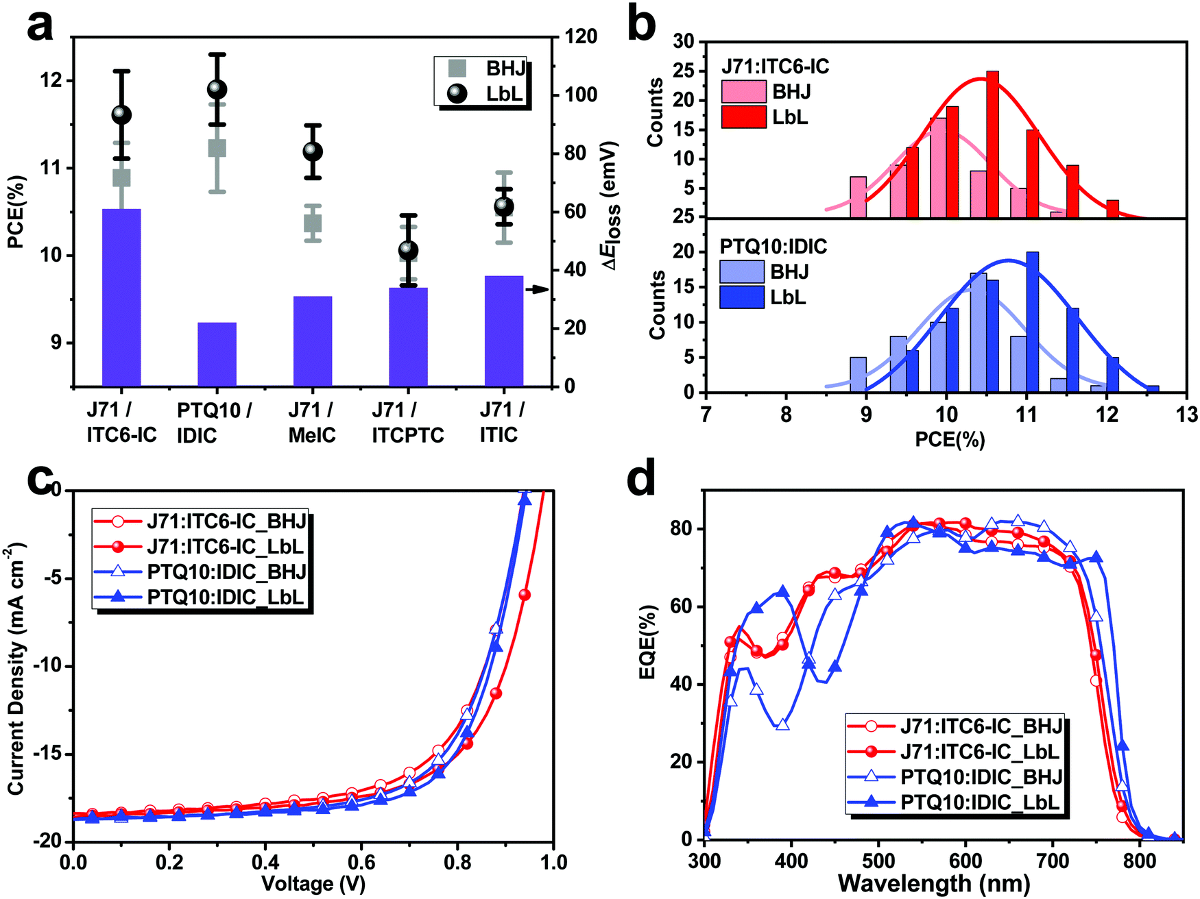 | ||
| Fig. 2 (a) Average PCEs of the BHJ and LbL OSCs and the differences in energy loss between the BHJ and LbL OSCs. Error bars represent plus or minus 1 standard deviation from the arithmetic mean value over six devices. (b) Histogram of PCE counts for the relevant devices. (c) J–V characteristics and (d) EQE spectra of the BHJ and LbL OSCs based on J71:ITC6-IC and PTQ10:IDIC, respectively. | ||
| Active layer | BHJ/LbL | Thickness [nm] | V oc [V] | J sc [mA cm−2] | Calc. Jsca [mA cm−2] | FF [%] | PCE (PCEb) [%] |
|---|---|---|---|---|---|---|---|
| a J sc values calculated from EQE spectra of relevant devices. b The values in parenthesis are the average PCEs obtained from 12 devices. | |||||||
| J71:ITC6-IC | BHJ | 93 | 0.938 | 18.35 | 17.76 | 65.77 | 11.32 (10.89) |
| J71/ITC6-IC | LbL | 64/42 | 0.979 | 18.57 | 17.99 | 66.41 | 12.08 (11.51) |
| PTQ10:IDIC | BHJ | 112 | 0.939 | 18.71 | 17.80 | 66.90 | 11.75 (11.23) |
| PTQ10/IDIC | LbL | 62/44 | 0.943 | 18.75 | 17.99 | 69.66 | 12.32 (11.91) |
| J71:MeIC | BHJ | 103 | 0.908 | 18.37 | 18.06 | 63.37 | 10.57 (10.37) |
| J71/MeIC | LbL | 64/36 | 0.919 | 17.77 | 17.20 | 69.89 | 11.43 (11.19) |
| J71:ITCPTC | BHJ | 90 | 0.881 | 17.46 | 16.92 | 67.96 | 10.46 (10.03) |
| J71/ITCPTC | LbL | 64/50 | 0.909 | 18.21 | 17.39 | 63.07 | 10.44 (10.06) |
| J71:ITIC | BHJ | 102 | 0.930 | 18.06 | 17.21 | 65.75 | 10.95 (10.55) |
| J71/ITIC | LbL | 64/45 | 0.932 | 17.98 | 17.75 | 65.33 | 10.94 (10.47) |
Taking the J71:ITC6-IC system as an example, which has not been reported before, we firstly optimized the thicknesses of the donor and acceptor materials. As shown in Fig. S1 and Table S1 in the ESI,† the PCE of the J71/ITC6-IC OSCs increased first and then decreased with a decrease in the thickness of both J71 and ITC6-IC, and the devices with 64 nm J71/42 nm ITC6-IC LbL layers showed the best photovoltaic performance. Apart from the simultaneous changes in donor and acceptor thickness, we also tried to balance the thickness ratios of the J71 and ITC6-IC thickness by fixing either a thick ITC6-IC layer or a thick J71 layer (see Fig. S2 and S3, ESI†). Furthermore, we kept the same spin-coating speed for each layer and improved the photovoltaic performance via optimization of the heating time and temperature (Fig. S4 and S5, respectively, ESI†). As a result, the optimized PCE of the LbL OSC reached 12.08% (as shown in Table 1), which is higher than that (11.32%) of its corresponding BHJ OSC. Similar with the OSCs based on J71/ITC6-IC, the LbL OSCs based on the J71 donor combed with other NFAs, including MeIC, ITCPTC and ITIC, also showed better or comparable performances than that of the corresponding BHJ OSCs (see Table 1). Specifically, the optimal PCE of the MeIC-based devices increased from 10.57% for the BHJ OSC to 11.43% for the LbL OSC, and the optimal PCE of the ITCPTC- and ITIC-based devices was comparable with that of the corresponding BHJ OSCs. Besides, the optimal PCE of the LbL OSC based on PTQ10/IDIC was 12.32%, which is also higher than that (11.75%, see Table 1) of the corresponding BHJ device. As mentioned above, the LbL OSCs based on J71/ITC6-IC and PTQ10/IDIC exhibited promising PCEs of over 12%, which inspired us to take these two systems as examples to highlight the advantages of the LbL method. Accordingly, the histogram of the PCEs for the BHJ and LbL OSCs based on J71/ITC6-IC and PTQ10/IDIC is presented in Fig. 2b. The PCEs of the LbL J71/ITC6-IC OSCs fluctuated within the range of 9.5% and 12.0%, with an average value of 11.51%. Whereas, the PCEs of the corresponding BHJ devices were in the range of 9.0% to 11.5%, with an average PCE value of 10.89%. Moreover, the PCEs of the LbL PTQ10/IDIC devices were in the range of 9.5% to 12.5%, with an average PCE value of 11.91%; whereas, that of the corresponding BHJ devices were from 9.0% to 12.0%, with an average of 11.23%. The device performance results not only indicate that the LbL approach is a general and universal processing method for material evaluation and device optimization, but also imply that it is possible to improve the performance of ternary OSCs that are currently being studied intensively1,40–42 using the LbL approach.
Compared to the BHJ OSCs (especially for J71/ITC6-IC and PTQ10/IDIC, as exhibited in Fig. 2c), the higher PCEs of the LbL OSCs are attributed to the improved photovoltaic parameters, including Voc, Jsc, and FF. Table 1 shows that the Voc of the LbL devices is slightly higher than that of the BHJ OSCs. Furthermore, combining the optical absorption spectra of the relevant photoactive layers (see Fig. S16, ESI†) and the Voc values of the OSCs (Table 1), we calculated their energy loss (Eloss = Eg − qVoc), as summarized in Table S16 (ESI†). It can be seen that the LbL OSCs exhibited higher Voc and smaller energy loss than that of their corresponding BHJ devices, which is probably due to the larger splitting of the quasi-Fermi levels and somewhat suppression of the charge recombination in the LbL devices.43,44 Also, the slightly higher short-circuit current density (Jsc) and fill factor (FF) values of the LbL OSCs based on J71/ITC6-IC and PTQ10/IDIC should be highlighted. Not surprisingly, the Jsc values for the J71/ITC6-IC and PTQ10/IDIC solar cells are partially consistent with their processing-dependent optical absorption (see Fig. S16 in ESI†). Stronger and slightly red-shifted absorption spectra compared to that of the BHJ layers are one of the inherited advantages of the LbL layers, which probably allow enhanced light capture to be achieved in films. Here, the term light capture is used to mean the successful conversion of absorbed photons into free charge carriers. However, unlike the much different absorption spectra in Fig. S16 (ESI†), the Jsc values of the corresponding BHJ and LbL active layers in this case are comparable, which is mainly due to the different quantum mechanical tunneling. In other words, the light harvesting of the corresponding active layer is mainly determined by the molecular orientation between the donor and acceptor, electron properties of the photovoltaic materials, Förster resonance energy transfer (FRET) distance (LFRET), exciton diffusion length (LD), and interface area of the heterojunction.45 Note that the different optical absorptions observed originate from the altered inter- and intra-molecular conformations of the blend microstructures. This observation is reasonable due to the existence of definite miscibility, which renders the component molecules less ordered in the BHJ film than in the LbL film. As a result, the exciton separation in the LbL systems is not as efficient as that in the BHJ systems, as demonstrated by the PL measurements for both types of systems (Fig. S17, ESI†). Meanwhile it should be highlighted that the enhanced optical absorption of the LbL films gain sufficient excitons without a thick film, indicating that the LbL method may reduce the consumption of expensive photovoltaic materials. The Jsc differences for the J71/ITC6-IC and PTQ10/IDIC OSCs with BHJ and LbL structures were also cross-checked with EQE measurements (see Fig. 2d). The EQE spectra of both LbL systems exhibited slightly broader photocurrent generation, corresponding to the absorption spectra of the active layers, compared to the related BHJ films. The calculated Jsc values from the EQE spectra of the J71/ITC6-IC- and PTQ10/IDIC-based devices are 17.76 mA cm−2 and 17.80 mA cm−2 for the BHJ devices and 17.99 mA cm−2 and 17.90 mA cm−2 for the LbL devices, respectively. The relevant EQE spectra of the other three systems are presented in Fig. S18 (ESI†). Besides, compared to the BHJ devices, the LbL devices exhibited higher FF values, probably because the donor and acceptor materials had more suitable vertical phase separation with continuous pathways for effective hole and electron transport,28 which are confirmed by the morphological characteristics and charge transport properties of the LbL films described in more detail below.
The relationship between layer structure and morphological thermal stability was further studied to complete the potential assessment of this classical LbL structure (see Fig. S19, ESI†). Compared to the LbL devices, the BHJ devices with the exception of the J71:ITC6-IC system exhibited slightly poorer thermal stability. Taking the PTQ10:IDIC system as an example, its performance decreased to 76% of the initial efficiency after annealing for 10 h at 100 °C, while that of the LbL devices decreased to only 90% PCE loss. Overall, the LbL structure seems to positively influence the thermal stability of the heterojunction composite microstructure. Notably, LbL processing generally requires a set of so-called orthogonal solvents, which allow the sequential deposition of the D/A layers.19 In our work, we only used chloroform (CF) as the single processing solvent for the fabrication of all the devices in an inert or ambient atmosphere, which highlights the simple operability and good generality of the LbL technique. As mentioned and discussed above, the improved device performance of the LbL devices without the use of orthogonal solvents or co-solvents also indicates that this LbL processing strategy is more efficient for the fabrication of high-performance OSCs than the BHJ approach, which is probably attributed to their morphological characteristics, as investigated below.
2.2 Morphological characterizations
To clarify the morphological characteristics of the BHJ and LbL layers (specially for J71/ITC6-IC and PTQ10/IDIC), and further understand the fundamental differences in the BHJ and LbL technologies, we applied scanning transmission electron microscopy (TEM), atomic force microscopy (AFM) and synchrotron-based grazing-incidence wide-angle X-ray scattering (GIWAXS) measurements. A cross-sectional TEM image of the J71/ITC6-IC LbL OSC is shown in Fig. 3a. All the individual layers of the device can be clearly distinguished in the TEM image, which had no physical damage. Furthermore, the TEM energy dispersive X-ray spectrometry (EDS) elemental maps (Si, O, and F) of the cross-section confirm a well-organized layer stack. It should be noted that the observed J71/ITC6-IC LbL layer is neither a real bilayer nor pseudo-bilayer without miscibility-induced interdiffusion crossover (a p–i–n-like a bilayer, see Fig. 1a). In fact, interdiffusion of ITC6-IC into the J71 donor layer during the deposition of ITC6-IC resulted in an intermixed heterojunction in the LbL layer, which was caused by the swelling of J71 in the CF solvent used to deposit ITC6-IC. Meanwhile, post-treatment (e.g. thermal annealing) can facilitate the interdiffusion of the donor and acceptor materials. This phenomenon has been reported in polymer/PCBM systems.19 Even though layer mixing between the ITC6-IC layer and the underlying J71 layer was obviously observed, it did not negatively affect the device performance since the LbL layer showed more significant phase separation compared to its BHJ counterpart. Similarly, the TEM images of the cross-section and EDS elemental maps of the PTQ10/IDIC LbL devices showed strong support for the better morphology, as shown in Fig. S20 (ESI†). The AFM surface images of the BHJ and LbL layers (see Fig. 3b and c, respectively, and Fig. S21 in the ESI†) show apparent differences, which can account for the above-mentioned optical absorption differences. Here, the LbL processing approach significantly influenced the film quality with slightly increased surface roughness and obviously enhanced nanoscale phase separation. For example, the surface roughness was 1.003 nm and 1.039 nm for the BHJ and LbL layers of J71/ITC6-IC (see Fig. 3b) and 1.830 nm and 2.034 nm for the BHJ and LbL layers of PTQ10/IDIC (see Fig. 3c), respectively. Besides, the other three systems based on J71 with MeIC, ITCPTC and ITIC acceptors also exhibited a similar trend, where the LbL films exhibited a slightly higher surface roughness and possibly more suitable phase separation (see Fig. S21, ESI†). Although the surface AFM images cannot be directly correlated to the device performance, the microstructure coarsening as a function of the processing approach is consistent with the device performance. Overall, the morphology changes between the BHJ and LbL films in the five systems were not dramatic, but distinct. | ||
| Fig. 3 (a) TEM images of the cross-section and EDS elemental (O, F, and Si) maps. The scale bar is 100 nm. Surface topographic and phase AFM images (size: 5 × 5 μm2) of (b) J71:ITC6-IC BHJ (left: root mean square (RMS) = 1.003 nm) and J71/ITC6-IC LbL (right: RMS = 1.039 nm) films and (c) PTQ10:IDIC BHJ (left: RMS = 1.830 nm) and PTQ10/IDIC LbL (right: RMS = 2.034 nm) films. 2D GIWAXS patterns of (d) J71:ITC6-IC films acquired at the critical incident angle of 0.13° (left: BHJ film and right: LbL film) and (e) PTQ10:IDIC films (left: BHJ film and right: LbL film). 2D GIWAXS patterns of (f) J71:ITC6-IC films acquired at the shallow incident angle of 0.02° (left: BHJ film and right: LbL film) and (g) PTQ10:IDIC films (left: BHJ film and right: LbL film). | ||
To obtain comprehensive information regarding the crystallization and aggregation behavior of the photovoltaic materials within the active layers and demonstrate the different impacts of the BHJ and LbL methods on the thin film morphology, synchrotron-based GIWAXS measurements were further conducted for the J71/ITC6-IC and PTQ10/IDIC LbL films.46 Firstly, the incident angle was chosen at the critical angle to maximize the scattering intensity originating from the active layer and probe the nanostructure across the whole active layer thickness. From the 2D GIWAXS pattern in Fig. S22 (ESI†), both the J71 and PTQ10 donors are revealed to adopt a face-on orientation with respect to the substrate. ITC6-IC acceptor adopts a highly disordered arrangement with weak diffusive scattering from lamellar packing, while the IDIC acceptor adopts a face-on preferential orientation with respect to the substrate. The existence of off-axis diffraction spots suggests the three-dimensional nature of the molecular stacking in the IDIC crystallites. The 2D scattering patterns of J71:ITC6-IC and PTQ10:IDIC processed by the BHJ and LbL methods are presented in Fig. 3d and e, respectively. Intriguingly, the 2D GIWAXS measurements for J71:ITC6-IC revealed distinctly different scattering patterns from the blends processed via the BHJ and LbL methods. Although the J71:ITC6-IC BHJ film generated a 2D scattering pattern highly similar to that of pure J71 (see Fig. S22a, ESI†), the J71/ITC6-IC LbL film displayed an extra sharp Bragg peak located around q = 0.39 Å−1 (d = 16.1 Å) along the in-plane direction and diffusive in-plane lamellar scattering around q = 3 Å−1 (d = 2.09 Å) and out-of-plane scattering around 1.8 Å−1 (d = 3.49 Å). In contrast, the 2D GIWAXS patterns of the PTQ10/IDIC blends processed via the BHJ and LbL methods are highly similar at the critical angle of 0.13°. Both methods induced in-plane lamellar diffraction and out-of-plane π–π diffraction from PTQ10, and in-plane lamellar diffraction from IDIC. Further inspection indicated that the in-plane lamellar diffraction in the PTQ10/IDIC LbL film is sharper than that from the BHJ method (see the comparison of the 1D profiles in Fig. S23, ESI†). These results are in excellent agreement with the film absorption, as mentioned above, and further rationalize the findings from the AFM measurements.
Given the existence of strong vertical phase separation in the LbL-processed films, angle-dependent GIWAXS was performed, which effectively probes various locations along the thin film thickness. The shallow incidence angle of 0.02° was chosen to investigate the crystallization close to the top surface of the organic thin films (see Fig. S24, ESI†). The top layer GIWAXS patterns are shown in Fig. 3f for the J71:ITC6-IC films and Fig. 3g for the PTQ10:IDIC films. Interestingly, the top layer GIWAXS of both blends processed by the LbL method reveals the presence of ITC6-IC or IDIC crystallites, as evidenced by the sharp in-plane lamellar stacking diffraction peaks. In contrast, their BHJ counterparts either showed no such diffraction (e.g., J71:ITC6-IC system) or only displayed negligible scattering (e.g., the PTQ10:IDIC system). This observation unambiguously proves the existence of ordered ITC6IC or IDIC top layers in the LbL layers. Based on the morphological information provided by the angle-dependent GIWAXS measurements, a structure formation and evolution model relevant to the LbL method can be postulated. The observed crystallization phenomena were derived from the competing processes between molecular interdiffusion and molecular aggregation.47 The observed extra sharp Bragg peak from ITC6-IC in the J71:ITC6IC LbL layer at a critical angle is because the molecular aggregation of ITC6-IC proceeds faster than the molecular interdiffusion between ITC6-IC and J71. This fast molecular aggregation leads to the dominant crystallization of ITC6-IC before it drops down to the J71 region and helps maintain the already formed crystallites. On the other hand, the similarity of the 2D GIWAXS in the PTQ10:IDIC layers processed by BHJ and LbL suggest that molecular interdiffusion between PTQ10 and IDIC occurs predominantly faster than molecular aggregation, which highly suppresses the crystallization of IDIC in the LbL layer. Overall, the different morphological formation and evolution based on the same LbL processing strategy further emphasize the universality of this method. Furthermore, the better defined phase separation for both blends with acceptor aggregations also explains the stronger blend absorption (see Fig. S16 in ESI†), and predicts a more efficient charge transport property, as discussed below.
2.3 Physical mechanisms
The variation in the BHJ and LbL morphologies is particularly significant as it changes the interfacial area between the donor and acceptor materials and vertical phase separation as well as defect densities or traps, which, in turn, can cause changes in charge transport and carrier recombination, and therefore impact the device performance.15,21,48,49 To further understand the relationship between charge transport property, composite microstructure, and device performance, we determined the hole mobilities from space charge limited current (SCLC) measurements on representative thin film devices (hole-only devices), as presented in Fig. 4a and Fig. S26 (calculated from Fig. S25 and summarized in Table S17 in the ESI†). Although the LbL devices exhibited better or comparable device performances, it was found that the hole mobility values in the LbL systems were slightly lower than that of the BHJ systems with the exception of the PTQ10:IDIC system. On one hand, the results of the LbL devices based on J71 with four NFAs are not only attributed to their interdiffused structure, but also reflect the existence of an increased acceptor crystallite size on the top of the layers (e.g., ITC6-IC, as illustrated in Fig. 3f). A more unsuitable vertical phase separation with respect to the ITC6-IC crystallites at the top layer probably suppressed the hole transport in the hole-only devices, and thus resulting in poorer hole mobility values in the J71-based LbL devices.41 On the other hand, the comparable mobility values of the PTQ10:IDIC blends processed by BHJ and LbL indicate that the crystallization of IDIC in the LbL blend was highly suppressed due to the faster molecular interdiffusion between PTQ10 and IDIC, as discussed before. | ||
| Fig. 4 (a) Hole-only mobilities measured in single carrier diodes obtained from J71:ITC6-IC and PTQ10:IDIC films. For the SCLC measurements, the values were obtained based on six devices of each type, and the error bars represent plus or minus 1 standard deviation from the mean values (SCLC mobility). Carrier mobilities of both systems calculated from time delayed collection field photo-CELIV (device mobility). (b) Light intensity dependence of Voc and (c) Jsc of the J71:ITC6-IC and PTQ10:IDIC OSCs based on the BHJ and LbL architectures, respectively, together with linear fits to the data (solid lines). (d) Second order recombination coefficient and transient time calculated from the photo-CELIV measurements. | ||
Apart from the SCLC data, we also employed photo-induced charge carrier extraction by linearly increasing the voltage (photo-CELIV) to determine the ambipolar charge extraction from an actual photovoltaic device. To determine the mobility in the devices, photo-CELIV curves were measured using different experimental conditions, differing in delay time and applied voltage. The average mobilities in the devices are provided in Fig. 4a and Fig. S26 (calculated from Fig. S27 and summarized in Table S18 in the ESI†). Importantly, the relevant results did not confirm the mobility trends observed by the SCLC measurements. Here, the average mobility values in the LbL devices, in varying degrees, are higher than that of the BHJ systems (see Fig. 4a and Fig. S26, ESI†). On one hand, this variation in mobility trend may originate from the intrinsic difference between the SCLC model with a hole-only device and the photo-CELIV method for measuring ambipolar charge extraction from an actual photovoltaic device. On the other hand, the variation in the BHJ and LbL blend morphology may also be a factor, and the various vertical phase separations cannot be totally ruled out.
The mobility measurements give great insight into the charge transport properties, but a comprehensive understanding of the differences in photovoltaic parameters in the BHJ and LbL devices requires the acquisition of both the recombination dynamics and transport dynamics. Thus, taking the J71/ITC6-IC and PTQ10/IDIC systems as examples, the relative recombination loss as a function of light intensity was further investigated. The light intensity dependence of the Voc and Jsc of the BHJ and LbL devices based on the J71/ITC6-IC and PTQ10/IDIC systems under various illumination intensities are plotted in Fig. 4b and c, respectively. A stronger dependency of Voc on the light intensity is observed when the additional mechanism of trap-assisted recombination is involved. In this case, if the trap-assisted recombination is significant, the slope of Vocversus light intensity is equal to 2kT/q.50,51 As shown in Fig. 4b, the LbL devices showed slightly less trap-assisted recombination with reduced slopes of 1.24kT/q and 1.29kT/q for the J71/ITC6-IC and PTQ10/IDIC devices (vs. 1.33kT/q and 1.38kT/q for the BHJ solar cells), respectively. This indicates that the trap-assisted recombination is efficiently suppressed in the LbL OSCs compared to the BHJ devices. In addition, the power-law dependence of Jscvs. illumination intensity (Jsc = β(I)α, where α is the exponential factor and β is a constant) can be useful to quantify the bimolecular recombination mechanisms.52Fig. 4c shows the slopes (α values) were 1 for the J71/ITC6-IC and PTQ10/IDIC LbL devices (vs. 0.98 and 0.99 for the BHJ devices, respectively). Importantly, all the devices based on the BHJ and LbL architectures exhibited negligible bimolecular recombination.
To finally understand the recombination dynamics in the relevant devices, photo-CELIV measurements with delayed collection fields were further employed and discussed.50 The initial density of photogenerated carriers (n(0)) and the effective 2nd order recombination coefficient (τB) can be calculated by fitting the corresponding time-dependence of the charge carrier density.50 The τB data is presented in Fig. 4d for the J71/ITC6-IC and PTQ10/IDIC systems and Fig. S28 (ESI†) for the other three J71-based systems. Interestingly, the longer τB indicates that a higher density of trapping states exist in the BHJ devices, which partially confirms the previous recombination dynamics-dependent J–V curves under various light intensities and the related morphological characteristics. Furthermore, we calculated the transient time (ttr) using the formula ttr = d2/μV, where, d is the film thickness.41 The most in-depth insight was gained by analyzing τB in parallel to ttr since both parameters are independent of each other. It was found that the ttr values of the LbL devices are shorter than that of the BHJ devices at a fixed charge density (see Fig. 4d). Also, the shorter charge carrier lifetimes in the LbL devices are consistent with the reduced trapping in the localized states. Apart from the charge carrier lifetime measurements, the higher initial density of photogenerated carriers in the LbL devices compared to that in the corresponding BHJ devices was calculated using the equation n(t) = n(0)/(1 + (t/τB)γ).50 The higher carrier density in the LbL systems mainly results from the reduced recombination loss. Besides, using the equation ld3 = μ2U2e/Jscβ and the known parameters (see Table S18 (ESI†), as measured by photo-CELIV),53 the carrier drift length (ld) was determined. As shown in Fig. S29 (ESI†), the charge carriers, in varying degrees, can travel a longer distance in the LbL blends compared to in the BHJ blends. These findings combined with the higher mobility and reduced trap-assisted recombination in the devices are consistent with the trends of the Jsc and FF values in the relevant devices (especially for the J71/ITC6-IC and PTQ10/IDIC LbL devices). Meanwhile, the results finally support the variation in the BHJ and LbL blend morphology and also give detailed insight into the subtle mechanisms corroborating the link between morphological characteristics and device performance.
2.4 Large-scale LbL OSCs by doctor-blade coating
As discussed above, the photovoltaic performance of the LbL devices based on the five different NFA systems are superior or comparable to that of the corresponding BHJ devices fabricated via spin-coating. Inspired by the results from spin-coating, we diverted our interest to the blade coating of the LbL and BHJ systems with the same device architecture as that used in the spin-coated devices (see Fig. 5 and Fig. S30, ESI†). The blade-coating technique has been widely used to fabricate devices and is proven to be a simple, environment-friendly, and low-cost method for the fabrication of solution-processed R2R OSCs. In our current investigations, we found that one of the critical challenges is to understand the influence of the ambient environment on the resultant blend films and the efficient fabrication of large-area devices. Thus, we investigated the feasibility of achieving LbL and BHJ devices via the blade-coating technique under ambient conditions. | ||
| Fig. 5 Schematic illustration of (a) spin-coating and (b) blade-coating. J–V curves of the blade-coated LbL OSCs with various device areas based on (c) J71/ITC6-IC and (d) PTQ10/IDIC. (e) EQE curves of the blade-coated LbL devices based on J71/ITC6-IC and PTQ10/IDIC. | ||
The film morphology control of the blade-coating method is much simpler than other techniques (e.g., spin-coating, spray coating and R2R printing). Here, high-quality photoactive layers with controllable thickness can be accomplished by adjusting blade speed and substrate temperature, which are some of the critical intrinsic deposition parameters. Fig. 5c and d exhibit the J–V curves of the optimized devices based on the J71/ITC6-IC and PTQ10/IDIC LbLs fabricated via the blade-coating technique. For the devices with an area of 0.04 cm2, both demonstrate excellent performances with a PCE of 11.42% for the J71/ITC6-IC LbL OSC and 11.28% for the PTQ10/IDIC LbL OSC, which are comparable to that of the spin-coated devices. The relevant Jsc values were cross-checked with EQE measurements, as exhibited in Table 2 and Fig. 5e. Furthermore, we manufactured large-area devices with an area of 0.2 cm2 and 1.0 cm2, respectively. As a result of the concomitant defect sites (such as pinholes and fine dust) within the blade-coated films in the fabrication process, the Jsc and FF values generally showed a slight decrease with an increase in the area of the devices. Nevertheless, a high PCE (over 11%) of the device with an area of 0.2 cm2 was still achieved after optimizing the blade-coating process. Impressively, the best performances of the blade-coating LbL devices with an area of 1 cm2 yielded a high PCE of 10.35% for the J71/ITC6-IC OSCs and 10.42% for the PTQ10/IDIC OSCs. Apart from the bladed LbL devices, we also fabricated bladed BHJ devices based on the J71:ITC6-IC and PTQ10:IDIC systems. Compared to the bladed BHJ devices with different device areas (see Fig. S30 and Table S19, ESI†), it was found that the corresponding LbL solar cells also showed better photovoltaic performances. The results suggested that the LbL architecture is a superior alternative to the BHJ structure used in devices with good universality, and also a promising candidate for the large-scale fabrication of high-performance OSCs.
| Active layer | Area [cm2] | V oc [V] | J sc (Jsc_calc.a) [mA cm−2] | FF [%] | PCE (PCEb) [%] |
|---|---|---|---|---|---|
| a J sc values calculated from the EQE spectra of the relevant devices with the active area of 0.04 cm2. b The values in square brackets are the average PCE obtained from 12 devices. | |||||
| J71/ITC6-IC | 0.04 | 0.960 | 17.61 (16.79) | 67.54 | 11.42 (11.25) |
| 0.20 | 0.972 | 17.30 | 66.19 | 11.13 (10.92) | |
| 1.00 | 0.973 | 16.16 | 65.79 | 10.35 (10.24) | |
| PTQ10/IDIC | 0.04 | 0.952 | 17.14 (16.41) | 69.13 | 11.28 (11.01) |
| 0.20 | 0.963 | 16.68 | 69.32 | 11.13 (10.90) | |
| 1.00 | 0.965 | 15.89 | 67.90 | 10.42 (10.18) | |
3. Conclusion
In OSCs, the device performance correlates not only with the degree of mixing but also with the vertical phase separation.3,54 In this work, we applied the LbL processing approach with spin-coating and doctor-blading techniques to fabricate LbL OSCs with five NFA-based photoactive layers. Also, the LbL layers were systematically controlled by choosing a single solvent (CF) during the deposition of the upper layer. Compared to the conventional BHJ devices, the corresponding LbL OSCs not only showed higher or comparable PCEs but also presented enhanced absorption, increased carrier mobility, reduced trap-assisted recombination and slightly reduced energy losses. The optimized PCE of the J71/ITC6-IC LbL OSC reached 12.08%, which is higher than that (11.32%) of its corresponding BHJ OSC. Additionally, the optimal PCE of the LbL OSC based on PTQ10/IDIC was 12.32%, which is also higher than that (11.75%) of its BHJ device. Furthermore, we systematically analyzed the differences in the relevant BHJ and LbL systems with respect to their optical and electronic properties together with the above-mentioned variation in BHJ and LbL morphologies. Then we further fabricated large-area LbL OSCs using the doctor-blading technology and found that the doctor-blading-prepared LbL J71/ITC6-IC and PTQ10/IDIC OSCs with an active area of 1.00 cm2 demonstrated encouraging PCEs of over 10%, which is the record efficiency for LbL solution-processed large-area OSCs reported in the literature to date. The results indicate that the LbL method is an effective way to control the morphology of photovoltaic materials and to fabricate high-performance OSCs, and the LbL processing approach is highly promising for the future industrial production of OSCs.4. Experimental section
4.1 Materials
4.2 Instruments and characterization
4.3 Spin-coated device fabrication and testing
The solar cell devices were fabricated with a conventional structure of Glass/ITO/PEDOT:PSS(40 nm, purchased from Heraeus Holding GmbH)/(donor:acceptor (D:A) for BHJ or D/A for LbL, respectively)/PDINO/Al. Pre-patterned ITO coated glass substrates were purchased from Huananxiangcheng Technology Co. Ltd, Shenzhen. The resistance of the ITO substrates based on a ∼200 nm ITO layer was approximately 15 ohms. These ITO substrates were each washed with methylbenzene, deionized water, acetone, and isopropyl alcohol in an ultrasonic bath for 10 min. After blow-drying by high-purity nitrogen, all the ITO substrates were cleaned in an ultraviolet ozone cleaning system for 15 min. Subsequently, a thin layer of PEDOT: PSS was deposited through spin-coating at 4000 rpm for 30 s on the pre-cleaned ITO-coated glass from a PEDOT:PSS aqueous solution and annealed at 150 °C for 15 min in atmospheric air. The preparation of the relevant solutions was carried out five hours before the deposition of the active layer. The blend solutions consisting of different donors and acceptors in various weight ratios were dissolved at a concentration of 12 mg mL−1 in CF. For the solar cells based on a BHJ structure, the photovoltaic layer was spin-coated in a glovebox from a solution of D:A in chloroform solution (12 mg mL−1) onto the PEDOT:PSS layer at varying spin-coating rates for the different types of BHJ systems. For the photovoltaic devices with the LbL architecture, the donor material in chloroform solution (12 mg mL−1) was spin-coated on the PEDOT:PSS layer to form the front layer, and then a solution of the acceptor (12 mg mL−1) in chloroform was also spin-coated onto the surfaces of the donor layers rotating at different speeds. For the pre-annealing of the donor, after the deposition of the donor layer, the samples were shifted to a glovebox for annealing at different temperatures and times. For the pre-annealing of the LbL film, the active layers were also annealed in the glovebox. To improve the morphology of the LbL film, here we kept the temperature of the baseplate at 45 °C and used different speeds in the range of 10–40 mm s−1. The optimal blade speeds were 30 mm s−1 for the donor layer and 25 mm s−1 for the acceptor layer in the J71/ITIC6-IC and PTQ10/IDIC systems. A Zehntner ZAA2300 automatic applicator was used for the blade-coating of the LbL films. The thickness of the LbL active layer measured by a KLA-Tencor Model 300 profilometer was equal to the total sum of the thickness of every single film of donor and acceptor. Then a methanol solution of PDINO at a concentration of 1.0 mg mL−1 was spin-coated onto the active layer at 3000 rpm for 30 s. To complete the fabrication of the devices, 100 nm of Al was thermally evaporated through a mask under a vacuum of ∼5 × 10⁻⁶ mbar. The active area of the devices was 4 mm2. The devices were encapsulated by glass slides using epoxy in a nitrogen filled glovebox prior to measurement in ambient condition. The current–voltage characteristics of the solar cells were measured under AM 1.5G irradiation on an Enli Solar simulator (100 mW cm−2). Before each test, the solar simulator was calibrated with a standard single-crystal Si solar cell (made by Enli Technology Co., Ltd, Taiwan, and calibrated by The National Institute of Metrology (NIM) of China). The external quantum efficiency (EQE) of the BHJ and LbL organic solar cells were recorded using an Enli QE-R3011 (Enli Technology Co., Ltd Taiwan), and the spectra were calibrated with a single-crystal silicon photovoltaic cell prior to use. Besides, the thicknesses of the thin films were measured using a KLA-Tencor Model 300 profilometer.4.4 Blade-coated device fabrication
The ITO/glass preparation and PEDOT:PSS coating process are consistent with that described for the fabrication of the spin-coated device. The active layer was blade-coated from a chloroform solution with a concentration of 12 mg mL−1 in ambient conditions at room temperature. The blade coating was conducted at different coating speeds for various material systems with a gap of 400 μm between the blade and substrate. The blend morphology was controlled by the blade speed and substrate temperature. Subsequently, the active layers were annealed at different processing conditions. Then methanol solution of PDINO used for spin-coating was spin-coated onto the active layer at 3000 rpm for 30 s. Finally, all the films were completed by thermal evaporation Al (100 nm) under a vacuum of ∼5 × 10⁻⁶ mbar. The active areas of the devices were 0.04 cm2, 0.20 cm2, and 1.00 cm2. The measurements of device performance in these OSCs were the same as mentioned above.Conflicts of interest
There are no conflicts to declare.Acknowledgements
This work was financially supported by the National Natural Science Foundation of China (NSFC) (Grant No. 21702154 and 51773157), the Natural Science Foundation of Hubei Province (Grant No. 2017CFB118) and supported by “the Fundamental Research Funds for the Central Universities (2042017kf0269). This work was performed in part on the SAXS/WAXS beamline at the Australian Synchrotron, part of ANSTO.References
- W. C. Huang, P. Cheng, Y. Yang, G. Li and Y. Yang, Adv. Mater., 2018, 30, 1705706 CrossRef PubMed.
- G. Zhang, J. Zhao, P. C. Y. Chow, K. Jiang, J. Zhang, Z. Zhu, J. Zhang, F. Huang and H. Yan, Chem. Rev., 2018, 118, 3447–3507 CrossRef CAS PubMed.
- F. Zhao, C. Wang and X. Zhan, Adv. Energy Mater., 2018, 8, 1703147 CrossRef.
- P. Cheng, G. Li, X. Zhan and Y. Yang, Nat. Photonics, 2018, 12, 131–142 CrossRef CAS.
- J. Min, X. Jiao, V. Sgobba, B. Kan, T. Heumüller, S. Rechberger, E. Spiecker, D. M. Guldi, X. Wan, Y. Chen, H. Ade and C. J. Brabec, Nano Energy, 2016, 28, 241–249 CrossRef CAS.
- T. Kirchartz, P. Kaienburg and D. Baran, J. Phys. Chem. C, 2018, 122, 5829–5843 CrossRef CAS.
- N. Gasparini, A. Wadsworth, M. Moser, D. Baran, I. McCulloch and C. J. Brabec, Adv. Energy Mater., 2018, 8, 1703298 CrossRef.
- C. M. Proctor, M. Kuik and T.-Q. Nguyen, Prog. Polym. Sci., 2013, 38, 1941–1960 CrossRef CAS.
- G. Yu, J. Gao, J. C. Hummelen, F. Wudl and A. J. Heeger, Science, 1995, 270, 1789 CrossRef CAS.
- H. Chen, Z. Hu, H. Wang, L. Liu, P. Chao, J. Qu, W. Chen, A. Liu and F. He, Joule, 2018, 2, 1–12 CrossRef.
- S. Zhang, Y. Qin, J. Zhu and J. Hou, Adv. Mater., 2018, 30, 1800868 CrossRef PubMed.
- L. X. Meng, Y. Zhang, X. J. Wan, C. Li, X. Zhang, Y. Wang, X. Ke, Z. Xiao, L. Ding, R. Xia, H. Yip, Y. Cao and Y. Chen, Science, 2018, 361, 1094–1098 CrossRef CAS PubMed.
- N. D. Treat and M. L. Chabinyc, Annu. Rev. Phys. Chem., 2014, 65, 59–81 CrossRef CAS PubMed.
- S. Shoaee, M. Stolterfoht and D. Neher, Adv. Energy Mater., 2018, 8, 1703355 CrossRef.
- Y. L. Lin, M. A. Fusella and B. P. Rand, Adv. Energy Mater., 2018, 8, 1702816 CrossRef.
- B. Guo, W. Li, X. Guo, X. Meng, W. Ma, M. Zhang and Y. Li, Adv. Mater., 2017, 29, 1702291 CrossRef PubMed.
- Z. Luo, C. Sun, S. Chen, Z.-G. Zhang, K. Wu, B. Qiu, C. Yang, Y. Li and C. Yang, Adv. Energy Mater., 2018, 8, 1800856 CrossRef.
- D. Li, Z. Xiao, S. Wang, X. Geng, S. Yang, J. Fang, H. Yang and L. Ding, Adv. Energy Mater., 2018, 8, 1800397 CrossRef.
- Y. Wang and X. Zhan, Adv. Energy Mater., 2016, 6, 1600414 CrossRef.
- H. Li and J. Wang, Appl. Phys. Lett., 2012, 101, 263901 CrossRef.
- G. Han, Y. Yi and Z. Shuai, Adv. Energy Mater., 2018, 8, 1702743 CrossRef.
- B. Gautam, E. Klump, X. Yi, I. Constantinou, N. Shewmon, A. Salehi, C. K. Lo, Z. Zheng, J. L. Bredas, K. Gundogdu, J. R. Reynolds and F. So, Adv. Mater., 2018, 30, 1801392 CrossRef PubMed.
- C. W. Tang, Appl. Phys. Lett., 1986, 48, 183–185 CrossRef CAS.
- K. Cnops, B. P. Rand, D. Cheyns, B. Verreet, M. A. Empl and P. Heremans, Nat. Commun., 2014, 5, 3406 CrossRef.
- D. E. Markov, E. Amsterdam, P. W. M. Blom, A. B. Sieval and J. C. Hummelen, J. Phys. Chem. A, 2005, 109, 5266–5274 CrossRef CAS PubMed.
- M. Granström, K. Petritsch, A. C. Arias, A. Lux, M. R. Andersson and R. H. Friend, Nature, 1998, 395, 257 CrossRef.
- A. L. Ayzner, C. J. Tassone, S. H. Tolbert and B. J. Schwartz, J. Phys. Chem. C, 2009, 113, 20050–20060 CrossRef CAS.
- Y. Lin, L. Ma, Y. Li, Y. Liu, D. Zhu and X. Zhan, Adv. Energy Mater., 2014, 4, 1300626 CrossRef.
- K. Tvingstedt, K. Vandewal, A. Gadisa, F. Zhang, J. Manca and O. Inganaes, J. Am. Chem. Soc., 2009, 131, 11819–11824 CrossRef CAS PubMed.
- M. Guide, S. Pla, A. Sharenko, P. Zalar, F. Fernandez-Lazaro, A. Sastre-Santos and T. Q. Nguyen, Phys. Chem. Chem. Phys., 2013, 15, 18894–18899 RSC.
- Y. Wang, X. Zhao and X. Zhan, J. Mater. Chem. C, 2015, 3, 447–452 RSC.
- Y. Cui, S. Zhang, N. Liang, J. Kong, C. Yang, H. Yao, L. Ma and J. Hou, Adv. Mater., 2018, 30, 1802499 CrossRef PubMed.
- C. Sun, H. Bin, J. Zhang, L. Xue, B. Qiu, Z. Wei, Z.-G. Zhang and Y. F. Li, Nat. Commun., 2018, 9, 743 CrossRef PubMed.
- H. Bin, L. Gao, Z.-G. Zhang, Y. Yang, Y. Zhang, C. Zhang, S. Chen, L. Xue, C. Yang, M. Xiao and Y. F. Li, Nat. Commun., 2016, 7, 13651 CrossRef CAS PubMed.
- Y. Lin, F. Zhao, Y. Wu, K. Chen, Y. Xia, G. Li, S. K. K. Prasad, J. Zhu, L. Huo, H. Bin, Z.-G. Zhang, X. Guo, M. Zhang, Y. Sun, F. Gao, Z. Wei, W. Ma, C. Wang, J. Hodgkiss, Z. Bo, O. Inganas, Y. Li and X. Zhan, Adv. Mater., 2017, 29, 1604155 CrossRef PubMed.
- Z. Zhang, J. Yu, X. Yin, Z. Hu, Y. Jiang, J. Sun, J. Zhou, F. Zhang, T. P. Russell, F. Liu and W. Tang, Adv. Funct. Mater., 2018, 28, 1705095 CrossRef.
- Z. Luo, G. Li, W. Gao, K. Wu, Z.-G. Zhang, B. Qiu, H. Bin, L. Xue, F. Liu, Y. Li and C. Yang, J. Mater. Chem. A, 2018, 6, 6874–6881 RSC.
- D. Xie, T. Liu, W. Gao, C. Zhong, L. Huo, Z. Luo, K. Wu, W. Xiong, F. Liu, Y. Sun and C. Yang, Sol. RRL, 2017, 1, 1700044 CrossRef.
- Y. Lin, J. Wang, Z.-G. Zhang, H. Bai, Y. Li, D. Zhu and X. Zhan, Adv. Mater., 2015, 27, 1170–1174 CrossRef CAS PubMed.
- M. Zhang, W. Gao, F. Zhang, Y. Mi, W. Wang, Q. An, J. Wang, X. Ma, J. Miao, Z. Hu, X. Liu, J. Zhang and C. Yang, Energy Environ. Sci., 2018, 11, 841–849 RSC.
- Z. Wang, X. Zhu, J. Zhang, K. Lu, J. Fang, Y. Zhang, Z. Wang, L. Zhu, W. Ma, Z. Shuai and Z. Wei, J. Am. Chem. Soc., 2018, 140, 1549–1556 CrossRef CAS PubMed.
- P. Cheng, R. Wang, J. Zhu, W. Huang, S. Y. Chang, L. Meng, P. Sun, H. W. Cheng, M. Qin, C. Zhu, X. Zhan and Y. Yang, Adv. Mater., 2018, 30, 1705243 CrossRef PubMed.
- N. K. Elumalai and A. Uddin, Energy Environ. Sci., 2016, 9, 391–410 RSC.
- K. Nakano, K. Suzuki, Y. Chen and K. Tajima, Sci. Rep., 2016, 6, 29529 CrossRef CAS PubMed.
- G. J. Hedley, A. Ruseckas and I. D. W. Samuel, Chem. Rev., 2017, 117, 796–837 CrossRef CAS PubMed.
- N. M. Kirby, S. T. Mudie, A. M. Hawley, D. J. Cookson, H. D. T. Mertens, N. Cowieson and V. Samardzic-Boban, J. Appl. Crystallogr., 2013, 46, 1670–1680 CrossRef CAS.
- P. Kohn, Z. Rong, K. H. Scherer, A. Sepe, M. Sommer, P. Müller-Buschbaum, R. H. Friend, U. Steiner and S. Hüttner, Macromolecules, 2013, 46, 4002–4013 CrossRef CAS.
- J. Min, X. Jiao, I. Ata, A. Osvet, T. Ameri, P. Bäuerle, H. Ade and C. J. Brabec, Adv. Energy Mater., 2016, 6, 1502579 CrossRef.
- R. Noriega, Macromol. Rapid Commun., 2018, 39, 1800096 CrossRef PubMed.
- J. Min, Y. N. Luponosov, N. Gasparini, M. Richter, A. V. Bakirov, M. A. Shcherbina, S. N. Chvalun, L. Grodd, S. Grigorian, T. Ameri, S. A. Ponomarenko and C. J. Brabec, Adv. Energy Mater., 2015, 5, 1500386 CrossRef.
- J. Wang, J. Zhang, Y. Xiao, T. Xiao, R. Zhu, C. Yan, Y. Fu, G. Lu, X. Lu, S. R. Marder and X. Zhan, J. Am. Chem. Soc., 2018, 140, 9140–9147 CrossRef CAS PubMed.
- J. Sun, X. Ma, Z. Zhang, J. Yu, J. Zhou, X. Yin, L. Yang, R. Geng, R. Zhu, F. Zhang and W. Tang, Adv. Mater., 2018, 30, 1707150 CrossRef PubMed.
- T. M. Clarke, D. B. Rodovsky, A. A. Herzing, J. Peet, G. Dennler, D. DeLongchamp, C. Lungenschmied and A. J. Mozer, Adv. Energy Mater., 2011, 1, 1062–1067 CrossRef CAS.
- H. Lee, C. Park, D. H. Sin, J. H. Park and K. Cho, Adv. Mater., 2018, 30, 1800453 CrossRef PubMed.
- J. Ilavsky, J. Appl. Crystallogr., 2012, 45, 324–328 CrossRef CAS.
Footnotes |
| † Electronic supplementary information (ESI) available. See DOI: 10.1039/c8ee02560f |
| ‡ The first two authors contributed equally to this paper. |
| This journal is © The Royal Society of Chemistry 2019 |