
 Open Access Article
 This Open Access Article is licensed under a
 Creative Commons Attribution 3.0 Unported Licence
How transport layer properties affect perovskite solar cell performance: insights from a coupled charge transport/ion migration model†
Nicola E.
Courtier
 a,
James M.
Cave
b,
Jamie M.
Foster
c,
Alison B.
Walker
b and
Giles
Richardson
*a
a,
James M.
Cave
b,
Jamie M.
Foster
c,
Alison B.
Walker
b and
Giles
Richardson
*a
aMathematical Sciences, University of Southampton, SO17 1BJ, UK. E-mail: G.Richardson@soton.ac.uk
bDepartment of Physics, University of Bath, BA2 7AY, UK
cDepartment of Mathematics, University of Portsmouth, PO1 3HF, UK
First published on 21st December 2018
Abstract
The effects of transport layers on perovskite solar cell performance, in particular anomalous hysteresis, are investigated. A model for coupled ion vacancy motion and charge transport is formulated and solved in a three-layer planar perovskite solar cell. Its results are used to demonstrate that the replacement of standard transport layer materials (spiro-OMeTAD and TiO2) by materials with lower permittivity and/or doping leads to a shift in the scan rates at which hysteresis is most pronounced to rates higher than those commonly used in experiment. These results provide a cogent explanation for why organic electron transport layers can yield seemingly “hysteresis-free” devices but which nevertheless exhibit hysteresis at low temperature. In these devices the decrease in ion vacancy mobility with temperature compensates for the increase in hysteresis rate with use of low permittivity/doping organic transport layers. Simulations are used to classify features of the current–voltage curves that distinguish between cells in which charge carrier recombination occurs predominantly at the transport layer interfaces and those where it occurs predominantly within the perovskite. These characteristics are supplemented by videos showing how the electric potential, electronic and ionic charge profiles evolve across a planar perovskite solar cell during a current–voltage scan. Design protocols to mitigate the possible effects of high ion vacancy distributions on cell degradation are discussed. Finally, features of the steady-state potential profile for a device held near the maximum power point are used to suggest ways in which interfacial recombination can be reduced, and performance enhanced, via tuning transport layer properties.
Broader contextPerovskite solar cells are an emerging photovoltaic technology that has seen a remarkable rise in power conversion efficiency to above 20% and are the focus of intense research effort. The commercial future of perovskite solar cells is predicted to begin in tandem cells, enhancing the efficiency of the market leader silicon. The physics of standard inorganic solar cells, such as silicon devices, is very well described by drift-diffusion theory. This is not yet the case for metal halide perovskite materials, which display various anomalous current–voltage characteristics. Perovskite solar cell performance is affected by the movement of ions via vacancies in the perovskite structure. This article presents simulation results for a charge transport model that includes both electronic and ionic charge carriers. The use of modelling to predict cell performance is crucial for optimising cell design, in order to obtain the highest efficiencies whilst minimising degradation. This study focusses on how the choice of transport layers affects both transient and steady-state cell performance. We show that, two material properties, namely the majority carrier density and the permittivity, of the transport layers are found to be highly significant in terms of a cell's susceptibility to ion migration and losses via different recombination pathways. |
1 Introduction
Perovskite solar cells (PSCs) have gripped the attention of photovoltaic research groups worldwide due to the rapid rise in their power conversion efficiency (PCE) from 3.8% in 20091 to 22.7% in 2017, certified by the National Renewable Energy Laboratory. In general, the term perovskite describes a class of materials with the chemical formula ABX3; for photovoltaic applications, A is typically an organic cation, B is lead and X a halide. Methylammonium lead tri-iodide (CH3NH3PbI3 or MAPI for short) emerged as the first promising candidate. Alternative perovskite materials employing a wide range of cation–anion mixtures have subsequently emerged, some of which show enhanced stability in comparison to MAPI.2A better understanding of the underlying operating principles of PSCs is required to enable optimisation of their stabilised PCEs via predictive cell design. This understanding is also a crucial step towards combining perovskite technology with existing commercial silicon technologies in tandem architectures. Current–voltage (J–V) hysteresis was first reported by Snaith et al.3 and is now widely understood to be caused by the redistribution of mobile ion vacancies in the perovskite leading to a progressive screening of the perovskite's internal electric field which in turn aids/hinders charge separation.4 While it has been suggested that the motion of methylammonium (MA+) ions is responsible for hysteresis5 it is now generally accepted that the mobile ion vacancy lies on the halide sites (e.g. the iodide sites). This assumption is backed up by the results of carefully designed experiments,6,7 showing the motion of I− ions but not that of MA+ ions over the required timescales, and calculations of the activation energies of ion vacancy motion in the perovskite.8
Recently there has been considerable interest in so-called hysteresis-free cells which exhibit little or no J–V hysteresis at room temperature and at the usual scan-rates (around 10 mV s−1 to 1 V s−1). Experimentally such cells are usually made with organic transport layers (TLs) abutting the perovskite, e.g. PCBM and PEDOT:PSS,9–11 and by ensuring large crystals with few grain boundaries within the perovskite.9,11 Suppressing recombination by passivating interfaces also reduces (or eliminates) hysteresis.10 The sensitivity of hysteresis to the choice of TL materials appears to contradict measurements showing that hysteresis originates in the perovskite layer.3 In particular, Wojciechowski et al.12 show that by replacing the TiO2 TL in a standard cell by a C60 TL the J–V hysteresis can be almost entirely eliminated. Indeed nearly all hysteresis-free cells have organic transport layers. To date, there has been no clear explanation of the sensitivity of hysteresis to choice of TL materials. Another and to date unexplained observation is that by reducing the temperature of a so-called hysteresis-free cell it is possible to observe the re-emergence of J–V hysteresis for scan rates in the standard experimental range.13 Experimental studies are limited by the practical difficulty of altering a single device parameter independently of the others. In contrast, an accurate charge transport model can highlight the roles of individual properties and suggest areas for improvement in a PSC via the minimisation of recombination.
In this work, we explain how properties of the TLs influence cell performance, including the extent of J–V hysteresis, via the mechanism of ion vacancy migration within the perovskite layer. This explanation is provided by solutions to a charge transport model for a planar cell, using parameters appropriate for an absorber layer formed of the most common perovskite material MAPI. We obtain results using a numerical scheme14 uniquely capable of solving a fully-coupled time-dependent drift-diffusion (DD) model for ion vacancy motion and charge carrier transport in realistic parameter regimes. Levine et al.15 and Li et al.16 suggest that different degrees of hysteresis observed for different cell architectures correspond to different activation energies and hence diffusion coefficients. Here, we demonstrate that these differences can instead be explained by variation in the properties of the TLs. We also suggest ways in which vacancy accumulation, which has been linked to chemical degradation at the interfaces,17,18 can be reduced and how the relative importance of bulk versus interfacial recombination can be diagnosed from the shape of a J–V curve.
2 Background
2.1 Experimental findings
In the work of Snaith et al.,3 which first brought to light the issue of J–V hysteresis in PSCs, measurements were made both on standard three-layer planar devices and on two-layer perovskite devices, that lack one or other of the TLs. It was concluded from the two-layer measurements, which show particularly strong hysteresis, that hysteresis arises from an intrinsic property of the perovskite layer, rather than from the TLs or a single interface type, and that the choice of TLs serves to influence the severity of the measured hysteresis.In a similar vein, Xiao et al.19 study a two-layer architecture lacking a hole transport layer (HTL). Their devices exhibit hysteresis, both in the dark and under illumination, and a switchable photocurrent, explained by reversible field-driven ion drift creating either an effective p–i–n or n–i–p homojunction. PSCs with and without a compact TiO2 electron transport layer (ETL) were compared by Zhang et al.20 While both cell architectures can exhibit PCEs >10%, only the cells with a compact TiO2 ETL can maintain this performance when held at maximum power point (MPP). The temporary high PCE of the cell without the TiO2 ETL was attributed to ion motion leading to an accumulation of charge that temporarily enhances efficient charge extraction.
Correa-Baena et al.21 report that replacing TiO2 with a SnO2 ETL improves all-round performance, including reducing the extent of hysteresis. Reduced hysteresis has also been observed for cells employing organic TLs. Shao et al.10 suggest that hysteresis could be eliminated by fullerene passivation of the perovskite/ETL interface. However, Bryant et al.13 show that hysteresis reappears at low temperature for devices with organic TLs (PEDOT:PSS and PCBM). Levine et al.15 confirm this result with a comparison of the extent of hysteresis exhibited by standard-architecture (TiO2/MAPI/spiro) and inverted (PEDOT:PSS/MAPI/PCBM) cells under non-standard measurement conditions that included varying temperature, light intensity and scan rate.
Wolff et al.22 study inverted-architecture PSCs with different fullerene-based ETLs. They conclude that, in terms of improving performance, the suppression of non-radiative recombination holds more importance than energetic alignment across the ETL/perovskite interface. More recently, systematic comparisons of hysteresis in cells with different TL materials and architectures have been made by various authors.23–25 Zimmermann et al.25 emphasize the need to use a reliable, systematic technique to measure PSC performance and suggest such a measurement protocol.
2.2 Modelling progress
The first works to use DD models incorporating ion vacancy motion to explain hysteresis in the J–V curves of PSCs were van Reenen et al.26 and Richardson et al.4 Both are based on a single mobile ion species approximation, assumed to be the iodide ion vacancies. Numerical solution of the appropriate partial differential equations (PDEs) is challenging due to severe spatial and temporal stiffness. In the parameter regimes of interest, the ionic charge accumulates in narrow (∼2 nm) layers, termed Debye layers, adjacent to the interfaces between the perovskite and the TLs. Accurate solution of the PDEs therefore requires a very fine grid spacing local to these internal interfaces in order that the large gradients in electric potential and ionic and charge carrier densities are properly resolved. As a result a high floating-point precision is required to maintain accuracy. The difficulties associated with computing time-dependent solutions is further compounded by the stiffness caused by the large disparity between the timescales of ion vacancy motion and the much faster charge carrier motion.Van Reenen et al.26 qualitatively reproduce trends observed by Tress et al.27 using a finite difference solution method. However, their mesh spacing of ∼4 nm is too coarse to accurately resolve the key physical features resulting from ion vacancy motion, namely the charge distribution across the Debye layers. Additionally, to avoid the temporal stiffness of the problem, they use an ion vacancy mobility that is orders of magnitude greater than that which is commensurate with the observed hysteresis. In order to circumvent the numerical difficulties, Richardson et al.4 use the method of matched asymptotic analysis28 to analyse the problem and are able to produce theoretical results that are close to giving quantitative agreement with their experimental results. Courtier et al.28 show that, by comparing to accurately resolved numerical results, this method, although approximate, still yields very accurate solutions to the problem in the relevant parameter regimes. The same method is used by O'Kane et al.29 to model dark current transients. Domanski et al.30 use a related approach that includes a second, less mobile ion species, assumed to be cation vacancies, to model so-called reversible degradation of PSCs.
Calado et al.31 model three layers of a PSC and show that the combination of ion vacancy motion and recombination near the interfaces between the perovskite and the TLs can explain their experimental results. To avoid the numerical difficulties described above, they made use of a number of simplifying assumptions, such as neglecting the band offsets between the perovskite and TLs (removing the charge selective property of each TL) and incorporating surface recombination at all points within 10 nm of the interfaces.
Other modelling approaches adopted to explain J–V hysteresis include surface polarisation models and doping layer models (DLMs). Ravishankar et al.32 present a surface polarisation model in which a capacitance model for the polarisation of the TL interfaces is coupled to an ohmic resistor used to characterise ion transport in the perovskite. A numerical DLM is presented by Jacobs et al.33 in which ion accumulation is incorporated via narrow “doping” layers adjacent to the interfaces and the magnitude of this doping is determined by the preconditioning; in addition to bulk recombination they find that interfacial recombination is required to reproduce experimental data. A similar application of a DLM model is made by Shen et al.34 to investigate the inverted hysteresis exhibited by some mesoporous PSCs.
More recently, Courtier et al.14 present a high performance numerical method capable of accurately solving the extremely stiff PDEs arising from such DD models. An extension of this method to three layers is used here and allows us to model the effects of the TLs explicitly.
3 Methods
In this section, we: (i) formulate a drift-diffusion model that accounts for both ion vacancy motion and charge transport in the perovskite absorber layer and both TLs of a planar PSC, (ii) justify the chosen parameter values, and (iii) describe the two methods used to obtain solutions. We use the term ‘ion motion’ to refer to the motion of positively charged mobile halide vacancies that are confined to the perovskite layer. The method of solution described in Section 3.3, is the extension of the single-layer (i.e. perovskite layer) tailored numerical scheme presented in Courtier et al.14 to a three-layer structure comprised of the perovskite layer and both TLs. In Section 3.5 an alternative approximate solution method is presented with the goal of improving our understanding of the problem. This method is based on matched asymptotic expansions and, following the work of Richardson et al.4 and Courtier et al.28 leads to a much simplified model that describes the evolution of the five major potential drops across the cell. A particularly significant feature of this approach is the identification of two dimensionless parameters, ΩE and ΩH (defined in (21)), which describe how the potential drops are apportioned between the ETL, perovskite and HTL. All figures in this work are generated using the fully-coupled numerical scheme.3.1 Coupled charge transport ion motion model
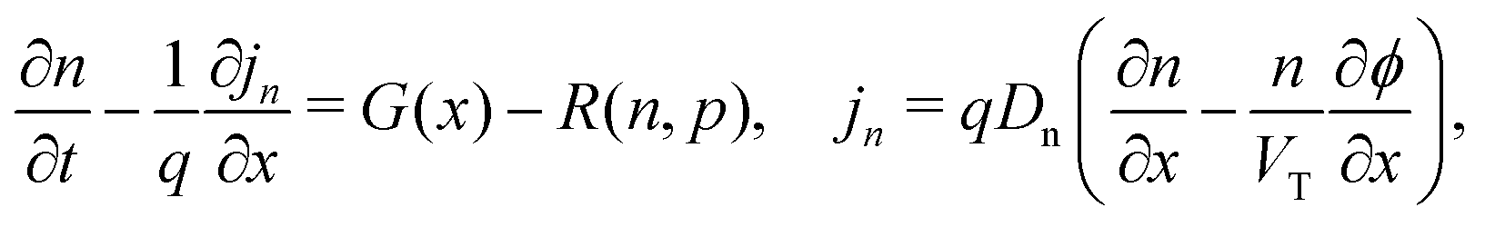
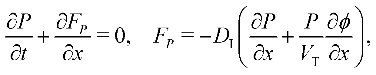
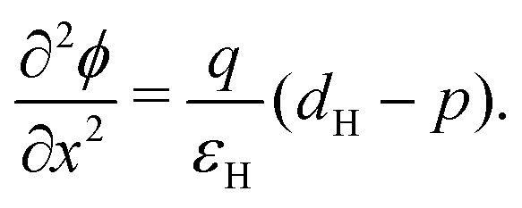
We consider, in one dimension, a planar PSC comprised of an electron transport layer (ETL), perovskite absorber layer and a hole transport layer (HTL) all sandwiched between two metal contacts. Equations describing the conservation of electrons (n, with current jn), holes (p, with current jp) and positively-charged iodide ion vacancies (P, with flux FP) as well as their transport by a combination of thermal excitation (diffusion) and electric field-induced drift are given below. These equations couple to Poisson's equation for the electrostatic potential (ϕ).In the perovskite layer (0 < x < b)
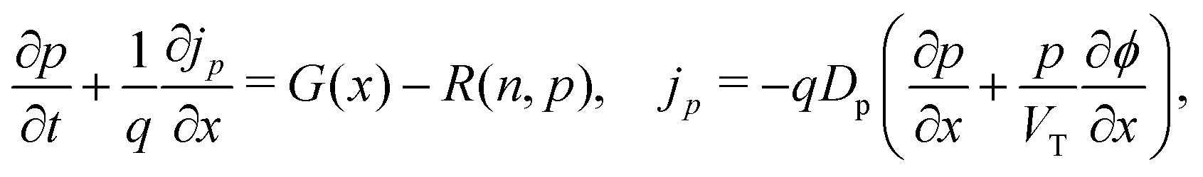 | (1) |
 | (2) |
 | (3) |
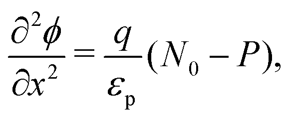 | (4) |
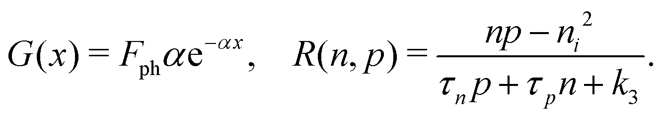 | (5) |
In the ETL −bE < x < 0 conservation of electrons, and Poisson's equation, read
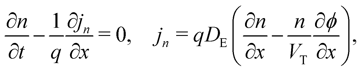 | (6) |
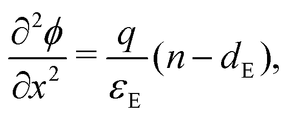 | (7) |
In the HTL b < x < b + bH conservation of holes, and Poisson's equation, read
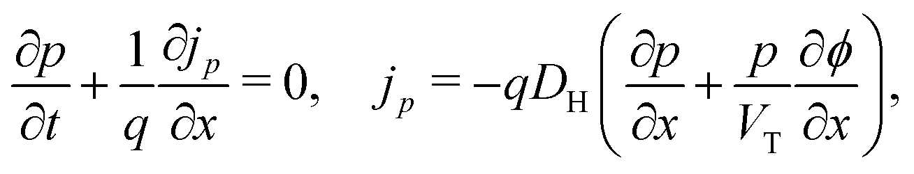 | (8) |
 | (9) |
 | (10) |
 | (11) |
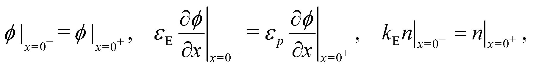
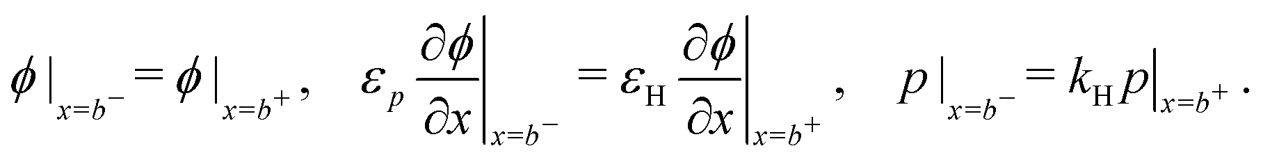
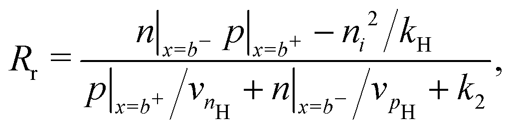
Consistent with precluding the penetration of ions into the blocking layers we impose zero flux of this species on the interfaces and, in addition, impose conditions that allow recombination of the electronic charge carriers across the interfaces. These read
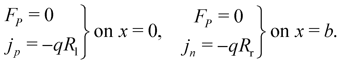 | (12) |
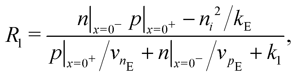 | (13) |
 | (14) |
At the contacts, we impose fixed values of the relevant carrier density35 and a known, time-dependent potential (comprised of the applied voltage Vap(t) and the built-in voltage Vbi):
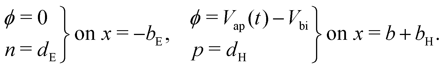 | (15) |
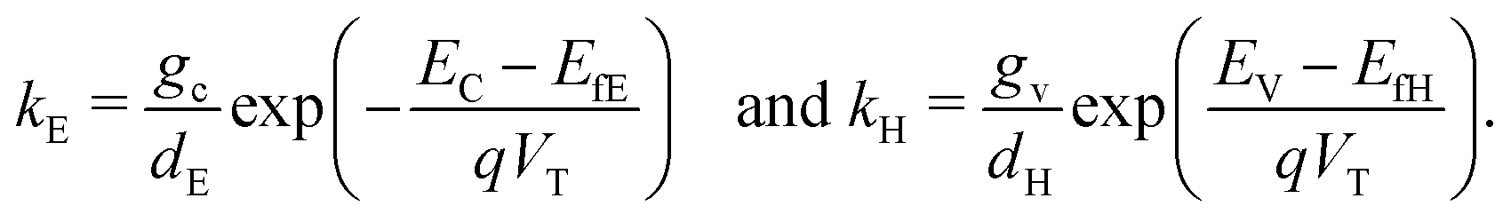
3.2 Choice of parameters
Typical parameter values, listed in Tables 1 and 2, have been chosen in line with the literature and previous work.4,28 The perovskite absorption coefficient, α, is calculated from Loper et al.37 based on a light wavelength of 515 nm, close to the peak absorption of the perovskite layer. We note that Emara et al.38 suggest that the conduction and valence bands of perovskite vary depending on the processing technique.| Sym. | Description | Value | Ref. |
|---|---|---|---|
| q | Charge on a proton | 1.60 × 10⁻¹⁹ C (3s.f.) | |
| T | Temperature | 298 K | |
| V T | Thermal voltage | 25.7 mV (3s.f.) | |
| F ph | Incident photon flux | 1.4 × 10²¹ m−2 s−1 | |
| Perovskite properties | |||
| b | Width | 400 nm | |
| ε p | Permittivity | 24.1ε0 | 39 |
| α | Absorption coefficient | 1.3 × 10⁷ m−1 | 37 |
| E C | Conduction band minimum | −3.7 eV | 40 |
| E V | Valence band maximum | −5.4 eV | 40 |
| D n | Electron diffusion coefficient | 1.7 × 10⁻⁴ m2 s−1 | 41 |
| D p | Hole diffusion coefficient | 1.7 × 10⁻⁴ m2 s−1 | 41 |
| g c | Conduction band DoS | 8.1 × 1024 m−3 | 39 |
| g v | Valence band DoS | 5.8 × 1024 m−3 | 39 |
| N 0 | Density of ion vacancies | 1.6 × 1025 m−3 | 42 |
| D I | Ion vacancy diffusion coefficient | 10−17 m2 s−1 | 4 and 8 |
| ETL properties | |||
| E fE | Fermi level | −4.0 eV | |
| d E | Effective doping density | 5 × 1024 m−3 | |
| b E | Width | 100 nm | |
| ε E | Permittivity | 10ε0 | |
| D E | Electron diffusion coefficient | 10−5 m2 s−1 | |
| HTL properties | |||
| E fH | Fermi level | −5.1 eV | |
| d H | Effective doping density | 5 × 1024 m−3 | |
| b H | Width | 200 nm | |
| ε H | Permittivity | 3ε0 | |
| D H | Hole diffusion coefficient | 10−6 m2 s−1 | |
| Cell property | |||
| V bi | Built-in voltage | 1.1 V | |
| Sym. | Description | Set (a) | Set (b) |
|---|---|---|---|
| τ n | Electron pseudo-lifetime in perovskite | 3 × 10⁻¹¹ s | 3 × 10⁻⁹ s |
| τ p | Hole pseudo-lifetime in perovskite | 3 × 10⁻⁹ s | 3 × 10⁻⁷ s |
| v nE | Electron rec. velocity at ETL interface | 105 ms−1 | 105 ms−1 |
| v pE | Hole rec. velocity at ETL interface | 1 ms−1 | 10 ms−1 |
| v nH | Electron rec. velocity at HTL interface | 0.01 ms−1 | 0.1 ms−1 |
| v pH | Hole rec. velocity at HTL interface | 105 ms−1 | 105 ms−1 |
In this work, we set the diffusion coefficient and density of iodide ion vacancies in the perovskite lattice close to the values predicted from DFT calculations by Eames et al.8 and Walsh et al.,42 respectively. In reality these values depend on the quality of the perovskite morphology, in particular the granularity.
We also keep the widths and band energy levels of each layer the same across all simulations. A schematic band energy diagram for a PSC (in the light) that is initially preconditioned at applied voltage Vap close to Vbi before the applied voltage is suddenly dropped to a value close to zero is shown in Fig. 1. Three types of recombination are included in all simulations with parameters given in Table 2. The values in Set (a) are chosen such that cell performance is limited by bulk recombination, while the cell performance for those in Set (b) is limited by interfacial recombination. For both sets of recombination parameters used here (i.e. for both Set (a) and (b) in Table 2) interfacial recombination on the ETL/perovskite boundary is limited by the perovskite hole concentration and interfacial recombination on the perovskite/HTL boundary is limited by the perovskite electron concentration. That is, (13) and (14) are well-approximated by
| Rl ≈ vpEp|x=0−, Rr ≈ vnHn|x=b−. | (16) |
 | ||
| Fig. 1 A schematic band energy diagram of a PSC (not at steady-state) with dotted lines showing the recombination and generation pathways. Inset: Corresponding potential distribution showing the locations of the 4 Debye layers described by the surface polarisation model. Not to scale. | ||
3.3 Numerical method
The numerical scheme developed by Courtier et al.14 is based on the insights gained from the asymptotic analysis. A non-uniformly spaced grid is used such that points are clustered in the Debye layers adjacent to the interfaces. By packing grid points more tightly at the edges, numerical resolution is provided where it is required without incurring the large computational costs associated with the use of an extremely fine grid across the entire perovskite layer. The stiffness due to the disparity between the timescales of ion vacancy motion and much faster charge carrier motion necessitates the use of fine timesteps. The consequent computational cost can be partially mitigated by implementing an adaptive time-stepping algorithm.14Courtier et al.14 derive finite difference approximations to the spatial derivatives in the equations for ion vacancy motion, charge transport and the electric potential on a staggered grid. This leads to a system of differential algebraic equations (DAEs), rather than ordinary differential equations (ODEs), because Poisson's equation contains no time derivative. The DAEs determining the values of the variables (P, ϕ, n and p) at each of the spatial grid points are then integrated forward in time using the adaptive time-stepping provided by MATLAB's ode15s algorithm, one of few solvers able to cope with systems of DAEs.
Details of the extension of this scheme to include the transport of electrons in the ETL and holes in the HTL are given in the ESI.†
3.4 Hysteresis factor (HF)
In order to quantify the degree of hysteresis exhibited by a particular device for a particular voltage protocol, we define a hysteresis factor as the absolute difference between the area under the forward scan and the area under the reverse scan of a J–V curve, normalised by the area under the reverse scan, see Fig. 2. The formula for the hysteresis factor is therefore | (17) |
 | (18) |
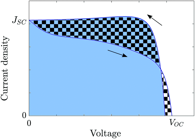 | ||
| Fig. 2 Diagram showing the definition of the hysteresis factor (HF). This is equal to the ratio of the area between the reverse and forward scans (chequered region) to the area below the reverse scan (blue region). | ||
3.5 Asymptotic derivation of a surface polarisation model
Although a numerical method to accurately solve the PDE charge transport model described above has recently been developed,14 a systematic approximation to this model, termed the surface polarisation model, provides much physical insight into the cell's behaviour. In the parameter regime discussed above, approximate (yet highly accurate) solutions to the three-layer DD model (1)–(13) can be generated by using a method based on matched asymptotic expansions. This solution technique is a generalisation of the method described by Courtier et al.,28 used to analyse a single-layer PSC model. As in Courtier et al.,28 the analysis is based on the assumptions that:(i) electronic charge carrier concentrations in the perovskite at illumination of 1 sun are much smaller than the ion vacancy concentration; and,
(ii) the ionic Debye length in the perovskite, defined by 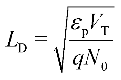 , is much smaller than the width of the perovskite layer.
In the three-layer case, these are augmented by the additional assumptions that:
(i) the Debye length in the HTL, defined by 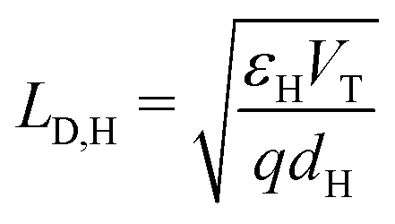 , is much smaller than the width of the HTL;
(ii) the Debye length in the ETL, defined by 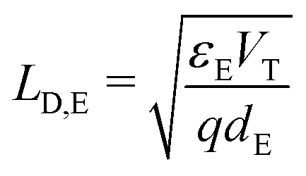 , is much smaller than the width of the ETL; and,
(iii) the timescale for equilibration of the charge carriers in the TLs is much faster than that for the ion vacancies in the perovskite.
Under these conditions it is possible to show the following:
(i) the charge carriers (electrons and holes) in the perovskite layer have such low densities that they do not appreciably affect the electric potential;
(ii) the electric potential profile in the bulk of the perovskite layer is linear, while that in the TLs is flat (except in very narrow Debye layers around the interfaces between the perovskite and TLs, see Fig. 1);
(iii) the ionic charge stored in the Debye layer within the perovskite adjacent to the HTL (density +Q per unit area) is balanced by an equal and opposite charge density (−Q) within the perovskite Debye layer adjacent to the ETL (a consequence of ionic charge conservation in the perovskite layer);
(iv) the ionic charge stored in each of the Debye layers within the perovskite is balanced by an equal and opposite charge in the Debye layer within the adjacent TL; and,
(v) the evolution of the ionic surface charge density Q on the perovskite interfaces is controlled by the flow of ion vacancies from the perovskite bulk into the Debye layers and so is proportional to the bulk electric field Ebulk in the central perovskite region, i.e.
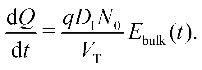 | (19) |
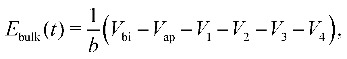 | (20) |
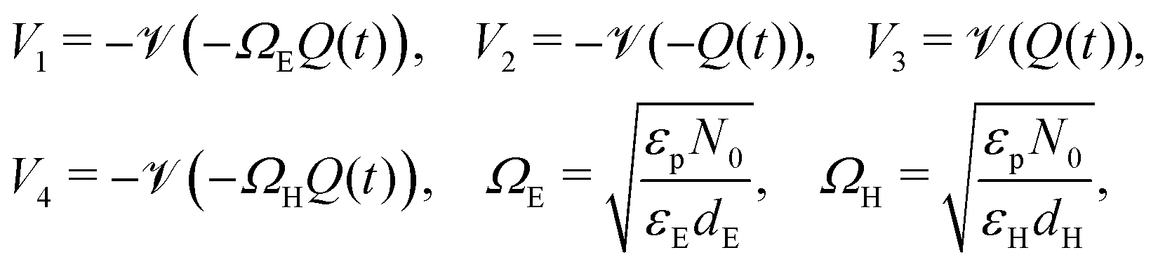 | (21) |
in which the function ![[scr V, script letter V]](https://www.rsc.org/images/entities/char_e149.gif) (Q) is the inverse of the function
(Q) is the inverse of the function
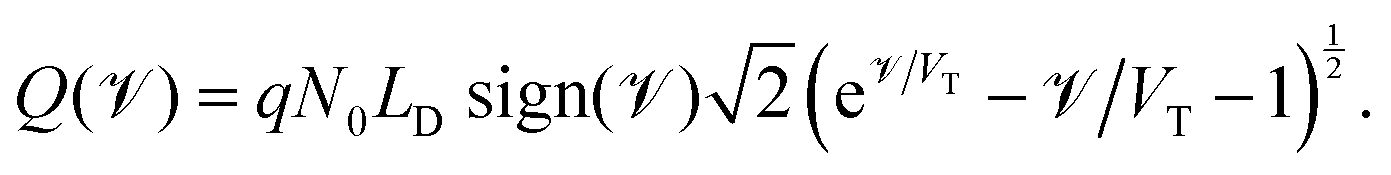 | (22) |
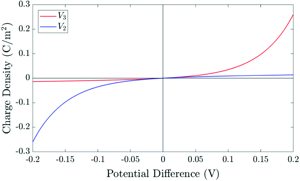 | ||
| Fig. 3 The relationship between the surface charge density (Q) stored within the perovskite Debye layer at the interface with the HTL and the potential differences V2 and V3 across the two perovskite Debye layers, given in (21) and (22). | ||
The simplified asymptotic model comprised of (19)–(22) is termed a surface polarisation model and can readily be solved to determine Q(t), from which the four potential drops V1 − V4 can also be obtained, via(21) and (22). This allows for a complete description of the evolution of the internal electric potential across the three layers of a PSC. A simplified DD model for the charge carriers, based upon this known internal electric potential, may then be solved and used to obtain the cell's J–V characteristics. For further details of this model, which is based on approach (ii) of Courtier et al.,28 see Section B of the ESI.†
The two parameters, ΩE and ΩH, identified in the asymptotic derivation of the surface polarisation model and defined in (21), prove to be key in understanding how the choice of materials for the TLs affect not only the dynamic response of the cell to changes in applied voltage but also its steady-state performance. In particular, they play a key role in determining what proportion of the total potential drop occurs within each Debye layer, i.e. the size of V1 − V4 respectively (see Fig. 1 (inset)). Note that it follows from (21) that the Debye layer potential drops V1 − V4 necessarily take the same sign at any given instant of time. For small values of ΩE (i.e. for an ETL with high doping/permittivity) most of the potential drop across the ETL/perovskite interface occurs inside the perovskite (i.e. |V2| ≫ |V1|) whereas for large values of ΩE most of the potential drop occurs in the ETL (i.e. |V2| ≪ |V1|). Similarly, for small values of ΩH (i.e. for an HTL with high doping/permittivity) most of the potential drop across the perovskite/HTL interface occurs within the perovskite (i.e. |V3| ≫ |V4|) whereas for large ΩH most of this potential drop occurs within the HTL (i.e. |V3| ≪ |V4|). Thus decreasing the product of the permittivity and effective doping density within the transport layers (i.e. εEdE in the ETL and εHdH in the HTL) increases the magnitudes of the potential drop taken up within these layers and decreases the corresponding drops in the perovskite. Thus replacing a TiO2 ETL (high permittivity and doping) with a PCBM ETL (low permittivity and doping) leads to a cell in which less of the potential drop occurs across the perovskite.
3.6 Dependence of recombination losses on the ion distribution
Since the asymptotic model described here provides a very accurate approximation to the full model in the parameter regimes considered here it is sensible (and easier) to discuss recombination losses in terms of this model. As discussed above, the significant disparity between the ion vacancy density (relatively large) and the charge carrier densities (relatively small) means that the electric potential distribution within the cell is set predominantly by the ion vacancy distribution within the perovskite. The key quantities determined by the ion vacancy distribution are the electric field within the perovskite bulk Ebulk and the potential drops V1 to V4 occurring in the Debye layers (see Fig. 1). Where Ebulk > 0 it acts to drive electrons to the ETL and holes to the HTL and thus reduces bulk recombination within the perovskite. In addition positive values of the potential drops V1 and V2 act to drive electrons in the ETL and holes in the perovskite away from the ETL/perovskite interface, respectively, thereby limiting carrier recombination on this interface. While positive values of the potential drops V3 and V4 act to drive electrons in the perovskite and holes in the HTL and away from the perovskite/HTL interface, respectively, limiting carrier recombination at this location. In summary, increasing Ebulk serves to reduce bulk recombination, while increasing V1 and V2 decreases recombination on the ETL/perovskite interface and increasing V3 and V4 decreases recombination on the perovskite/HTL interface (note that these five quantities are related to the applied voltage Vap through (20)). The features of a J–V curve are thus heavily influenced by where the dominant source of recombination is located within the cell.4 Results
The theory of ion vacancy migration explains why hysteresis occurs within a range of scan rates. At low scan rates (i.e. for slow changes to the applied potential), ion vacancy motion is sufficiently fast that the ion vacancy distribution remains close to quasi-equilibrium (i.e. the vacancy electrochemical potential is spatially invariant) and the measured current is therefore almost independent of the scan direction, depending solely on the applied voltage. At high scan rates (i.e. for rapid changes to the applied potential), ion vacancy motion is not fast enough to cause more than minor changes to the initial ion distribution during the scan and so, once again, the measured current is close to being independent of the scan direction. However, at intermediate scan rates, the history of the scan impacts the ion vacancy distribution, and hence also the internal electric fields and the measured current. Under such circumstances the J–V curve is likely to exhibit noticeable hysteresis with marked differences between currents measured (at the same voltage) on the reverse scan from those on the forward scan. Such an example is shown in Fig. 4, for a cell preconditioned at Vap = 1.2 V for 40 seconds then scanned down to Vap = 0 V and back at a scan rate of 75 mV s−1. An animation of the evolution of the ion vacancy, electric potential, electron and hole distributions alongside the current density and electric field can be found in the ESI.† The extent of the J–V hysteresis depends on how the internal potential distribution, resulting from different ion vacancy distributions, affects charge carrier recombination and consequently the current. This will be discussed later but first we consider how the properties of the TLs affect the magnitude of ion vacancy migration.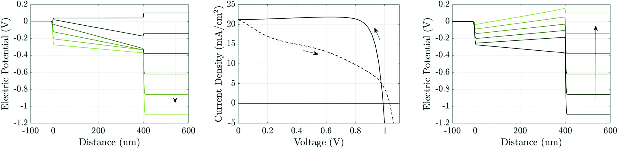 | ||
| Fig. 4 Simulation of a J–V scan at a rate of 75 mV s−1 for a cell with the parameter set in Tables 1 and 2(a), after 40 seconds preconditioning at Vap = 1.2 V. Panel (a) shows potential distributions across the cell at six evenly-spaced times (between and including t = 40 s and t = 56 s) during the reverse scan, shown in panel (b) by the solid line, evolving in the direction of the arrow. Panel (c) shows the potential distributions during the forward scan, shown in panel (b) by the dashed line, at six evenly-spaced times (between and including t = 56 s and t = 72 s). | ||
4.1 Changes to TL properties that reduce ion vacancy migration and affect hysteresis
As discussed above, in Section 3.5, the parameter regimes considered here lead to solutions in which the internal electrical environment of the cell is almost solely determined by the slow motion of ion vacancies within the perovskite layer. In turn this internal electrical environment controls the level of charge carrier recombination and hence the current flow in the cell. We therefore seek first to understand ion vacancy motion, in isolation from the perovskite charge carriers, before looking at its consequences on perovskite charge carrier distributions and the resulting current extracted from the cell.The driving force for ion vacancy migration is the nearly uniform electric field across the bulk of the perovskite layer, as the electronic carrier densities are sufficiently small that they do not appreciably screen the internal electric field. Under the action of this field, electric charge (in the form of ion vacancies) is redistributed between the two perovskite Debye layers which, in turn affects the potential drops across the Debye layers. For a steady applied voltage this leads to a progressive screening of bulk electric field as the potential drop across the cell is progressively absorbed into the Debye layers. These processes are well-described by the approximate surface polarisation model (19)–(21).
Essential to understanding the effects of the TLs on ion vacancy motion are the dimensionless parameters ΩE and ΩH (defined in (21) and discussed in Section 3.5) which encapsulate the key properties of the ETL and HTL, respectively. In Fig. 5, we use the full numerical model to demonstrate that the behaviour of the cell depends on the bulk properties of the TLs almost entirely through these parameters by showing that the HF versus scan rate curves for three cells with different permittivities εE and doping dE, but with fixed ΩE (and ΩH), are almost identical. Here, although the doping and permittivity in the ETL varies between the three cells, the product of these two quantities (dEεE) is fixed and hence so is ΩE. The same level of agreement can be found for an equivalent variation of the HTL parameters, dH and εH (but is not shown here). Furthermore our numerical simulations show that, within the range of parameters considered, TL widths and carrier diffusion coefficients do not significantly alter the cell's properties.
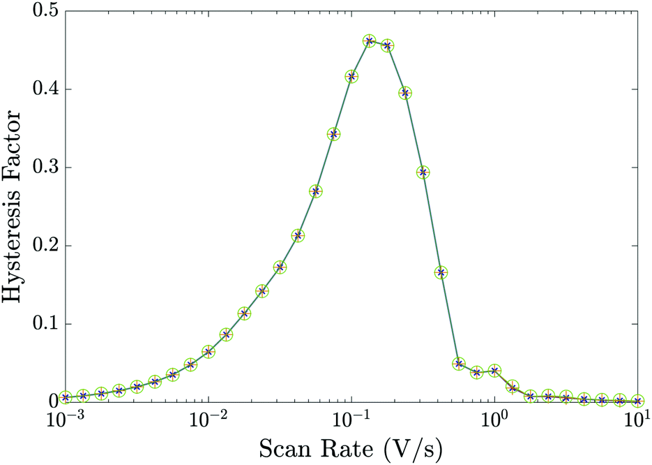 | ||
Fig. 5 Hysteresis factor vs. scan rate for three different sets of the ETL effective doping density dE and permittivity εE that give equal values of ΩE. Precisely,  and εE = [3, 10, 40]ε0 in green circles, orange pluses and blue crosses respectively; all other parameters fixed equal to the values in Tables 1 and 2(a). and εE = [3, 10, 40]ε0 in green circles, orange pluses and blue crosses respectively; all other parameters fixed equal to the values in Tables 1 and 2(a). | ||
The surface charge density–potential relations found in (21b, c) and (22), and plotted in Fig. 3, show that reduced potential drops in the Debye layers lying within the perovskite (i.e. V2 and V3 as shown Fig. 1 (inset)) correspond to a reduced ionic surface charge density Q within the Debye layer.
Fig. 6 shows the effect of varying the permittivity of the ETL (εE), whilst keeping its doping (dE) fixed, on the evolution of the ionic surface charge density Q during the voltage transient plotted in the same figure. This transient starts with a preconditioning step in which the applied voltage is held at the built-in voltage (i.e. Vap = Vbi = 1.1 V), so that initially the Debye layers are uncharged Q = 0, before the voltage is stepped up to Vap = 1.2 V and then reduced in steps to Vap = 0.4 V. Here a permittivity of 3ε0 corresponds to an organic material such as PCBM, while 40ε0 corresponds to a material such as TiO2. The simulations show that lowering the ETL permittivity reduces the magnitude of the Debye layer surface charge density Q throughout the entire transient. We emphasize that almost identical results to those shown in Fig. 6 would be observed if the permittivity εE were held fixed and the value of the ETL doping changed such dE = [1.5, 5, 20] × 1024 m−3 in order to give the same values of ΩE used in the plots.
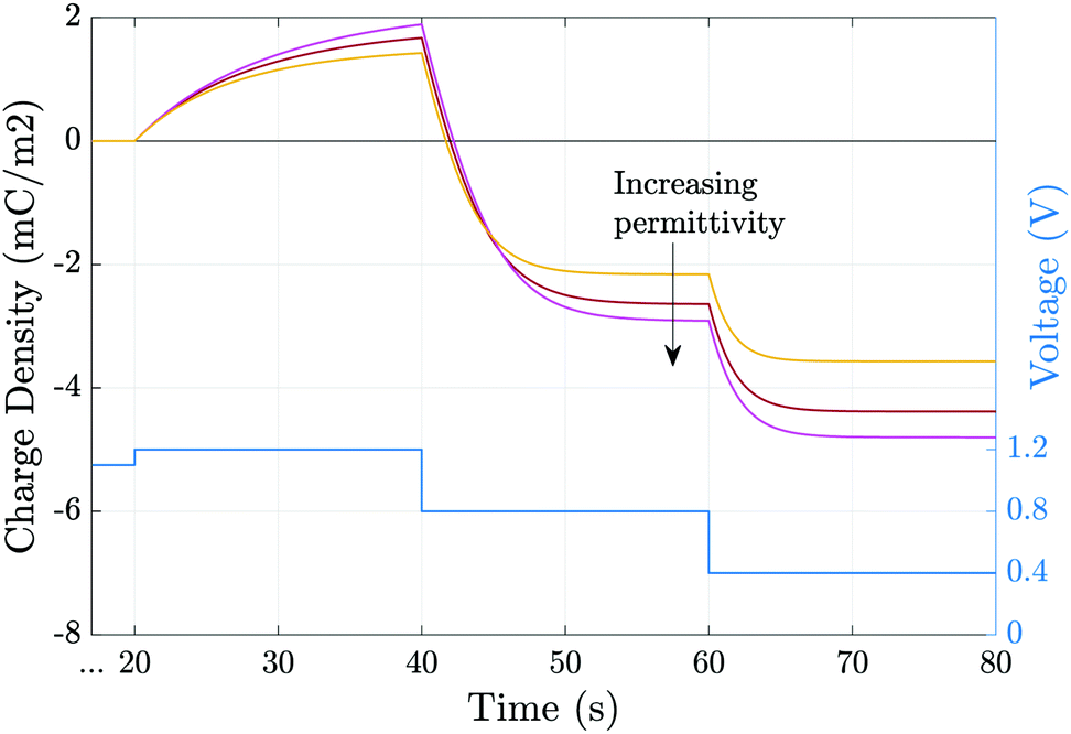 | ||
| Fig. 6 Evolution of the charge density due to the ionic accumulation within ≈10 nm of perovskite adjacent to the ETL during the voltage transient (blue line). Simulations are performed for εE = [3, 10, 40]ε0 while all other parameters remain fixed, as given in Tables 1 and 2(a). | ||
A related effect due to varying both TL doping densities can be seen by comparing Fig. 7(a) and (b) (high TL doping) and Fig. 7(c) and (d) (low TL doping). Here it can be seen that the magnitude of the electric field Ebulk (i.e. minus the gradient of the electric potential) in the perovskite bulk is consistently lower in the low TL doping cell than in the high TL doping cell. This is because in the low TL doping cell a significantly greater fraction of the potential drop across the cell occurs in the TLs (as opposed to across the perovskite) than occurs in the high TL doping cell. These effects can be explained in terms of the dimensionless parameters ΩE and ΩH (introduced in (21)) which apportion the potential drop between the Debye layers in the TLs and the perovskite. In particular ΩE and ΩH are both larger for the low TL doping cell than they are for the high TL doping cell and therefore the potential drops in the TLs of the low TL doping cell are greater than the corresponding potential drops of the high TL doping cell. Notably, the same trends would be observed by comparing devices with high and low permittivity TLs. Notice also that, as expected, in Fig. 7(a) and (b) (high TL doping) most of the potential drop across the Debye layers occurs in the perovskite whereas in Fig. 7(c) and (d) (low TL doping) most of the potential drop across the Debye layers occurs in the TLs. Videos corresponding to similar simulations are included in the ESI.†
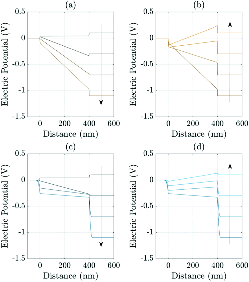 | ||
| Fig. 7 Effects of varying the TL effective doping density on the evolution of the electric potential ϕ. Panels (a) and (b) show the evolution of the potential distributions during the reverse and forward scans, respectively (arrows indicate increasing time) during a 178 mV s−1J–V scan from Vap = 1.2 V to 0 V (reverse scan) and back up (forward scan) for high TL doping (dH = dE = 5 × 1025 m−3). Panels (c) (reverse scan) and (d) (forward scan) shows the evolution of the potential for an almost identical cell but here with low TL doping (dH = dE = 5 × 10²³ m−3). In all panels the other device parameters are given in Tables 1 and 2 Set (a). | ||
The plots of HF versus scan rate made in Fig. 8 demonstrate how observable J–V hysteresis varies with scan rate for different devices, all with significant bulk recombination (using the recombination parameters given in Set (a) of Table 2), but with different TL doping levels. For the lowest TL doping (5 × 10²¹ m−3), the maximum HF is approximately 0.15. As the TL doping levels are increased, the maximum HF reaches over 0.4 and also shifts to lower (measurable) scan rates. The small value of the maximum HF for low TL doping is a result of screening of the electric field from the perovskite by the TLs. Thus, for a cell with low TL doping, the strength of the electric field within the perovskite is decreased, in comparison to a cell with high TL doping. Furthermore, if the predominant loss mechanism is bulk recombination within the perovskite, the differences between the current on the reverse and forward scans of a J–V curve (and consequently the HF factor) are smaller for a cell with low TL doping than they are for a cell with high TL doping.‡ The shift to higher scan rates, as TL doping is decreased, results from a decrease in the size of the surface charge density Q stored in the Debye layers as TL doping is decreased (comparable to the trend shown in Fig. 6). It follows that the scan rate at which maximum hysteresis occurs increases as the TL doping is decreased (indeed the whole curve shifts to the right), as less charge needs to be moved in and out of the Debye layers in order to re-equilibrate the ion distribution. We note that similar trends in HF versus scan rate would be observed if rather than increasing the doping levels, the permittivity were increased instead, since the key quantities encapsulating the electrical properties of the transport layers are ΩE and ΩH.
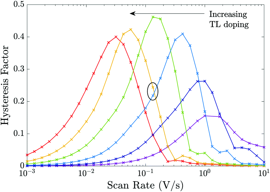 | ||
| Fig. 8 Effects of varying the TL effective doping density on the HF of the cell showing the results for 6 different TL doping densities dH = dE = 5 × [1021, 1022, 1023, 1024, 1025, 1026] m−3 but otherwise using the device parameters in Tables 1 and 2 Set (a) (i.e. except for the TL doping equivalent to the parameters in Fig. 7). | ||
In Fig. 9 we perform a similar investigation of the effects of TL doping on J–V hysteresis to that performed in Fig. 8 except on a device that is limited by interfacial (rather than bulk) recombination by taking the recombination parameters from Table 2 Set (b). Notably, some features of the trends in the HF curves differ from the cell with dominant bulk recombination. In particular, for a device limited by interfacial recombination (Fig. 9), the photocurrent displays a stronger dependence on the potential drops across the interfacial Debye layers than the bulk electric field. As noted in Section 3.6 large positive potential drops (i.e. V1 − V4) across these Debye layers efficiently extract electrons to the ETL and holes to the HTL while opposing the motion of holes onto the ETL/perovskite interface and electrons onto the perovskite/HTL interface, where they can recombine in interfacial traps. Thus, in cells dominated by interfacial recombination the division of the potential drop between the Debye layers at the ETL/perovskite interface and between those at the perovskite/HTL interface (i.e. between V1, V2, V3 and V4) and the location of the predominant recombination pathway play an important role in determining the degree of hysteresis and the overall level of recombination.§
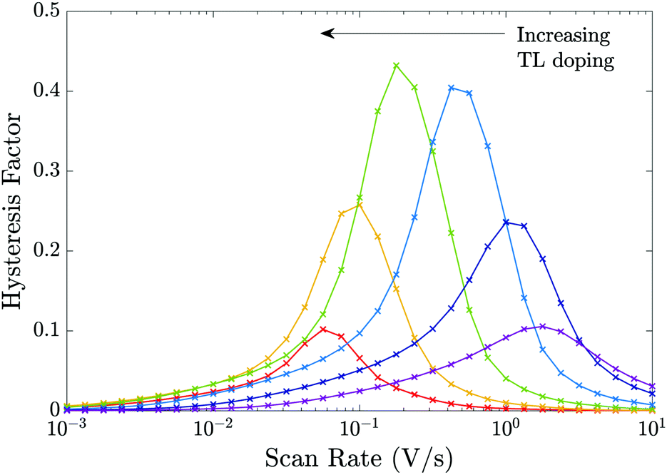 | ||
| Fig. 9 Equivalent to Fig. 8 but for the recombination parameters in Table 2 Set (b), i.e. for a cell limited by recombination at the interfaces. | ||
One notable difference between the sets of HF curves shown in Fig. 8 and those in Fig. 9 occurs as the effective doping density is increased beyond dE = dH = 5 × 1024 m−3 at which HF is most pronounced (green curve). In the former case (predominant bulk recombination) the maximum HF remains relatively high even as the TL doping is increased beyond dE = dH = 5 × 1024 m−3 while in the latter case (predominant interfacial recombination) it decays rapidly from its maximum value as the TL doping is increased beyond dE = dH = 5 × 1024 m−3. The rapid decay in HF with increases in doping, for the predominant interfacial recombination case, can be explained by the fact that as doping increases so the potential drops in the Debye layers within the perovskite (V2 and V3) increase (with respect to the other potential drops) and this is enough to almost eliminate interfacial recombination for all applied voltages much below Vbi, and in turn this reduces the variations that give rise to hysteresis.
The differences resulting from changes to the recombination parameters highlight the importance of also understanding the dependence of hysteresis on the recombination mechanisms within a particular PSC. This aspect is discussed in the next section.
The trend of HF curves being shifted to higher scan rates for cells with lower TL doping densities (shown in both Fig. 8 and 9) or lower permittivities (not shown) is consistent with the reports of low temperature hysteresis for cells with organic TLs made by Bryant et al.13 and Levine et al.15 At room temperature, the hysteresis is present but only for scan rates much faster than commonly used in practice. At lower temperatures, the diffusion coefficient of the ion vacancies is reduced and so the HF curves are shifted back to the scan rates which are commonly probed experimentally. This explains why devices that appear hysteresis-free at room temperature demonstrate hysteresis upon cooling.
Perovskite degradation has been linked to photo-induced formation of superoxide species from oxygen, mediated by iodide vacancies.17,18 The packing of iodide vacancies at the edges of the perovskite, in the form of the Debye layers is likely to aid the diffusion of atmospheric oxygen into the perovskite film, and therefore contribute significantly towards degradation. Hence it is worth noting that increasing ΩE and/or ΩH results in smaller ionic charge densities Q in the perovskite Debye layers at steady-state and during J–V scans (as in Fig. 6). Thus, PSCs with TLs that have low permittivities and/or low doping densities, and consequently reduced ion vacancy accumulation at the interfaces, might be expected to show reduced degradation and longer lifetimes.
4.2 Detecting the dominant recombination mechanism
The aim of this section is use the numerical model to consider how different recombination mechanisms affect the J–V hysteresis. The eventual goal of such a study is to develop tools that can be used to assess the type and location of recombination losses. Since these losses depend on the quality of the perovskite crystal structure and the interfacial contacts, such studies have the potential to guide future cell development and as a tool to assess cell degradation. Here, for simplicity, we vary only the material parameters associated with electronic charge carrier recombination but otherwise set the material parameters equal to those in Table 1. Thus each simulated cell has an identical predisposition for ion vacancy migration. A common feature of all the simulations that we have performed is that reducing the amount of recombination taking place, via any recombination pathway, improves the performance on both forward and reverse scans, and hence reduces the degree of hysteresis.In order to illustrate that the features of the J–V hysteresis can be used to diagnose the dominant recombination pathway we show J–V curves for two representative cells. The first cell, whose J–V curves are shown in Fig. 10(a), has recombination parameters taken from Set (a) of Table 2 and losses that are dominated by bulk recombination. The second cell, whose J–V curves are shown in see Fig. 10(c), has recombination parameters taken from Set (b) Table 2 and losses that are dominated by interfacial recombination. The experimental protocol for both sets of J–V curves, Fig. 10(a)–(c), is as follows: the device is preconditioned at 1.2 V for 40 seconds, the voltage is then scanned down to 0 V at a scan rate of 20 mV s−1 and immediately back up to 1.2 V. The same procedure of preconditioning for 40 seconds and then scanning is then repeated for two more scan rates: 60 mV s−1 and 100 mV s−1.
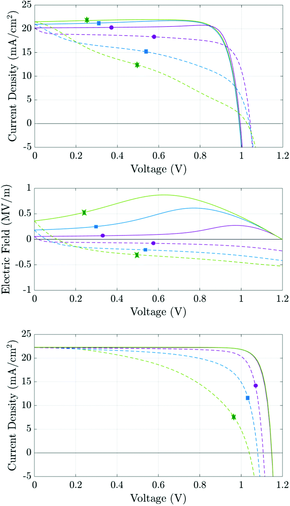 | ||
| Fig. 10 Simulations based on the parameter set in Table 1. Panels (a) and (c) show simulated J–V curves at scan rates of 20 mV s−1 (purple, circles), 60 mV s−1 (blue, squares) and 100 mV s−1 (green, stars) for the recombination parameters given in Table 2 columns (a) and (b), respectively. Solid lines represent the initial reverse scans; dashed lines the subsequent forward scans. Panel (b) shows the electric field at x = 200 nm during the J–V scans. | ||
The first distinct feature is the current maximum (or ‘bump’) on the reverse scans of the two slower J–V curves in Fig. 10(a). This feature arises because, as the scan progresses from high applied voltage to low applied voltage, the charging of the Debye layers lags behind the voltage drop across the cell resulting in a positive bulk electric field Ebulk which, as the scan proceeds, eventually reaches a maximum at Vap ≈ 0.75 V for the medium scan rate (blue curve) before slowly decreasing until Vap = 0 V (see Fig. 10(b)). Where the predominant recombination pathway is bulk recombination within the perovskite the positive electric field serves to separate electronic charge carriers to their respective contacts and thereby reduce recombination losses. The maximum in the current is thus associated with the maximum in Ebulk and the corresponding minimum in bulk recombination. In turn such a maximum in the current on the reverse scan of a J–V curve is a sign of significant bulk recombination.
Another feature which can be attributed to bulk recombination is that of a noticeable drop-off in current just after the switch in scan direction at short-circuit. This drop in current is associated with the steep decrease in Ebulk (see Fig. 10(b)) on a slow to mid-rate scan immediately after the reverse in scan direction.
Near open-circuit (Voc), the potential drops across the Debye layers are relatively small but still crucial for interpreting the different behaviour demonstrated by Fig. 10(a) and (c). At the start of the reverse scan, the drops (V1 − V4) are all negative, because the cell is preconditioned above Vbi (but change sign as the reverse scan proceeds and Vap drops much below Vbi). Negative potential drops V1 + V2 and V3 + V4 across the ETL/perovskite and perovskite/HTL interfacial Debye layers, respectively, act to drive electrons from the ETL, and holes from the HTL, into the perovskite. This substantially increases the magnitude of recombination losses in the perovskite layer to the extent that these swamp the generated current. This effect is particularly pronounced in cells with large numbers of recombination sites in the perovskite layer, such as the one whose parameters are given by Set (a) of Table 1. In turn this explains why such cells, when preconditioned above Vbi, show an effective Voc on the reverse scan that is significantly depressed, often significantly below Vbi. This behaviour is depicted in Fig. 10(a) (for the cell with parameters in Set (a) of Table 1) and results in the crossing of the forward and reverse scan J–V curves. Notably for a cell with significantly smaller numbers of recombination sites in the perovskite layer (with parameters taken from Set (b) of Table 1) the effective Voc on the reverse scan is not significantly depressed, despite the increase in carrier concentrations in the perovskite layer from leakage in from the TLs, and consequently the forward and reverse scan J–V curves do not cross (see Fig. 10(c)).
4.3 Improving steady-state performance
We have demonstrated that varying the parameters ΩE and/or ΩH (by adjusting either the TL doping densities or permittivities) will change the distribution of the electric potential within a PSC during transient measurements. However, the key property of a PSC, its PCE, is measured under steady-state conditions. In this final section, we suggest how the TL doping density (or equivalently permittivity) can be tuned to improve the steady-state photocurrent, for a given density of surface trap states (i.e. fixed recombination velocities). We find that although lower doping densities help to reduce hysteresis, this does not necessarily improve the steady-state performance. We reiterate that the results of Fig. 5 strongly suggest that any benefits that can be achieved by tuning the TL doping levels can similarly be achieved by altering the TL permittivities appropriately, because it is the value of the parameters ΩE and ΩH (defined in (21)) that determine the device's internal potential distribution. Thus, where trends due to raising/lowering the amount of doping are discussed, we could equally discuss the same trends due to an increase/decrease in the TL permittivities.At steady-state, charge is distributed so that the field has been screened throughout the PSC except in the narrow Debye layers about the interfaces. Consequently, at steady-state, the bulk electric field is flat (Ebulk = 0) and the electric potential is split between the four Debye layers. Fig. 11(a) shows three possible steady-state potential distributions for three different pairs of TL doping densities (dE and dH) for cells run near maximum power point (MPP) with Vap = 0.9 V (i.e. Vap = Vbi −0.2 V).
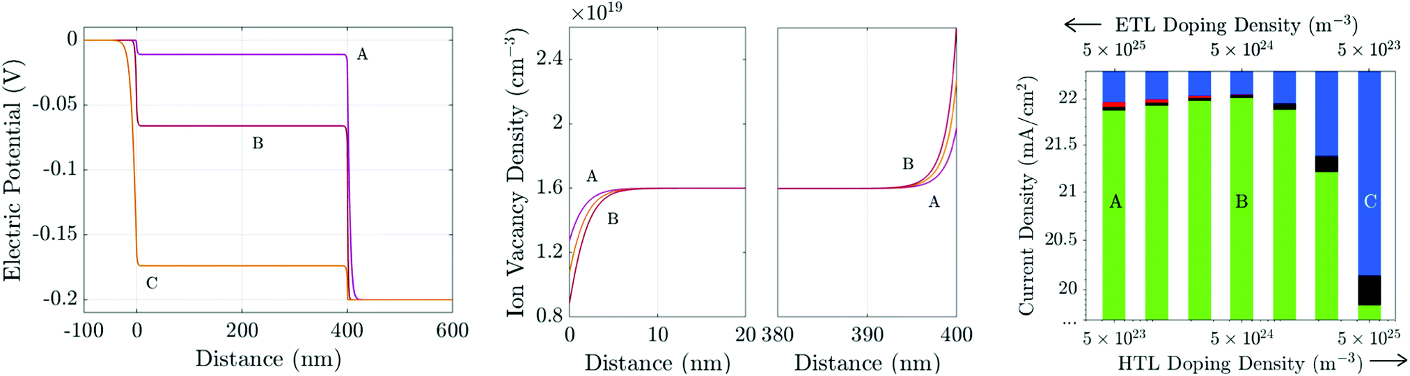 | ||
| Fig. 11 (a) Steady-state potential and (b) ion vacancy profiles for differently-doped TLs held at 0.9 V. The TL doping densities are A: dE = 5 × 1025 m−3, dH = 5 × 10²³ m−3; B: dE = dH = 5 × 1024 m−3; and, C: dE = 5 × 10²³ m−3, dH = 5 × 1025 m−3. All other parameters are as in Tables 1 and 2(b). Panel (c) shows the photocurrent (J, green) and losses due to bulk (R, black) and interfacial (Rr, red; Rl, blue) recombination for a range of TL doping densities including cases A–C above. | ||
Recent experimental work22,23 on PSCs with MAPI absorber layers indicates that in high performing cells interface (rather than bulk) recombination is the performance-limiting mechanism. Here we consider the case where interface recombination, and in particular recombination at the ETL/perovskite interface, dominates by using the recombination parameters in Table 2(b), in which vpE = 10 ms−1 and vnH = 0.1 ms−1.
At steady-state, there is no electric field to separate charge carriers throughout the interior of the perovskite layer. Furthermore, near MPP, the potential drops across the interfacial Debye layers V1 − V4 (as depicted in the inset of Fig. 1) are all positive and so provide energetic barriers to charge injection from the TLs into the perovskite. Thus bulk recombination is largely (although not entirely) unaffected by redistribution of the potential drops between the interfacial Debye layers. It follows that variations in performance between cells with different TL properties arises largely due to differences in interfacial recombination rates. The value of V1 determines the electron concentration in the ETL on the ETL/perovskite interface (i.e. n|x=0− ∝ e−V1/VT) whereas V2 determines the hole concentration in the perovskite on the ETL/perovskite interface (i.e. p|x=0+ ∝ e−V2/VT). Similarly the value of V3 determines the electron concentration in the perovskite on the perovskite/HTL interface (i.e. n|x=b− ∝ e−V3/VT) whereas V4 determines the hole concentration in the HTL on the perovskite/HTL interface (i.e. p|x=b+ ∝ e−V4/VT). Thus for a cell where the dominant loss is due to hole controlled recombination on the ETL/perovskite interface the aim should be to maximise the value of V2 in order to minimise the number of holes reaching the interface from the perovskite. However, since the potential drops V1 − V4 are not independent (see eqn (21) and (22)), the pathway to realising this is not obvious. In contrast if the dominant loss occurs from electron controlled recombination on this interface the aim should be to maximise the value of V1 in order to minimise the number of electrons reaching the interface from the ETL.
In Fig. 11 we investigate the performance of a cell where recombination losses are primarily controlled by recombination occurring on the ETL/perovskite interface and this depends both on the electron concentration in the ETL and on the hole concentration in the perovskite. Moving from left to right in Fig. 11(c) reductions in ETL doping (which increase V1) and increases in HTL doping (which decrease V4) initially result in an improvement in performance, over cell A, by suppressing the electron concentration on the ETL/perovskite interface. However decreasing ETL doping and increasing HTL doping also results in a decrease in V2 and thereby increases the interfacial hole concentration. There is thus an optimal point along this line in changing doping concentration (represented by best performing cell, B) beyond which further decreases in ETL doping and increases in HTL doping result in increased interfacial recombination and poorer performance. This is because after the optimal point the reduction in recombination brought about by further decreases in electron concentration in the ETL are more than offset by the increases in hole concentration in the perovskite.
An important conclusion from this section is that significant potential drops in the perovskite (V2 and V3) are required to improve performance, by keeping holes in the perovskite from recombining on the ETL/perovskite interface and electrons in the perovskite from recombining on the perovskite/HTL interface. Such significant potential drops in the perovskite are associated with the potentially harmful build up of ion vacancies at the edges of the perovskite and also with significant ion migration, and hence hysteresis, during transient measurements. The optimal amount of doping of the TLs must therefore be a balance between creating large energy barriers in the perovskite Debye layers to prevent recombination at the interfaces and screening the potential drop across the perovskite layer to reduce the bulk electric field during transients and hence reduce ion vacancy migration.
5 Conclusions
We demonstrate that ion vacancy migration affects the performance of perovskite solar cells and that the observable effects are strongly dependent on the permittivity and the effective doping density of the transport layers. We find that ion vacancy migration plays a significant role in the steady-state device performance, through the resulting accumulation of ionic charge and band bending in narrow layers adjacent to the interfaces between the perovskite and the transport layers. We show that the distribution of the electric potential is key in determining the transient and steady-state behaviour of a cell. Further to this, we suggest that the doping density and/or permittivities of each transport layer may be tuned to reduce losses due to interfacial recombination. It is not in general possible to give a single recommendation on how these properties should be tuned to improve PCE since the outcome depends strongly on the site at which predominant recombination losses occur. Once this site and the rate limiting charge carrier has been identified our work provides a systematic tool to tune transport layer properties to enhance performance.Our simulations of a three-layer drift-diffusion model reproduce a number of experimental trends, including reduced hysteresis for PSCs with organic transport layers and the ‘reappearance’ of observable hysteresis at low temperature, via adjustment of just a few significant material parameters. Understanding how and which transport layer properties affect cell performance is vital for informing the design of cell architectures. Additionally, we explain how the location of the limiting recombination loss mechanism of experimental devices may be diagnosed from characteristics of a current–voltage curve. Finally we postulate that cells fabricated using transport layers with low permittivity and doping are more stable to degradation, than those made using TLs with high permittivity and doping, since such cells show reduced ion vacancy accumulation within the perovskite Debye layers, which has been linked to chemical degradation at the edges of the perovskite layer.17,18
Conflicts of interest
There are no conflicts to declare.Acknowledgements
NEC and JMC are supported by EPSRC funded studentships from the CDT in New and Sustainable Photovoltaics, reference EP/L01551X/1. ABW is supported by the Energy oriented Centre of Excellence (EoCoE), Horizon2020 grant research number 676629 and by the EPSRC Supersolar Hub Extension EP/P02484X/1. The authors are very grateful to Prof. Laurie Peter for his careful reading of the manuscript and many useful comments.References
- A. Kojima, K. Teshima, Y. Shirai and T. Miyasaka, J. Am. Chem. Soc., 2009, 131, 6050–6051 CrossRef CAS PubMed.
- D.-Y. Son, S.-G. Kim, J.-Y. Seo, S.-H. Lee, H. Shin, D. Lee and N.-G. Park, J. Am. Chem. Soc., 2018, 140, 1358–1364 CrossRef CAS PubMed.
- H. J. Snaith, A. Abate, J. M. Ball, G. E. Eperon, T. C. Leijtens, N. K. Noel, S. D. Stranks, J. T.-W. Wang, K. Wojciechowski and W. Zhang, J. Phys. Chem. Lett., 2014, 5, 1511–1515 CrossRef CAS PubMed.
- G. Richardson, S. E. J. O'Kane, R. G. Niemann, T. A. Peltola, J. M. Foster, P. J. Cameron and A. B. Walker, Energy Environ. Sci., 2016, 9, 1476–1485 RSC.
- Y. Yuan and J. Huang, Acc. Chem. Res., 2016, 49, 286–293 CrossRef CAS PubMed.
- T.-Y. Yang, G. Gregori, N. Pellet, M. Grätzel and J. Maier, Angew. Chem., 2015, 127, 8016–8021 CrossRef.
- A. Senocrate, I. Moudrakovski, G. Y. Kim, T.-Y. Yang, G. Gregori, M. Grätzel and J. Maier, Angew. Chem., Int. Ed., 2017, 56, 7755–7759 CrossRef CAS PubMed.
- C. Eames, J. M. Frost, P. R. F. Barnes, B. C. O'Regan, A. Walsh and M. S. Islam, Nat. Commun., 2015, 6, 7497 CrossRef CAS PubMed.
- W. Nie, H. Tsai, R. Asadpour, J.-C. Blancon, A. J. Neukirch, G. Gupta, J. J. Crochet, M. Chhowalla, S. Tretiak and M. A. Alam, et al. , Science, 2015, 347, 522–525 CrossRef CAS PubMed.
- Y. Shao, Z. Xiao, C. Bi, Y. Yuan and J. Huang, Nat. Commun., 2014, 5, 5784 CrossRef CAS PubMed.
- L. Zheng, D. Zhang, Y. Ma, Z. Lu, Z. Chen, S. Wang, L. Xiao and Q. Gong, Dalton Trans., 2015, 44, 10582–10593 RSC.
- K. Wojciechowski, T. Leijtens, S. Siprova, C. Schlueter, M. T. Hörantner, J. T.-W. Wang, C.-Z. Li, A. K.-Y. Jen, T.-L. Lee and H. J. Snaith, J. Phys. Chem. Lett., 2015, 6, 2399–2405 CrossRef CAS PubMed.
- D. Bryant, S. Wheeler, B. C. O'Regan, T. Watson, P. R. F. Barnes, D. Worsley and J. R. Durrant, J. Phys. Chem. Lett., 2015, 6, 3190–3194 CrossRef CAS.
- N. Courtier, G. Richardson and J. M. Foster, Applied Mathematical Modelling, 2018, 63, 329–348 CrossRef.
- I. Levine, P. K. Nayak, J. T. W. Wang, N. Sakai, S. van Reenen, T. M. Brenner, S. Mukhopadhyay, H. J. Snaith, G. Hodes and D. Cahen, J. Phys. Chem. C, 2016, 120, 16399–16411 CrossRef CAS.
- Z. Li, C. Xiao, Y. Yang, S. P. Harvey, D. H. Kim, J. A. Christians, M. Yang, P. Schulz, S. U. Nanayakkara, C.-S. Jiang, J. M. Luther, J. J. Berry, M. C. Beard, M. M. Al-Jassim and K. Zhu, Energy Environ. Sci., 2017, 10, 1234–1242 RSC.
- N. Aristidou, C. Eames, I. Sanchez-Molina, X. Bu, J. Kosco, M. Islam and S. A. Haque, Nat. Commun., 2017, 8, 15215 CrossRef PubMed.
- W. Nie, J.-C. Blancon, A. Neukirch, K. Appavoo, H. Tsai, M. Chhowalla, M. Alam, M. Sfeir, C. Katan, J. Even, S. Tretiak, J. Crochet, G. Gupta and A. Mohite, Nat. Commun., 2016, 7, 11574 CrossRef CAS PubMed.
- Z. Xiao, Y. Yuan, Y. Shao, Q. Wang, Q. Dong, C. Bi, P. Sharma, A. Gruverman and J. Huang, Nat. Mater., 2014, 14, 193–198 CrossRef PubMed.
- Y. Zhang, M. Liu, G. E. Eperon, T. C. Leijtens, D. McMeekin, M. Saliba, W. Zhang, M. de Bastiani, A. Petrozza, L. M. Herz, M. B. Johnston, H. Lin and H. J. Snaith, Mater. Horiz., 2015, 1, 96 Search PubMed.
- J.-P. Correa-Baena, L. Steier, W. Tress, M. Saliba, S. Neutzner, T. Matsui, F. Giordano, T. J. Jacobsson, A. R. Srimath Kandada, S. M. Zakeeruddin, A. Petrozza, A. Abate, M. K. Nazeeruddin, M. Grätzel and A. Hagfeldt, Energy Environ. Sci., 2015, 8, 2928–2934 RSC.
- C. M. Wolff, F. Zu, A. Paulke, L. P. Toro, N. Koch and D. Neher, Adv. Mater., 2017, 29, 1700159 CrossRef PubMed.
- L. Kegelmann, C. M. Wolff, C. Awino, F. Lang, E. L. Unger, L. Korte, T. Dittrich, D. Neher, B. Rech and S. Albrecht, ACS Appl. Mater. Interfaces, 2017, 9, 17245–17255 CrossRef CAS PubMed.
- H.-S. Kim, I. H. Jang, N. Ahn, M. Choi, A. Guerrero, J. Bisquert and N.-G. Park, J. Phys. Chem. Lett., 2015, 6, 4633–4639 CrossRef CAS PubMed.
- E. Zimmermann, K. K. Wong, M. Müller, H. Hu, P. Ehrenreich, M. Kohlstädt, U. Würfel, S. Mastroianni, G. Mathiazhagan, A. Hinsch, T. P. Gujar, M. Thelakkat, T. Pfadler and L. Schmidt-Mende, APL Mater., 2016, 4, 091901 CrossRef.
- S. van Reenen, M. Kemerink and H. J. Snaith, J. Phys. Chem. Lett., 2015, 6, 3808–3814 CrossRef CAS PubMed.
- W. Tress, N. Marinova, T. Moehl, S. M. Zakeeruddin, M. K. Nazeeruddin and M. Grätzel, Energy Environ. Sci., 2015, 8, 995–1004 RSC.
- N. E. Courtier, J. M. Foster, S. E. J. O'Kane, A. B. Walker and G. Richardson, Eur. J. Appl. Math., 2018 DOI:10.1017/S0956792518000207.
- S. E. J. O'Kane, G. Richardson, A. Pockett, R. G. Niemann, J. M. Cave, N. Sakai, G. E. Eperon, H. J. Snaith, J. M. Foster, P. J. Cameron and A. B. Walker, J. Mater. Chem. C, 2016, 5, 452–462 RSC.
- K. Domanski, B. Roose, T. Matsui, M. Saliba, S.-H. Turren-Cruz, J.-P. Correa-Baena, C. Roldán Carmona, G. Richardson, J. M. Foster, F. De Angelis, J. M. Ball, A. Petrozza, N. Mine, M. K. Nazeeruddin, W. Tress, M. Grätzel, U. Steiner, A. Hagfeldt and A. Abate, Energy Environ. Sci., 2017, 10, 604–613 RSC.
- P. Calado, A. M. Telford, D. Bryant, X. Li, J. Nelson, B. C. O'Regan and P. R. Barnes, Nat. Commun., 2016, 7, 13831 CrossRef CAS PubMed.
- S. Ravishankar, O. Almora, C. Echeverría-Arrondo, E. Ghahremanirad, C. Aranda, A. Guerrero, F. Fabregat-Santiago, A. Zaban, G. Garcia-Belmonte and J. Bisquert, J. Phys. Chem. Lett., 2017, 8, 915–921 CrossRef CAS PubMed.
- D. Jacobs, Y. Wu, H. Shen, C. Barugkin, F. Beck, T. White, K. Weber and K. Catchpole, Phys. Chem. Chem. Phys., 2017, 19, 3094–3103 RSC.
- H. Shen, D. A. Jacobs, Y. Wu, T. Duong, J. Peng, X. Wen, X. Fu, S. K. Karuturi, T. P. White, K. Weber and K. R. Catchpole, J. Phys. Chem. Lett., 2017, 8, 2672–2680 CrossRef CAS PubMed.
- J. Nelson, The Physics of Solar Cells, Imperial College Press, London, UK, 2003 Search PubMed.
- J. Foster, J. Kirkpatrick and G. Richardson, J. Appl. Phys., 2013, 114, 104501 CrossRef.
- P. Löper, M. Stuckelberger, B. Niesen, J. Werner, M. Filipič, S.-J. Moon, J.-H. Yum, M. Topič, S. D. Wolf and C. Ballif, J. Phys. Chem. Lett., 2015, 6, 66–71 CrossRef PubMed.
- J. Emara, T. Schnier, N. Pourdavoud, T. Riedl, K. Meerholz and S. Olthof, Adv. Mater., 2016, 28, 553–559 CrossRef CAS PubMed.
- F. Brivio, K. T. Butler, A. Walsh and M. van Schilfgaarde, Phys. Rev. B: Condens. Matter Mater. Phys., 2014, 89, 155204 CrossRef.
- P. Schulz, E. Edri, S. Kirmayer, G. Hodes, D. Cahen and A. Kahn, Energy Environ. Sci., 2014, 7, 1377 RSC.
- C. C. Stoumpos, C. D. Malliakas and M. G. Kanatzidis, Inorg. Chem., 2013, 52, 9019–9038 CrossRef CAS PubMed.
- A. Walsh, D. O. Scanlon, S. Chen, X. G. Gong and S. H. Wei, Angew. Chem., Int. Ed., 2015, 54, 1791–1794 CrossRef CAS PubMed.
Footnotes |
| † Electronic supplementary information (ESI) available. See DOI: 10.1039/c8ee01576g |
| ‡ As noted in Section 3.6 recombination occurring in the perovskite bulk is very sensitive to the electric field across the perovskite layer which either aids or hinders charge separation depending on its direction. |
| § Note that, as discussed in Section 3.5 the potential is predominantly determined by the ion distribution, and so is for practical purposes independent of the recombination mechanisms. Hence Fig. 7 is equally applicable to the cell dominated by interfacial recombination. |
| This journal is © The Royal Society of Chemistry 2019 |